A differential memristive synapse circuit for on-line learning in neuromorphic computing systems
Abstract
Spike-based learning with memristive devices in neuromorphic computing architectures typically uses learning circuits that require overlapping pulses from pre- and post-synaptic nodes. This imposes severe constraints on the length of the pulses transmitted in the network, and on the network’s throughput. Furthermore, most of these circuits do not decouple the currents flowing through memristive devices from the one stimulating the target neuron. This can be a problem when using devices with high conductance values, because of the resulting large currents. In this paper we propose a novel circuit that decouples the current produced by the memristive device from the one used to stimulate the post-synaptic neuron, by using a novel differential scheme based on the Gilbert normalizer circuit. We show how this circuit is useful for reducing the effect of variability in the memristive devices, and how it is ideally suited for spike-based learning mechanisms that do not require overlapping pre- and post-synaptic pulses. We demonstrate the features of the proposed synapse circuit with SPICE simulations, and validate its learning properties with high-level behavioral network simulations which use a stochastic gradient descent learning rule in two classification tasks.
[datatype=bibtex] \map[overwrite=true] \step[fieldset=url, null] \step[fieldset=doi, null]
-
May 2017
1 Introduction
Neuromorphic computing systems typically comprise neuron and synapse circuits arranged in a massively parallel manner to support the emulation of large-scale spiking neural networks [10, 36, 3, 28, 23, 31, 42, 21]. In these systems, the bulk of the silicon real-estate is taken up by synaptic circuits, where the memory and computational sites are co-localized [23]. Consequently, to save area and maximize density, many neuromorphic computing approaches avoid implementing complex synaptic circuits with on-chip learning mechanisms [28, 32, 41], and resort to training the network on external computers. However, these approaches lose the ability to execute on-line “life-long” learning and require that the network parameters (such as the synaptic weights) be programmed at deployment time. In addition, if these parameters are stored in Static Random Access Memory (SRAM) cells or in Dynamic Random Access Memory (DRAM) banks, they need to be re-programmed every time the system is reset. For large networks [28, 15, 44], the time required to initialize the system with these parameters can become prohibitive.
Memristive devices can potentially address these problems by virtue of their compactness and non-volatility [22]. Given their advantages, several neuromorphic arrays that use memristive devices have been proposed [25, 40, 48, 30, 39]. Typically, these approaches propose to use memristive devices in dense synaptic arrays for implementing large-scale neural networks. For instance, [37, 40] describe use of 1R arrays to implement perceptrons trained by supervised learning protocols such as [45]. Similarly, in [50], the authors train a 1T-1R array to implement perceptrons classifying face images from the Yale face database [17]. In [14], the authors use the Recursive Least-Squares (RLS) algorithm for training synaptic weights to perform complex tasks such as human motor control. In works such as [40, 14], the authors propose the use of two devices per synaptic element to implement positive and negative weight terms. Other approaches describe synaptic arrays with a 1T-1R synapse elements that learn using classical [39, 16, 48, 43, 11] or stochastic [30, 46, 4] Spike-Timing Dependent Plasticity (STDP) learning rules. In these arrays the currents used to program the memristive devices can be very large, especially for devices in high-conductance states. This imposes severe restrictions on the power budget, capacitor sizes, and other aspects for the design of ultra-low power memristive-neuromorphic circuits. Moreover, the learning protocols employed in most of these architectures couple the length of the pulses used to transmit signals across the layers of the network with the duration of the pulses required to program the devices [39, 16]. This requirement imposes severe constraints on the maximum data throughput of the network, because each row or column in the cross-bar array has to wait for the pre- and post-synaptic pulses to finish, before a new one can be sent. In this paper we propose a novel synaptic circuit that addresses at the same time both the large current and overlapping pulses problems. To overcome the problem of integrating large currents in the post-synaptic neuron, we propose a novel differential-mode sub-threshold memristive synapse circuit that decouples, normalizes, and re-scales the memristive device current from the one supplied to the post-synaptic neuron. To overcome the problem of overlapping pulses in cross-bar architectures, we propose an event-based scheme that decouples the duration of the input spikes from the read and update phases of the target synapse, coupled with the use of a novel spike-based synaptic update mechanism.
In recent years, several algorithms employing spike-triggered learning based on post-synaptic neuronal activity, instead of vanilla STDP mechanisms, have been proposed in computational neuroscience literature [6, 20, 49]. Several neuromorphic implementations of these mechanisms have also been realized [31, 19, 42, 21, 33]. In this paper, we demonstrate how the proposed differential memristive synapse circuit can be incorporated in a neuromorphic system that employs a learning circuit based on such ideas. This circuit is inspired by the biologically plausible learning rule presented in [49] and gradient-descent based methods applied to memristive devices [35, 47]. We use these learning circuits to implement a randomized unregulated step descent algorithm, which has been shown to be effective for synaptic elements with limited precision [34].
In the following Section, we present the network architecture that is compatible with the proposed differential memristive synapse circuit. In Section 3 we describe the techniques used for sensing and changing the memristive device conductances, and present circuit simulation results that quantify its performance figures. In Section 4, we assess the features of neuromorphic architectures that make use of the proposed circuits and validate them with behavioral simulations in a binary classification task. Finally, in the Supplementary material we present extensions and variants to the proposed differential synapse memory cell, including their use in dense 1T-1R cross-bar arrays.
2 Neuromorphic architectures for memristive synapses
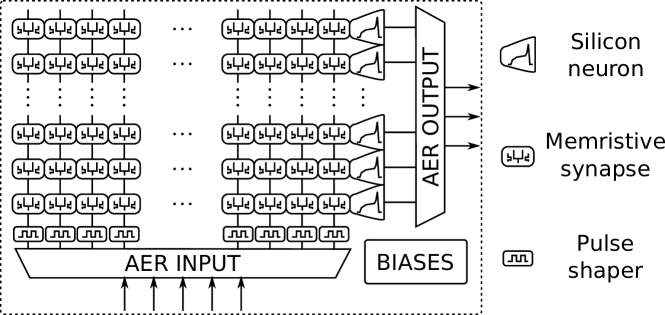
The architecture we propose is composed of an array of synapses and neurons that receive input spikes into columns of synaptic cells, and produce output spikes from the silicon neurons arranged in rows (see Fig. 1). This type of architecture can be integrated within a full-custom neuromorphic Very Large Scale Integration (VLSI) chip, or be used as a single-core in multi-core neuromorphic systems [32, 28]. Both the input and output spikes are represented by fast digital pulses that are encoded using the AER [12, 5, 29, 9].

On the input side, asynchronous AER circuits ensure that events are transmitted as they arrive. Upon the arrival of a pre-synaptic address-event a pulse-shaping circuit decouples the duration of the input spikes from the read and update phases of the target synapse. This frees the communication bus to transmit spikes from sender nodes to the cross-bar array, increasing the throughput of the network by use of shared or time-multiplexed communication resources. The block diagram describing the operation of the pulse-shaping circuits is shown in Fig. 2. The pulse-shaping circuit consists of two pulse-extender circuits [42] and is configured to produce two pulses in quick succession on the arrival of an AER event. These pulses sequentially enable the read-mode operation, where the state of the addressed synapse is sensed, followed by the write-mode operation, where the state of the memristive devices are increased or decreased, in the targetted synapse. The write-mode operation is directed by the UP and DN control signals produced by the learning circuits in the post-synaptic neuron.
On the output side a 1-D arbiter circuit enqueues output events in case of collisions and transmits them on the shared output bus [5]. A programmable bias-generator circuit [13] provides a set of globally-shared temperature-compensated current signals for biasing the analog parameters of the neuromorphic circuits, such as time-constants, refractory periods, or learning rates.
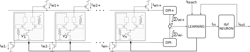
Address-events target destination columns of the memristive array. By construction, all rows of the stimulated column will process the input event in parallel. Furthermore, the extended read and write pulses typically last longer than the input AER event duration. Therefore, a sequential AER stimulation of multiple columns will produce multiple read/write operations across the full array that will overlap in time and operate in parallel. A block diagram of the circuits present in a single row of the cross-bar architecture illustrated in Fig. 1 is shown in Fig. 3. It comprises multiple synaptic circuits that receive the voltage pulses from the pulse-shaping circuits, two current-mode Differential Pair Integrator (DPI) circuits that emulate excitatory and inhibitory synapse dynamics with biologically realistic time constants [1, 2], a current-mode learning block that implements a spike-driven learning mechanism [42, 31], and an ultra-low-power adaptive Integrate-and-Fire (I&F) neuron circuit that faithfully reproduces biologically realistic neural dynamics [27, 24]. In the read-phase, the synaptic circuit senses the state of the two memristive devices in it, and produces rescaled and normalized differential currents that are driven into the positive and negative DPI inputs. The DPI circuits integrate these weighted currents and generate a rescaled output current that is driven into a neuron and its learning block. The learning block uses a copy of this “dendritic” current to compare it to the net input current, which includes contributions from the neuron and an external source. The external source could represent a teacher signal in supervised learning protocols, or contributions from other neurons in unsupervised learning protocols. Based on this comparison, the learning block evaluates an error signal and produces the UP and DN weight update control signals that are used during the write-mode phase to increase or decrease the weights of the stimulated target synapse. We demonstrate the operation of this architecture with a concrete example in Section 4.
3 The differential memristive synapse circuit
The differential memristive synapse circuit is based on the classic Gilbert-normalizer element [18, 26], whose output currents, originally designed for bipolar transistors, but functional also for Metal Oxide Semiconductor Field-Effect Transistors operated in the sub-threshold domain [26]. The synapse circuit stores its weight as the difference between the conductances of two memristive devices, one representing a positive term and the other representing a negative term. Programming the devices is done in a push-pull manner: to increase the synaptic weight, the conductance of the positive term is increased, and that of the negative term is decreased. The complementary operation is achieved by simultaneously decreasing and increasing the conductances of the positive and negative terms, respectively. The output current produced by this circuit, in read-mode, can be scaled to very low values (e.g., in the range of pico Amperes). This reduces the total current driven into the post-synaptic neuron, which can then be implemented with very small capacitors and ultra-low power sub-threshold circuits. The differential operation coupled with the normalizing ability of the circuit has two additional advantages. It reduces the effect of memristive device variability and implements both positive (excitatory) and negative (inhibitory) synapse contributions, effectively doubling the “high-low” dynamic range of the synaptic weight. In write-mode, the circuit enables programming the memristive devices with programmable current limits, pulse widths, and heights. These can be chosen by the user to optimize the write-mode power consumption depending on the memristive device integrated in the circuit.
The operating principles of the circuit is independent of the memristive device technology used. It can be used in combination with a wide range of different resistive memory technologies, with arbitrary number of resistive stable states. In this work we assume our Complementary Metal-Oxide-Semiconductor (CMOS) circuits can be directly interfaced to based devices through post-processing methods, as described in [8].
The schematic diagram of the differential memristive synapse circuit is shown in Fig. 4. The circuit is used in a “read-mode” phase to measure the conductance of the two memristive devices produce scaled output currents that are conveyed to the downstream current-mode neural processing circuits. It is then operated in a “write-mode” for updating the state of the memristive devices via the downstream learning circuit control signals. All MOSFETs represent switches, with gates controlled by digital signals. Signals with an overline, such as , represent the inverted version of the signal . The signal represents the digital voltage used during the read-mode, while the signals and represent the digital set and reset pulses used in the write-mode to increase/decrease the synaptic weight. The signal is a sub-threshold bias voltage that sets the (sub-threshold) scale of the output currents. The MOSFETs have dimensions ; MOSFETs M1 & M4 have , M2 & M3 have , and M5 .
3.1 Read-mode operation
To operate the circuit of Fig. 4 in read-mode, the switches S1, S2, S7, and S8 are turned on and all other switches are turned off; the digital control signals and are set to logical zero. The current-mode normalizer circuit is implemented by MOSFETs M1-M6. In this mode of operation the memristive devices and are connected to corresponding and nodes. When the pulse is active the currents flowing through the memristive devices are measured and the output currents, and , are sent to the excitatory and inhibitory DPI circuits, respectively.

Therefore, in this mode of operation, during a pulse:
| (1) |
where is the current through the device , and is the current through the MOSFET .
For low-power operation, it is desirable to make very small. Under this condition, we can assume that the transistors operate in sub-threshold domain. This allows us to analytically derive the relationship between the circuit parameters, and the current flowing through the circuit’s output branches. By writing the sub-threshold equations for a MOSFET and equating it to the currents through the resistive devices, we get:
| (2) | ||||
where represents the resistance of the memristive device , the supply voltage provided in “read-mode”, the source voltage of the input MOSFETs and , the gate voltage of the MOSFET , the sub-threshold slope factor [26], and the thermal voltage. By solving for :
| (3) |
If is sufficiently small, then
| (4) |
so
| (5) |
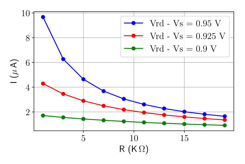
Equation 5 describes how the input current changes with the conductance of the memristive device, and with and voltages. In particular, for large values, the current is approximately linear with respect to the memristive device conductance, but assumes relatively large values (large values make the circuit less power-efficient). For very small voltage differences, the circuit produces very small currents that change linearly, but with a very small dependence on the device memristance . The effect of this trade-off is highlighted in Fig. 5(a), which plots eq. 5 for different values of , with set to 1.8 V. Figure 5(b) shows circuit simulations results, carried out using a standard 130 nm CMOS process, which support the theoretical analysis. was set to 1.8 V, while was swept to obtain the three different values shown in the figure legend. In this mode of operation the voltage applied across the memristive device is set low enough to prevent conductance changes. This allows us to model the device as a fixed resistor, and to characterize the circuit as a function of all resistance values between the memristive device’s low and high resistance states.
The output currents of the differential memristive circuit are directly proportional to the input currents sensed from the corresponding input branch and scaled by the bias current . Specifically,if all transistors operate in sub-threshold saturation domain:
| (6) |
By solving for using the extra condition that , and replacing terms in eq. 3.1, we obtain:
| (7) |
This allows us to produce output currents that are scaled versions of the currents flowing through the memristive devices, and potentially much smaller, thus enabling the design of ultra low-power current-mode memristive sensing architectures. In order to ensure proper operation of the differential memristive output normalizing behavior, while minimizing the power dissipated in the input current sensing stage, it is important to have large values, with small values.
Figure 6 shows the theoretical normalized output current , for a bias current A, for resistance values of increasing from 1K to 20K , and of decreasing proportionally from 20K to 1K . A differential current-mode readout circuit that computes can double the resolution of the conductance/memory state sensing operation.
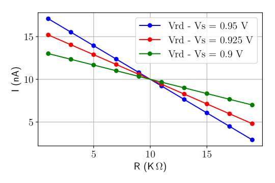
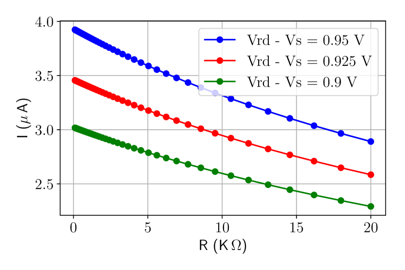
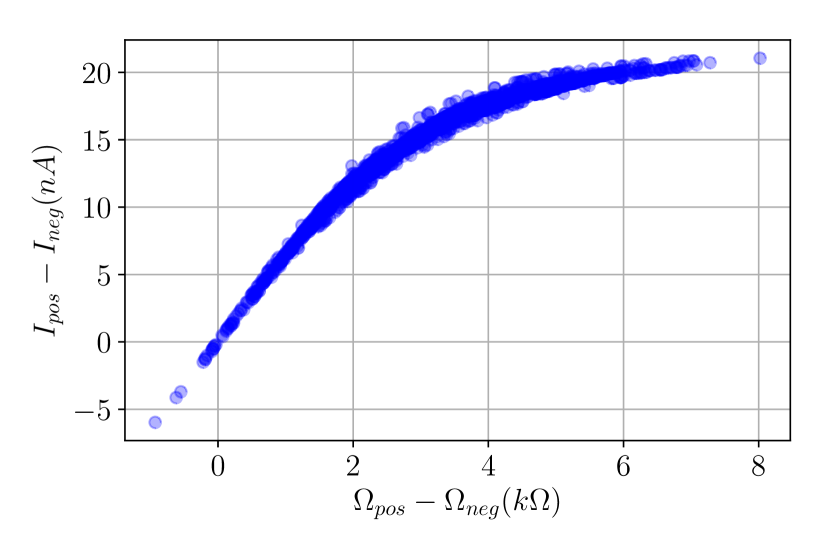
More realistic circuit simulation results for a 130 nm CMOS process are shown in Fig. 7. To generate this plot, the memristive devices were modelled as resistors and the resistance of was swept from to .
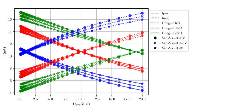
The bias voltage was set to generate a bias current, , of 20 nA. The simulation results show the output of the circuit for different settings of and as a function of different conductance values assumed for the memristive devices. The blue, red, and green traces are the current outputs when the resistance of was set as , , and respectively. The solid and dashed lines plot and respectively. It can be seen from the plots that the cross over point shifts as the resistance values of change. Note how the linearity of the circuit is improved when is reduced, at the cost of slightly reduced difference between and .
3.2 Variability reduction
The strategy to use two memristive devices programmed in a complementary fashion and connected to the current-mode normalizer circuit has the additional benefit of significantly reducing the impact of memristive device variability in the output currents.
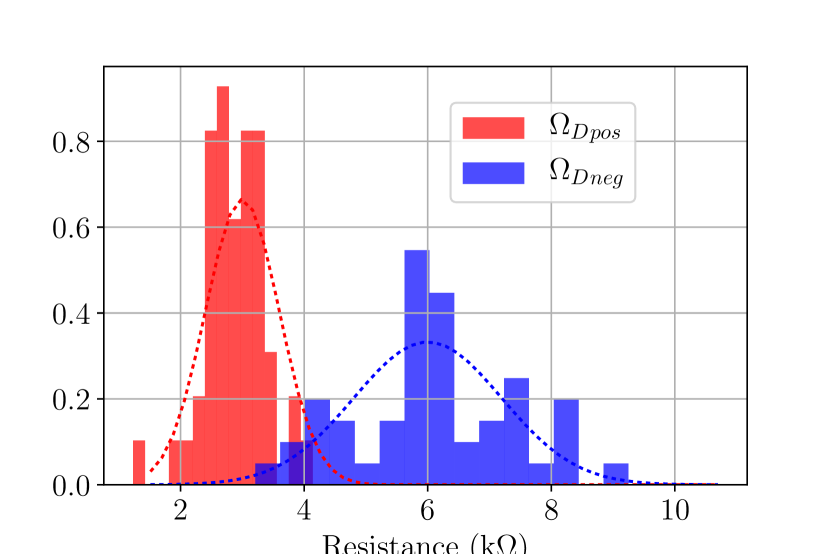
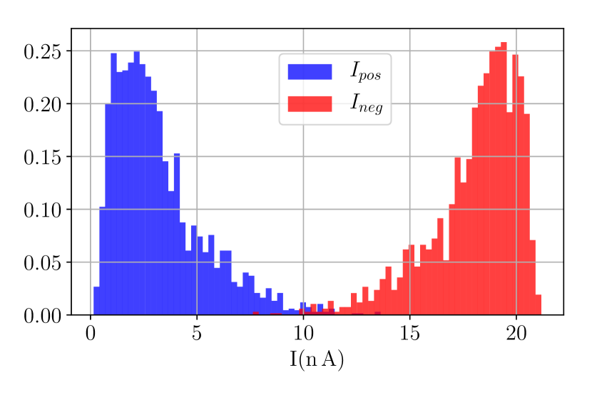
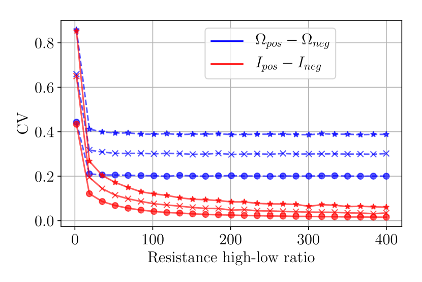
To demonstrate this effect, we show in Fig. 8 the results of Monte Carlo simulations in which we compare the variability of the output currents versus the one of the memristive devices. In these simulations we set and . On the basis of data available from the literature [7], we used conservative figures for the distributions of the memristive device high/low states and their variance. In particular, we sampled resistance values from a Gaussian distribution with (mean,standard deviation) of (6 k,1200 k) and (3 k, 600 ) in the high and low resistance states, respectively (see samples in Fig. 8(a)), and measured the circuit response using such values (see Fig. 8(b)). We observed that the histogram of the output currents and are symmetric, illustrating the effect of normalization, with a standard deviation of approximately for both branches. The normalization circuit effectively compresses the error in output current for large difference between resistances and expands it for small differences as shown in Fig. 8(c). Even for these conservative values of resistance figures, with a very small high-low ratio, the reduction in the Coefficient of Variation (CV) went from 0.429 for the to 0.284 for . For more typical cases, for example with high-low resistance values equivalent to and , the same analysis shows a drastic reduction of CV from 0.219 to 0.003. In Fig. 8 we show a systematic comparison of the CVs between the basic resistance differences and the output current differences, for increasing ratios of high-low states. The comparison was performed running Monte Carlo simulations in which the device high and low resistance states were sampled from a normal distribution with three different coefficients of variation (0.2, 0.3, and 0.4), and the output currents were calculated using the circuit’s transfer function derived analytically in Section 3.
3.3 Write-mode operation
The write-mode operation takes place immediately after the read-mode phase, as determined by the sequence of and pulses generated by the pulse-shaper circuit of Fig. 2. In this phase, is zero, the is high. Furthermore, the switches of two memristive devices (S4-S10) are turned on in a complementary way, such that the resultant voltage across the memristive devices induce opposite changes in their conductance values. For example, to increase the net output current , the conductance of is increased and that of is decreased. This is done by enabling the switches S5, S6, S9, and S10 by programming the signal to logical one, and to logical zero. This connects to , to ground, to , and to ground. Similarly, to decrease , the signal is to set logical one, and is set to logical zero. The MOSFETs M7 and M8 are current-limiting transistors that protect the devices from damage during programming. The signal is a bias voltage chosen that ensure that the memristive devices are not damaged during the forming operation. To minimize power consumption all switching transistors are turned on only during a read or write pulse.
The pulse shaping circuit of Fig 2 can be tuned to increase or decrease the write pulse duration. So by programming the length of these pulses and by choosing appropriate values for and voltages, it is possible to use this circuit to produce reliable binary, gradual, or stochastic changes in the memristive devices [7, 22]. The mode of operation of the memristive devices and the nature of the changes that should be induced in the memristive device conductance depend on the specific learning algorithm implemented in the learning block of Fig. 3.
4 Learning simulations
In this section we demonstrate examples of spike-based learning simulations using a learning rule that is ideally suited for implementation in neuromorphic architectures that comprise the memristive synapse proposed. In the first subsection we learn a single low-dimensional pattern with varying contrast, in the second subsection we learn many overlapping high-dimensional patterns.
4.1 Single pattern binary classification
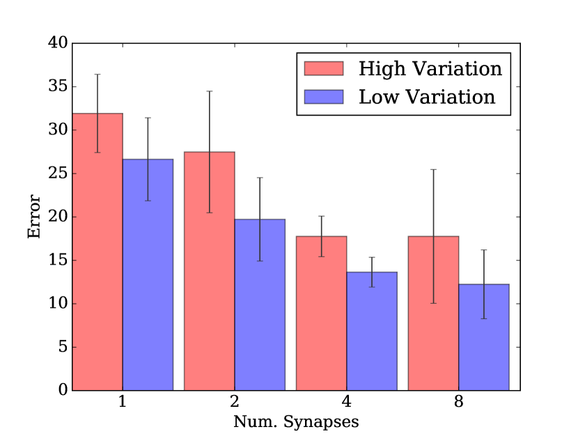
Here we show simulation results of two neurons trained to classify an input spike-train by adjusting their synaptic weights. We study the performance of such a learning system connected by multiple binary synapses and compare it to that of a hypothetical 32-bit floating-point precision synapse in the same setting. This illustrates what the performance limitation is with an ‘ideal’ synaptic element for classifying a finite-rate Poisson train with a leaky integrator neuron.
In this task, the neurons and are connected via randomly initialized synapses to two neural populations and , which fire with two different average firing rates, with Poissonian statistics. The goal is for neuron to learn to fire more than neuron , whenever input units from population fire at a higher rate than input units in . To achieve this, we use a supervised training protocol: given the input, we provide a teacher signal to the neuron that should fire more. The teacher signal is represented by a Poissonian spike train sent to the target neurons via an additional, separate, channel. The spike-based learning algorithm is a discretized version of the one presented in [49]. It performs a gradient descent procedure on the difference of the observed and desired neuron firing rates, and it can be readily implemented in mixed signal CMOS neuromorphic hardware [34, 42]. A detailed description of this learning rule and the parameter values used are provided in the Supplementary Material.

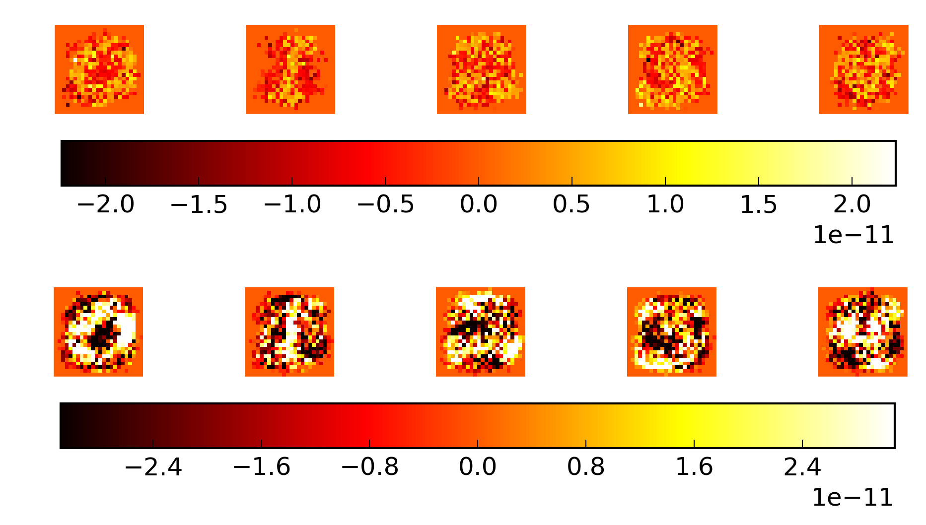
In Fig. 9 we compare the classifications results produced by the best system using a 32-bit floating-point precision synapse with the results obtained simulating the proposed binary synapse in the same setting. Each of the two variables is proportional to the firing rate of the respective subpopulation. When they are equal the pattern has no ‘constrast’, when they are very different it is strongly contrasted. The colors indicate which of the two learning neurons fired more strongly; the ideal solution is a separation of red and blue at a angle. The proposed learning rule finds a good solution to the classification problem, in that the misclassified points only elicit a slightly higher response in the wrong output neuron.
4.2 Classifying multiple patterns
Here we show how it is possible to train a population of output neurons to classify multiple overlapping patterns in a supervised setting. For this demonstration we use the common benchmark of classifying handwritten digits from the MNIST data-set. Namely we test the system using MNIST digits from 0 to 4 scaled to pixels, as in [4]. In the network, there is an input layer consisting of Poisson neurons, whose spike rates are scaled according to the intensity of the MNIST digit image pixel, and the output layer consisting of 5 neurons that should learn to respond to the corresponding digit, and an additional layer of teacher neurons indicating which of 5 output neurons should fire in response to a given input. The index of the output neuron that fires the most in response to a test stimulus is considered the label that the network assigns to this input. During training 1000 digits, randomly drawn from the training set, are presented for ms each while the learning circuits are enabled. The learning circuits are then disabled and the performance of the network is evaluated on 500 further digits (randomly drawn from the test set). Further implementation details are given in the supplementary material.
The learning algorithm is the same one used in Section 4.1. To compensate for the discretization errors, the update is made probabilistic as in [34]. Although we restrict ourselves to probabilistic signals that are independent per neuron, rather than per synapse, we achieve a performance comparable to that of [4].
5 Discussion
The memristive synapse circuit proposed in this paper comprises two memristive devices, 20 MOSFETss, and a pulse controller module. Clearly, the resulting synaptic circuit is much larger in area than synapse elements employed in dense 1R or 1T-1R crossbar arrays [16, 38, 40]. However, the large area overhead used allows the system to operate multiple synapses in parallel, both along the rows and along the columns of the synaptic array (e.g., by sending multiple AER pulses in quick succession across multiple columns). In addition, as the currents passing through the memristive devices are contained in each individual synapse element and do not diffuse to neighboring devices, there are no sneak-path issues and no problems for quickly charging/discharging high capacitive loads. The strategy of using two memristive devices per synapse allows the use of a normalizer circuit, which has the desirable property of minimizing the effect of variability across the memristive devices. In addition, the strategy adopted to use the two devices in a differential way, increasing one while decreasing the other, eliminates the need for a precise reference for the normalizer operations, and provides automatically the possibility to implement both positive and negative synaptic weights in the network.
6 Conclusion
We proposed a differential current-mode memristive synapse circuit that decouples the current used to sense or change memristive device state from the current used to stimulate ultra low-power post-synaptic neuron circuits. We showed that the circuit proposed significantly reduces the effect of device variability, and that it is ideally suited for implementing advanced spike-based learning mechanisms that do not use overlapping pulses at the terminals of the target synapse. We argued that the strategy of using pulse extenders and Gilbert-normalizers in each synapse element maximizes throughput and minimizes power consumption in large-scale event-based neuromorphic computing platforms. For applications that do no require online adpatation or simultaneous read-write functionality, we describe how the synaptic circuit can be integrated with dense memristive crossbar arrays (Supplementary material). Given that memory-related constraints, such as size and throughput, represent one of the major bottlenecks in conventional computing architectures [23], and given the potential of neuromorphic computing platforms to perform robust computation using variable and slow computing elements, the proposed circuit offers an attractive solution for building alternative non von Neumann computing platforms with advanced and emerging memory technologies.
7 Acknowledgements
This work was supported by SNSF grant number CRSII2_160756 and by the EU ICT grant “NeuRAM3” (687299).
References
- [1] C. Bartolozzi and G. Indiveri “Synaptic dynamics in analog VLSI” In Neural Computation 19.10, 2007, pp. 2581–2603
- [2] C. Bartolozzi, S. Mitra and G. Indiveri “An ultra low power current–mode filter for neuromorphic systems and biomedical signal processing” In Biomedical Circuits and Systems Conference, (BioCAS), 2006, 2006, pp. 130–133 IEEE
- [3] Ben Varkey Benjamin et al. “Neurogrid: A Mixed-Analog-Digital Multichip System for Large-Scale Neural Simulations” In Proceedings of the IEEE 102.5 IEEE, 2014, pp. 699–716
- [4] J. Bill and R. Legenstein “A compound memristive synapse model for statistical learning through STDP in spiking neural networks” In Frontiers in neuroscience 8 Frontiers Media SA, 2014
- [5] K.A. Boahen “Point-to-Point Connectivity Between Neuromorphic Chips Using Address-Events” In IEEE Transactions on Circuits and Systems II 47.5, 2000, pp. 416–34
- [6] J. Brader, W. Senn and S. Fusi “Learning real world stimuli in a neural network with spike-driven synaptic dynamics” In Neural Computation 19, 2007, pp. 2881–2912
- [7] S Brivio et al. “Experimental study of gradual/abrupt dynamics of HfO2-based memristive devices” In Applied Physics Letters 109.13 AIP Publishing, 2016, pp. 133504
- [8] Hong-Yu Chen et al. “Resistive random access memory (RRAM) technology: From material, device, selector, 3D integration to bottom-up fabrication” In Journal of Electroceramics, 2017
- [9] E. Chicca et al. “A multi-chip pulse-based neuromorphic infrastructure and its application to a model of orientation selectivity” In IEEE Transactions on Circuits and Systems I 5.54, 2007, pp. 981–993
- [10] E. Chicca, F. Stefanini, C. Bartolozzi and G. Indiveri “Neuromorphic electronic circuits for building autonomous cognitive systems” In Proceedings of the IEEE 102.9, 2014, pp. 1367–1388
- [11] Erika Covi et al. “Analog memristive synapse in spiking networks implementing unsupervised learning” In Frontiers in neuroscience 10 Frontiers Media SA, 2016
- [12] S.R. Deiss, R.J. Douglas and A.M. Whatley “A Pulse-Coded Communications Infrastructure for Neuromorphic Systems” In Pulsed Neural Networks MIT Press, 1998, pp. 157–78
- [13] T. Delbruck, R. Berner, P. Lichtsteiner and C. Dualibe “32-bit Configurable bias current generator with sub-off-current capability” In International Symposium on Circuits and Systems, (ISCAS), 2010 Paris, France: IEEE, 2010, pp. 1647–1650 IEEE
- [14] Lei Deng et al. “Complex Learning in Bio-plausible Memristive Networks” In Scientific reports 5 Nature Publishing Group, 2015
- [15] S.B. Furber, F. Galluppi, S. Temple and L.A. Plana “The SpiNNaker Project” In Proceedings of the IEEE 102.5, 2014, pp. 652–665
- [16] Daniele Garbin et al. “HfO 2-based OxRAM devices as synapses for convolutional neural networks” In IEEE Transactions on Electron Devices 62.8 IEEE, 2015, pp. 2494–2501
- [17] A Georghiades, PN Belhumeur and DJ Kriegman “Yale face database” In Center for computational Vision and Control at Yale University, http://cvc. yale. edu/projects/yalefaces/yalefa 2, 1997
- [18] B. Gilbert “Current-Mode Circuits from a Translinear Viewpoint: A Tutorial” In Analogue IC design: the current-mode approach Stevenage, Herts., UK: Peregrinus, 1990, pp. 11–91
- [19] M. Giulioni et al. “Robust working memory in an asynchronously spiking neural network realized in neuromorphic VLSI” In Frontiers in Neuroscience 5.149, 2012
- [20] M. Graupner and N. Brunel “Calcium-based plasticity model explains sensitivity of synaptic changes to spike pattern, rate, and dendritic location” In Proceedings of the National Academy of Sciences 109, 2012, pp. 3991–3996
- [21] Frank L Maldonado Huayaney, Stephen Nease and Elisabetta Chicca “Learning in Silicon Beyond STDP: A Neuromorphic Implementation of Multi-Factor Synaptic Plasticity With Calcium-Based Dynamics” In IEEE Transactions on Circuits and Systems I: Regular Papers 63.12 IEEE, 2016, pp. 2189–2199
- [22] Daniele Ielmini and Rainer Waser “Resistive Switching: From Fundamentals of Nanoionic Redox Processes to Memristive Device Applications” John Wiley & Sons, 2015
- [23] G. Indiveri and S.-C. Liu “Memory and information processing in neuromorphic systems” In Proceedings of the IEEE 103.8 IEEE, 2015, pp. 1379–1397
- [24] G. Indiveri et al. “Neuromorphic silicon neuron circuits” In Frontiers in Neuroscience 5, 2011, pp. 1–23
- [25] Sung Hyun Jo et al. “Nanoscale memristor device as synapse in neuromorphic systems” In Nano letters 10.4 ACS Publications, 2010, pp. 1297–1301
- [26] S.-C. Liu et al. “Analog VLSI:Circuits and Principles” MIT Press, 2002
- [27] P. Livi and G. Indiveri “A current-mode conductance-based silicon neuron for Address-Event neuromorphic systems” In International Symposium on Circuits and Systems, (ISCAS), 2009, 2009, pp. 2898–2901 IEEE
- [28] Paul A. Merolla et al. “A million spiking-neuron integrated circuit with a scalable communication network and interface” In Science 345.6197, 2014, pp. 668–673
- [29] P.A. Merolla, J.V. Arthur, B.E. Shi and K.A. Boahen “Expandable Networks for Neuromorphic Chips” In IEEE Transactions on Circuits and Systems I 54.2, 2007, pp. 301–311
- [30] V Milo et al. “Demonstration of hybrid CMOS/RRAM neural networks with spike time/rate-dependent plasticity” In Electron Devices Meeting (IEDM), 2016 IEEE International, 2016, pp. 16–8 IEEE
- [31] S. Mitra, S. Fusi and G. Indiveri “Real-time classification of complex patterns using spike-based learning in neuromorphic VLSI” In Biomedical Circuits and Systems, IEEE Transactions on 3.1 IEEE, 2009, pp. 32–42
- [32] S. Moradi, G. Indiveri, N. Qiao and F. Stefanini “Networks and hierarchical routing fabrics with heterogeneous memory structures for scalable event-driven computing systems” Filed 27.04.2015, European patent application EP 15/165272, 2015
- [33] Hesham Mostafa, Christian Mayr and Giacomo Indiveri “Beyond spike-timing dependent plasticity in memristor crossbar arrays” In Circuits and Systems (ISCAS), 2016 IEEE International Symposium on, 2016, pp. 926–929 IEEE
- [34] L. Müller, M. Nair and G. Indiveri “Randomized Unregulated Step Descent for Limited Precision Synaptic Elements” submitted In International Symposium on Circuits and Systems, (ISCAS), 2017, 2017 IEEE
- [35] Manu V Nair and Piotr Dudek “Gradient-descent-based learning in memristive crossbar arrays” In Neural Networks (IJCNN), 2015 International Joint Conference on, 2015, pp. 1–7 IEEE
- [36] Jongkil Park et al. “A 65k-neuron 73-Mevents/s 22-pJ/event asynchronous micro-pipelined integrate-and-fire array transceiver” In Biomedical Circuits and Systems Conference (BioCAS), 2014 IEEE, 2014, pp. 675–678 IEEE
- [37] Sangsu Park et al. “Electronic system with memristive synapses for pattern recognition” In Scientific reports 5 Nature Publishing Group, 2015, pp. 10123
- [38] S Park et al. “RRAM-based synapse for neuromorphic system with pattern recognition function” In Electron Devices Meeting (IEDM), 2012 IEEE International, 2012, pp. 10–2 IEEE
- [39] G Pedretti et al. “Memristive neural network for on-line learning and tracking with brain-inspired spike timing dependent plasticity” In Scientific Reports 7 Nature Publishing Group, 2017
- [40] Mirko Prezioso et al. “Training and operation of an integrated neuromorphic network based on metal-oxide memristors” In Nature 521.7550 Nature Research, 2015, pp. 61–64
- [41] N. Qiao and G. Indiveri “Scaling mixed-signal neuromorphic processors to 28nm FD-SOI technologies” In Biomedical Circuits and Systems Conference, (BioCAS), 2016, 2016, pp. 552–555 IEEE
- [42] Ning Qiao et al. “A Re-configurable On-line Learning Spiking Neuromorphic Processor comprising 256 neurons and 128K synapses” In Frontiers in Neuroscience 9.141, 2015
- [43] S. Saighi et al. “Plasticity in memristive devices” In Frontiers in Neuroscience 9.51, 2015
- [44] J. Schemmel et al. “A wafer-scale neuromorphic hardware system for large-scale neural modeling” In Circuits and Systems (ISCAS), Proceedings of 2010 IEEE International Symposium on, 2010, pp. 1947–1950 IEEE
- [45] W Schiffmann, M Joost and R Werner “Optimization of the backpropagation algorithm for training multilayer perceptrons” In University of Koblenz: Institute of Physics, 1994
- [46] Alexander Serb et al. “Unsupervised learning in probabilistic neural networks with multi-state metal-oxide memristive synapses” In Nature communications 7 Nature Publishing Group, 2016, pp. 12611
- [47] Daniel Soudry et al. “Memristor-based multilayer neural networks with online gradient descent training” In IEEE transactions on neural networks and learning systems 26.10 IEEE, 2015, pp. 2408–2421
- [48] Manan Suri et al. “Phase change memory as synapse for ultra-dense neuromorphic systems: Application to complex visual pattern extraction” In Electron Devices Meeting (IEDM), 2011 IEEE International, 2011, pp. 4–4 IEEE
- [49] Robert Urbanczik and Walter Senn “Learning by the dendritic prediction of somatic spiking” In Neuron 81.3 Cell Press, 2014, pp. 521–528
- [50] Peng Yao et al. “Face classification using electronic synapses” In Nature Communications 8 Nature Publishing Group, 2017