Shiba Bound States across the mobility edge in doped InAs nanowires
Abstract
We present a study of Andreev Quantum Dots (QDots) fabricated with small-diameter (30 nm) Si-doped InAs nanowires where the Fermi level can be tuned across a mobility edge separating localized states from delocalized states. The transition to the insulating phase is identified by a drop in the amplitude and width of the excited levels and is found to have remarkable consequences on the spectrum of superconducting SubGap Resonances (SGRs). While at deeply localized levels, only quasiparticles co-tunneling is observed, for slightly delocalized levels, Shiba bound states form and a parity changing quantum phase transition is identified by a crossing of the bound states at zero energy. Finally, in the metallic regime, single Andreev resonances are observed.
pacs:
Valid PACS appear hereIn superconductor-QDot-superconductor structures or at impurities in bulk superconductors, Bogoliubov type bound states can form at energy smaller than the superconducting gap energy , leading to SGRs.
The SGR formation depends on the different energy scales: , the coupling of the QDot with the superconducting electrodes, the charging energy, U, and the energy, , of the QDot level relative to the Fermi energy of the superconducting electrodes. Its phase diagram has been extensively studied theoreticallyRozhkov and Arovas (1999); Martín-Rodero and Yeyati (2011). For large coupling , the SGRs result from the coherent superposition of multiple Andreev reflectionsKulik (1969); Octavio et al. (1983) and conductance peaks are expected at voltage values /neScheer et al. (1998) where n is the number of Andreev reflections. For weak coupling , where the system is in the regime of Coulomb blockade, the ground state, singlet or doublet , results from the competition between the Kondo screening and the superconducting pairing interaction. These two ground states are separated by a parity changing quantum phase transition, which can be identified by the crossing of the SGRs at zero-energy. Previous works have addressed this transition through measurements of Josephson supercurrentsvan Dam et al. (2006); Cleuziou et al. (2006); Jørgensen et al. (2007); Maurand et al. (2012); Kanai et al. (2010) and studies of the SGRs in S-QDot-S Eichler et al. (2007); Sand-Jespersen et al. (2007); Pillet et al. (2010); Deacon et al. (2010a); Giazotto et al. (2011); Pillet et al. (2013); Kumar et al. (2014) or N-QDot-S geometriesDirks et al. (2010); Deacon et al. (2010b); Lee et al. (2012); Chang et al. (2013). Recently, similar devices attracted intense interest with the observation of the zero-energy Majorana end states in proximitized nanowiresMourik et al. (2012); Das et al. (2012); Deng et al. (2012).
The physics of odd parity QDot is related to the physics of Shiba statesYu (1965); Shiba (1968); Rusinov (1969); Soda et al. (1967); Shiba and Soda (1969) forming at magnetic impurities in bulk superconductors, where tuning the magnetic exchange also leads to a parity changing quantum phase transitionSakurai (1970); Satori et al. (1992); Simonin and Allub (1995); Salkola et al. (1997); Balatsky et al. (2006); Bauer et al. (2007); Tsai et al. (2009), characterized by a crossing of the Shiba states at zero energyFranke et al. (2011).
So far, the impurity induced superconducting SGRs have been only observed by Scanning Tunneling Microscopy, at Co atoms deposited on NbYazdani et al. (1999), at magnetic impurities in 2H-NbSe2Ménard et al. (2015) and magnetic MnPc molecules deposited on PbFranke et al. (2011). However, tunneling spectroscopy of impurity states can also be done with microfabricated devices, such as nano-sized Schottky diodes Calvet et al. (2002), nanosized field effect transistors Sellier et al. (2006); Calvet et al. (2011, 2007a, 2007b) or nanosized memristorsMottaghizadeh et al. (2014). In this work, we present an observation of Shiba bound states forming in a dopant-induced impurity band. In this diffusive regime, it is expected that an Anderson-like Metal-Insulator Transition (MIT)Lee (1985) separates the metallic regime at high carrier concentration from an insulating regime at low carrier concentration, where the localized and delocalized states in the band structure are separated in energy by a mobility edge. We identified this mobility edge in the conductance spectrum measured as function of gate voltage and show that the SGRs are sensitive to the metal-insulator transition through the effect of localization on the coupling parameter .
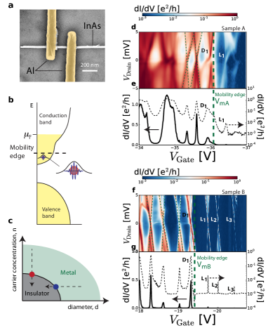
Epitaxially grown InAs nanowires of diameter approximately d=30 nmGlas et al. (2007) were deposited on a degenerately doped Si substrate covered with a 300 nm thick thermal oxide. The nanowires are contacted with e-beam deposited Ti(5 nm)/Al (100 nm) electrodes with moderate in-situ ion beam cleaning of the nanowire surface before deposition. Fig. 1a shows an SEM image of one device. About 20 devices have been fabricated and measured with a standard lock-in method. The room temperature resistivity is below 10 m.cm, which is 20 times smaller than the value measured for undoped nanowires of similar diameterScheffler et al. (2009). The two-wires and four-wires resistance are similar, indicating negligible contact resistance. Two devices, sample A and sample B, have been extensively measured in a dilution fridge with a base temperature of 30 mK. Upon cooling, the resistivity increases only up to 15 m.cm, which is 2 smaller than measured on undoped nanowires, indicating metallic behavior as shown now.
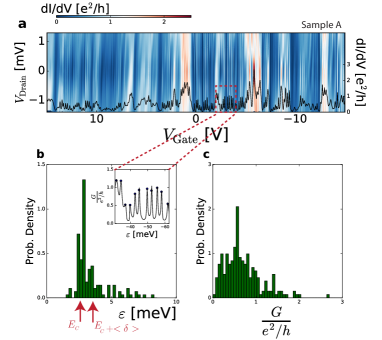
Fig. 1d and Fig. 1f show conductance maps dI/dV as function of drain and gate bias for sample A and sample B, respectively. They are measured with a large AC voltage (V) on a large drain voltage range, making the superconducting-like features barely visible. They show Coulomb blockade diamonds from which the lever arms and the corresponding capacitances are obtainedIhn (2004). The Coulomb energy extracted from the gate voltage separation between nodes is given by =emeV for sample A, EC=4.4 meV for sample B.
Upon depleting the nanowire with a negative back-gate voltage, one can identify a threshold, =-36 V, =-19.4 V, for nanowires A and B, Fig. 1e and Fig. 1g, respectively, below which the excitation lines, labelled L1 to L3, are much narrower and their amplitude much weaker than the excitation lines above the threshold. For nanowire B, the amplitude of the Coulomb peak maxima ==0.12, =0.01, normalized to the amplitude of the last level D1 above the threshold, decreases with the energy of the levels, indicating that the lower energy levels are more strongly localized. This striking evolution across the threshold indicates that it corresponds to the mobility edge where the states of energy above the mobility edge are delocalized and the states below are localized due to Anderson localization. For both samples, no other excitation levels are observed at gate voltages lower than the localized levels, indicating that the nanowires are indeed completely depleted at these most negative voltages, as shown on the zero bias conductance measured on a large gate voltage range shown Fig. S1. In past works on phosphorus doped nanosized metal-Si-metal structuresSellier et al. (2006), dopant levels have also been identified as sharp conductance lines below the pinch-off voltage where the channel is fully depleted.
From these voltage thresholds, an estimation of the carrier concentration at near-zero gate bias is obtained from the relation n=CGVmA(B)/(el), where l is the distance between the electrodes. Ones find cm-3 for sample A (l=100 nm) and cm-3 for sample B (l=200 nm). This carrier concentration is 10 times larger than in undoped nanowiresScheffler et al. (2009). Assuming that each Si atom provides one electron, each QDot contains dopants per 100 nm unit length. For this density, the average distance between dopants is nm, which is smaller than the Bohr radius nm, calculated from the relation with and the effective mass . In other words, the carrier concentration is much larger than critical density cm-3 obtained from the Mott criterionMott (1990) 0.25 for metallicity. At this high doping level, an impurity band is expected to form and merge with the conduction band, as sketched Fig. 1b, Ref. Schubert (2015). As discussed by MottMott (1990), the Ioffe-Regel criterion for metallicity implies that a mobility edge separates the delocalized states () at high energy from the Anderson localized states () at low energy. Thus, a MIT is expected either as function of disorder or carrier concentration as sketched on the phase diagram Fig. 1c. In nanowires, the amount of disorder is controlled by the diameter, as shown in Ref. Scheffler et al. (2009) where the mobility of undoped nanowires drops abruptly below a critical diameter about 50 nm, which corresponds to a disorder driven MIT. In contrast, while our nanowires have a diameter smaller than this critical diameter, they are metallic because of their high carrier concentration. They are driven into the insulating regime upon reducing the carrier concentration with the gate voltage.
An indication that the excitation levels observed above the mobility edge are also part of the impurity band comes from the level spacings, which is expected to show large fluctuations as a consequence of the random dopant distribution. The conductance map Fig. 2a for sample A reveals more than 140 Coulomb diamonds measured at low gate bias above the mobility edge. The corresponding histogram of level spacings is shown Fig. 2b. Because the precision on the determination of the level spacing d meV is smaller than the width 4.2 meV of the histogram, this broad histogram clearly indicates fluctuating level spacing in the nanowire. In this metallic regime, the level spacing distribution is described by random matrix theoryAlhassid (2000); Beenakker (1997), which predicts a bimodal Wigner distribution. This distribution is characterized by two maxima. One is at the Coulomb energy , the other at , where = 1 meV is the mean level spacing calculated from the relation where is the density of states, meV is the Fermi energy corresponding to the estimated carrier density and is the volume of the QDot. The position of these two peaks are indicated on the histogram Fig. 2b.
In the random matrix theory, the random distribution of level spacings is accompanied by a random distribution of the amplitude of the wavefunctions at the boundaries of the QDot, which leads to a broad distribution of the conductance of the Coulomb peak maxima, as observed experimentally and shown in Fig. 2c. This last observation implies strong fluctuations in the coupling of the levels to the superconducting electrodes which has important consequence on the formation of the superconducting SGRs. Finally, from the magnetic field dependence of the Zeeman splitting, Fig. S3, a factor g is extracted, which is consistent with known values of the g-factor in InAsCsonka et al. (2008).
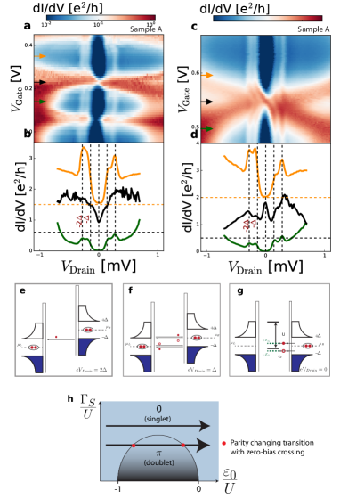
Figure 3a,b show conductance maps measured at low bias. It reveals the superconducting gap of Al with 4 lines symmetric about zero bias. Inside the Coulomb diamonds, the horizontal conductance ridges at eVDrain = 2 correspond to the onset of elastic quasiparticle co-tunneling where the peaks in the density of states of the two superconducting electrodes are aligned, as sketched Fig. 3e. The superconducting gap value V is extracted, which is similar to values obtained in past worksBuizert et al. (2007). This figure also shows conductance ridges at eV. They correspond to n=1 Andreev reflections as depicted Fig. 3h. They are generally expected in SNS structuresOctavio et al. (1983); Martín-Rodero and Yeyati (2011), where the coupling to the electrodes is large, which corresponds to the singlet ’0’ regime in the phase diagram, Fig.3h. They have been observed previously in InAs nanowiresSand-Jespersen et al. (2007) and carbon nanotubesBuitelaar et al. (2003); Eichler et al. (2007); Grove-Rasmussen et al. (2009); Pillet et al. (2010). For certain gate voltages, the pair of Andreev conductance peaks crosses at zero-bias, as shown Fig. 3c and Fig.S2. This zero-bias crossing is the consequence of a quantum phase transition with parity change of the S-QDot-S ground stateMartín-Rodero and Yeyati (2011) from the singlet ’0’ state to the doublet ’’ state. This transition is expected at low coupling as indicated on the phase diagram Fig. 3h. The origin of these occasional zero-bias crossing is the consequence of fluctuating coupling to the electrodes as discussed above. Only those levels which are weakly coupled will show a zero-bias crossing. All these superconducting-like features disappear by the application of a small magnetic field about 20 mT.
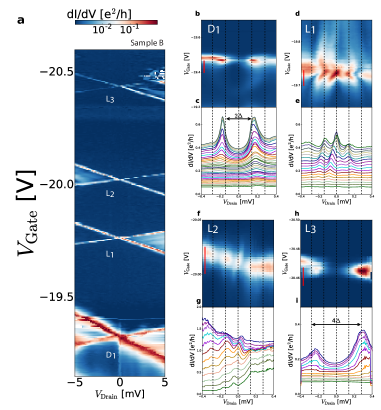
We now turn to the evolution of the SGRs across the mobility edge. As a consequence of the decreasing coupling of the levels with the superconducting electrodes, the high resolution zoom, Fig. 4, shows a remarkable evolution of the SGRs spectrum from the last delocalized level D1 to the localized levels L1 to L3. The level D1 shows mostly conductance ridges at . This is the singlet ’0’ regime dominated by the n=1 Andreev reflections that occur at strong coupling. The first and second localized levels, L1 and L2, show a crossing of the SGRs at zero-energy. This crossing indicates a parity change and the formation of a Shiba resonance at the Si impurity carrying a single electron spin; this is the doublet ’’ regime that occurs at weak coupling in the phase diagram Fig. 3g. Finally, the last level L3 shows only the superconducting gap features at 2, which are the signatures of quasiparticle co-tunneling. This last level is so localized and weakly coupled to the electrodes that no Andreev reflection occurs in the QDot.
To summarize, while past works on InAs based Andreev QDots employed large diameter nanowires ( nm), we found that Andreev QDots could be fabricated with smaller (30 nm) diameter nanowires provided that they are initially doped to high carrier concentration of cm-3. We found that these nanowires could be driven across an Anderson MIT upon applying a large negative back gate voltage and we observed a remarkable evolution of the superconducting SGRs across the mobility edge as consequence of the rapidly changing coupling of the levels with the superconducting electrodes. Deeply localized levels do not allow for the presence of Andreev reflections or the formation of Shiba states and only quasiparticles co-tunneling is observed. For localized levels near the mobility edge, Shiba bound states form and a parity changing quantum phase transition is identified by a crossing of the SGRs at zero energy. Finally, just above the mobility edge, simple n=1 Andreev resonances are observed. Further studies of SGRs in disordered QDots could provide insight into the Anderson MIT, which remains a subject of intense theoretical interestBelitz and Kirkpatrick (1994); Evers and Mirlin (2008).
References
- Rozhkov and Arovas (1999) A. V. Rozhkov and D. P. Arovas, Phys. Rev. Lett. 82, 2788 (1999).
- Martín-Rodero and Yeyati (2011) A. Martín-Rodero and A. L. Yeyati, Adv. Phys. 60, 899 (2011).
- Kulik (1969) I. O. Kulik, Soviet Journal of Experimental and Theoretical Physics 30, 944 (1969).
- Octavio et al. (1983) M. Octavio, M. Tinkham, G. E. Blonder, and T. M. Klapwijk, Phys. Rev. B: Condens. Matter Mater. Phys. 27, 6739 (1983).
- Scheer et al. (1998) E. Scheer, N. Agraït, J. C. Cuevas, A. L. Yeyati, B. Ludoph, A. Martín-Rodero, G. R. Bollinger, J. M. van Ruitenbeek, and C. Urbina, Nature 394, 154 (1998).
- van Dam et al. (2006) J. a. van Dam, Y. V. Nazarov, E. P. a. M. Bakkers, S. De Franceschi, and L. P. Kouwenhoven, Nature 442, 667 (2006).
- Cleuziou et al. (2006) J.-P. Cleuziou, W. Wernsdorfer, V. Bouchiat, T. Ondarçuhu, and M. Monthioux, Nat. Nanotechnol. 1, 53 (2006).
- Jørgensen et al. (2007) H. I. Jørgensen, T. Novotný, K. Grove-Rasmussen, K. Flensberg, and P. E. Lindelof, Nano Lett. 7, 2441 (2007).
- Maurand et al. (2012) R. Maurand, T. Meng, E. Bonet, S. Florens, L. Marty, and W. Wernsdorfer, Physical Review X 2, 011009 (2012).
- Kanai et al. (2010) Y. Kanai, R. S. Deacon, A. Oiwa, K. Yoshida, K. Shibata, K. Hirakawa, and S. Tarucha, Phys. Rev. B: Condens. Matter Mater. Phys. 82, 054512 (2010).
- Eichler et al. (2007) A. Eichler, M. Weiss, S. Oberholzer, C. Schönenberger, A. Levy Yeyati, J. Cuevas, and A. Martín-Rodero, Phys. Rev. Lett. 99, 126602 (2007).
- Sand-Jespersen et al. (2007) T. Sand-Jespersen, J. Paaske, B. Andersen, K. Grove-Rasmussen, H. Jørgensen, M. Aagesen, C. Sørensen, P. Lindelof, K. Flensberg, and J. Nygård, Phys. Rev. Lett. 99, 126603 (2007).
- Pillet et al. (2010) J.-D. Pillet, C. Quay, P. Morfin, C. Bena, a. L. Yeyati, and P. Joyez, Nat. Phys. 6, 965 (2010).
- Deacon et al. (2010a) R. S. Deacon, Y. Tanaka, A. Oiwa, R. Sakano, K. Yoshida, K. Shibata, K. Hirakawa, and S. Tarucha, Phys. Rev. Lett. 104, 076805 (2010a).
- Giazotto et al. (2011) F. Giazotto, P. Spathis, S. Roddaro, S. Biswas, F. Taddei, M. Governale, and L. Sorba, Nat. Phys. 7, 857 (2011).
- Pillet et al. (2013) J.-D. Pillet, P. Joyez, R. Žitko, and M. F. Goffman, Phys. Rev. B: Condens. Matter Mater. Phys. 88, 045101 (2013).
- Kumar et al. (2014) A. Kumar, M. Gaim, D. Steininger, A. L. Yeyati, A. Martín-Rodero, A. K. Hüttel, and C. Strunk, Phys. Rev. B Condens. Matter 89, 075428 (2014).
- Dirks et al. (2010) T. Dirks, T. L. Hughes, S. Lal, B. Uchoa, Y.-F. Chen, C. Chialvo, P. M. Goldbart, and N. Mason, Nat. Phys. 7, 25 (2010).
- Deacon et al. (2010b) R. S. Deacon, Y. Tanaka, A. Oiwa, R. Sakano, K. Yoshida, K. Shibata, K. Hirakawa, and S. Tarucha, Phys. Rev. B Condens. Matter 81, 121308 (2010b).
- Lee et al. (2012) E. J. H. Lee, X. Jiang, R. Aguado, G. Katsaros, C. M. Lieber, and S. De Franceschi, Phys. Rev. Lett. 109, 186802 (2012).
- Chang et al. (2013) W. Chang, V. E. Manucharyan, T. S. Jespersen, J. Nygård, and C. M. Marcus, Phys. Rev. Lett. 110, 217005 (2013).
- Mourik et al. (2012) V. Mourik, K. Zuo, S. M. Frolov, S. R. Plissard, E. P. a. M. Bakkers, and L. P. Kouwenhoven, Science 336, 1003 (2012).
- Das et al. (2012) A. Das, Y. Ronen, Y. Most, Y. Oreg, M. Heiblum, and H. Shtrikman, Nat. Phys. 8, 887 (2012).
- Deng et al. (2012) M. T. Deng, C. L. Yu, G. Y. Huang, M. Larsson, P. Caroff, and H. Q. Xu, Nano Lett. 12, 6414 (2012).
- Yu (1965) L. Yu, Acta Phys. Chim. Sin. (1965).
- Shiba (1968) H. Shiba, Progr. Theoret. Phys. 40, 435 (1968).
- Rusinov (1969) A. I. Rusinov, SOVIET PHYSICS JETP 29 (1969).
- Soda et al. (1967) T. Soda, T. Matsuura, and Y. Nagaoka, Progr. Theoret. Phys. (1967).
- Shiba and Soda (1969) H. Shiba and T. Soda, Progr. Theoret. Phys. 41, 25 (1969).
- Sakurai (1970) A. Sakurai, Progr. Theoret. Phys. 44, 1472 (1970).
- Satori et al. (1992) K. Satori, H. Shiba, O. Sakai, and Y. Shimizu, J. Phys. Soc. Jpn. 61, 3239 (1992).
- Simonin and Allub (1995) J. Simonin and R. Allub, Phys. Rev. Lett. 74, 466 (1995).
- Salkola et al. (1997) M. I. Salkola, a. V. Balatsky, and J. R. Schrieffer, Phys. Rev. B: Condens. Matter Mater. Phys. 55, 12648 (1997).
- Balatsky et al. (2006) A. Balatsky, I. Vekhter, and J.-X. Zhu, Rev. Mod. Phys. 78, 373 (2006).
- Bauer et al. (2007) J. Bauer, A. Oguri, and A. C. Hewson, J. Phys. Condens. Matter 19, 486211 (2007).
- Tsai et al. (2009) W.-F. Tsai, Y.-Y. Zhang, C. Fang, and J. Hu, Phys. Rev. B Condens. Matter 80, 064513 (2009).
- Franke et al. (2011) K. J. Franke, G. Schulze, and J. I. Pascual, Science 332, 940 (2011).
- Yazdani et al. (1999) A. Yazdani, C. Howald, C. Lutz, A. Kapitulnik, and D. Eigler, Phys. Rev. Lett. 83, 176 (1999).
- Ménard et al. (2015) G. C. Ménard, S. Guissart, C. Brun, S. Pons, V. S. Stolyarov, F. Debontridder, M. V. Leclerc, E. Janod, L. Cario, D. Roditchev, P. Simon, and T. Cren, Nat. Phys. , 1 (2015).
- Calvet et al. (2002) L. E. Calvet, R. G. Wheeler, and M. a. Reed, Appl. Phys. Lett. 80, 1761 (2002).
- Sellier et al. (2006) H. Sellier, G. P. Lansbergen, J. Caro, S. Rogge, N. Collaert, I. Ferain, M. Jurczak, and S. Biesemans, Phys. Rev. Lett. 97, 206805 (2006).
- Calvet et al. (2011) L. E. Calvet, J. P. Snyder, and W. Wernsdorfer, Phys. Rev. B: Condens. Matter Mater. Phys. 83, 205415 (2011).
- Calvet et al. (2007a) L. Calvet, R. Wheeler, and M. Reed, Phys. Rev. Lett. 98, 096805 (2007a).
- Calvet et al. (2007b) L. Calvet, R. Wheeler, and M. Reed, Phys. Rev. B: Condens. Matter Mater. Phys. 76, 035319 (2007b).
- Mottaghizadeh et al. (2014) A. Mottaghizadeh, Q. Yu, P. L. Lang, A. Zimmers, and H. Aubin, Phys. Rev. Lett. 112, 066803 (2014).
- Lee (1985) P. A. Lee, Rev. Mod. Phys. 57, 287 (1985).
- Glas et al. (2007) F. Glas, J.-C. Harmand, and G. Patriarche, Phys. Rev. Lett. 99, 146101 (2007).
- Scheffler et al. (2009) M. Scheffler, S. Nadj-Perge, L. P. Kouwenhoven, M. T. Borgström, and E. P. a. M. Bakkers, J. Appl. Phys. 106, 124303 (2009).
- Ihn (2004) T. Ihn, Electronic Quantum Transport in Mesoscopic Semiconductor Structures, Springer Tracts in Modern Physics (Springer New York, 2004).
- Mott (1990) N. Mott, Metal-Insulator Transitions (Taylor & Francis, 1990).
- Schubert (2015) E. F. Schubert, Doping in III-V Semiconductors: (E. Fred Schubert, 2015).
- Alhassid (2000) Y. Alhassid, Rev. Mod. Phys. 72, 895 (2000).
- Beenakker (1997) C. W. J. Beenakker, Rev. Mod. Phys. 69, 731 (1997).
- Csonka et al. (2008) S. Csonka, L. Hofstetter, F. Freitag, S. Oberholzer, C. Schönenberger, T. S. Jespersen, M. Aagesen, and J. Nygård, Nano Lett. 8, 3932 (2008).
- Buizert et al. (2007) C. Buizert, A. Oiwa, K. Shibata, K. Hirakawa, and S. Tarucha, Phys. Rev. Lett. 99, 136806 (2007).
- Buitelaar et al. (2003) M. Buitelaar, W. Belzig, T. Nussbaumer, B. Babić, C. Bruder, and C. Schönenberger, Phys. Rev. Lett. 91, 057005 (2003).
- Grove-Rasmussen et al. (2009) K. Grove-Rasmussen, H. I. Jørgensen, B. M. Andersen, J. Paaske, T. S. Jespersen, J. Nygård, K. Flensberg, and P. E. Lindelof, Phys. Rev. B 79, 2 (2009).
- Belitz and Kirkpatrick (1994) D. Belitz and T. Kirkpatrick, Rev. Mod. Phys. 66, 261 (1994).
- Evers and Mirlin (2008) F. Evers and A. Mirlin, Rev. Mod. Phys. 80, 1355 (2008).