Superconducting parity effect across the Anderson limit
Abstract
How small superconductors can be? For isolated nanoparticles subject to quantum size effects, P.W. Anderson conjectured in 1959 that superconductivity could only exist when the electronic level spacing is smaller than the superconducting gap energy .
Here, we report a scanning tunneling spectroscopy study of superconducting lead (Pb) nanocrystals grown on the (110) surface of InAs. We find that for nanocrystals of lateral size smaller than the Fermi wavelength of the 2D electron gas at the surface of InAs, the electronic transmission of the interface is weak; this leads to Coulomb blockade and enables the extraction of the electron addition energy of the nanocrystals. For large nanocrystals, the addition energy displays superconducting parity effect, a direct consequence of Cooper pairing. Studying this parity effect as function of nanocrystal volume, we find the suppression of Cooper pairing when the mean electronic level spacing overcomes the superconducting gap energy, thus demonstrating unambiguously the validity of the Anderson criterion.
LPEM, ESPCI Paris, PSL Research University; CNRS; Sorbonne Universités, UPMC University of Paris 6,10 rue Vauquelin, F-75005 Paris, France
Centre de Nanosciences et de Nanotechnologies, CNRS, Univ. Paris-Sud, Universités Paris-Saclay, C2N – Marcoussis, 91460 Marcoussis, France
The addition energy of an electron to a superconducting island, weakly coupled to the environment by the capacitance , is given by (See Methods):
| (1) |
where the first term is the Coulomb energy, the second term depends on the parity of electron occupation number as a consequence of the formation of a Cooper pair[1, 2], the third term is the electronic level spacing in the island. This parity effect has been observed in large m micro-fabricated Al islands, through direct measurement of the charge capacitance of the island[2], through the even-odd modulation of the addition energy in single electron transistors[3, 4, 5, 6] or the parity dependence of the Josephson current in Cooper pair transistors[7, 8, 9].
Until now, the parity effect on the addition energy has never been observed in small nanocrystals (NCs) near the Anderson limit [10], reached at a volume about 100 nm3, where the mean electronic level spacing equals the superconducting gap energy .
In single electron transistors fabricated with nanosized superconducting grains of aluminum[11, 12], the 2e modulation of the addition energy could not be observed directly. Also, because only a few devices could be fabricated, testing the Anderson criterion was not possible with this approach. Indirect indications for the disappearance of superconductivity in small superconducting grains came from magnetization measurements [13, 14]; because these measurements were averaged over macroscopic quantities of NCs, the link to the Anderson limit remained ambiguous. In this work, we present a new system that enables a study of single and isolated NCs across the Anderson limit, where the NCs can be reproducibly obtained in large quantities. The superconducting gap energy and the transition temperature are measured through a study of the superconducting parity effect in the addition energy of the NCs. This constitutes an alternative approach to conventional tunneling measurement of the superconducting gap in the quasi-particle excitation spectrum, which cannot be accessed as a consequence of the Coulomb gap at zero bias.
Results
0.1 Sample preparation
The observation of the parity effect is challenging as it requires clean systems, free of impurity states responsible for the so-called quasiparticle poisoning[15, 9]. Furthermore, scanning tunneling spectroscopy of isolated NCs requires, in addition to the tip-NC tunnel barrier, a second tunnel barrier between the NC and the conducting substrate[16, 17], as sketched in Supplementary Fig. 1.
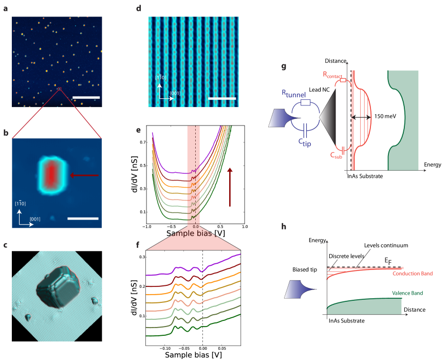
In this work, the Pb NCs are obtained by thermal evaporation of a nominal 0.3 monolayer of Pb on the (110) surface of InAs heated at C. The (110) surface is obtained by cleaving a n-type InAs substrate in ultra high vacuum at a base pressure mbar. Two distinct samples (A and B) have been prepared with slightly different NC concentrations and sizes. The volume of the NCs ranges from 20 nm to 800 nm while the height ranges from 1 unit cell (0.495 nm) to 5.2 nm, see Supplementary Fig. 2 and Supplementary Note 1 for details on NC volume determination. The scanning tunneling microscopy (STM) topographic images, Fig. 1abc and Supplementary Fig. 3, for sample A and sample B, respectively, show that Pb grows in the Volmer-Weber, i.e. island mode[18]. The 3D Laplacian image , Fig. 1c, shows that the NCs are well crystallized and expose mostly the (111) planes of the cubic face-centered Pb structure, as indicated by the observation of the characteristic hexagonal shape of the (111) facets. Surrounding these NCs, the surface remains free from adsorbate, as atomic resolution images of the (110) InAs surface prove, Fig. 1d.
0.2 Tip-induced QDot on the InAs surface
Fig. 1e shows the Differential Conductance (DC) measured on the InAs surface at several distances, from 0 to 10 nm, of a Pb NC. The data are measured at K, unless indicated otherwise, using a standard lock-in procedure (See Methods). The data indicate that the Fermi level is in the conduction band of InAs as expected for this n-doped sample. With a sulphur dopant concentration, cm-3, the Fermi level is 21 meV above the conduction-band minimum. A zoom on these spectra, Fig. 1f, shows multiple peaks that result from the discrete levels of the tip-induced Quantum Dot (QDot), a phenomena that has also been observed in previous works[19]. This demonstrates that Pb deposition on InAs do not produce any significant defects and doping. Indeed, in presence of defects or adsorbate, the surface of III-V semiconductors present interface states that pin the Fermi level at the charge neutrality level[20, 21], Fig. 1g. For InAs, this level is located 150 meV above its conduction band minimum, which leads to the formation of an electron accumulation layer as shown by numerous photoemission experiments[20, 22]. In contrast, perfectly clean (110) surfaces do not present any interface states and consequently the Fermi level is not pinned. Thus, the electric field from the STM tip can easily shift the conduction band and generates the so-called tip-induced QDot[19], as sketched Fig. 1h. While the energy of the QDot levels can shift on long distances, see Supplementary Fig. 4, as a consequence of variations in the electrostatic environment due to the random distribution of Pb NCs and sulphur dopants, we see, Fig. 1f, that the QDdot levels are not altered on short distances ( 10 nm) near the NCs. Only a weak broadening of the QDot levels is observed, likely a consequence of their weak tunnel coupling with the Pb NCs.
0.3 Coulomb blockade and nature of the tunnel barrier
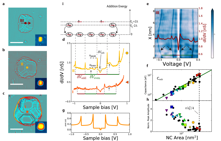
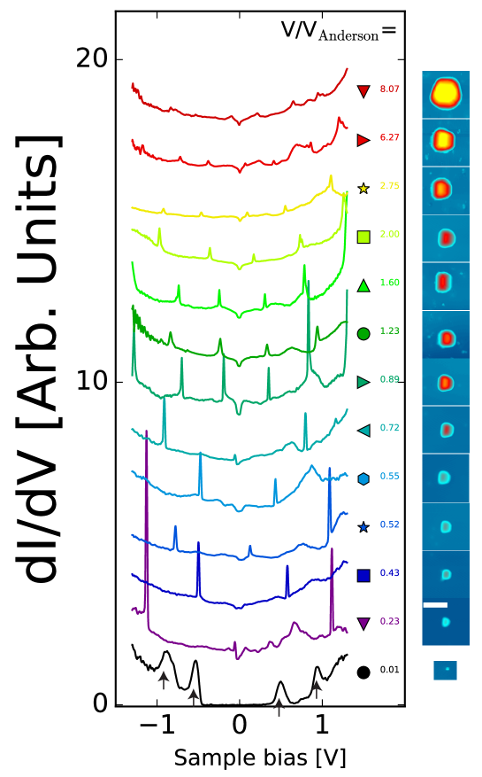
On NCs of three distinct sizes shown Fig. 2abc, representative DC spectra are shown Fig. 2de. They display a Coulomb gap at zero bias of width where () is the capacitance between the NC and the substrate (tip). The data also display sharp Coulomb peaks where the voltage interval between the peaks provides the addition voltage for an electron, which is related to the addition energy by : where is the arm lever; see Methods section for a derivation of these relations. Furthermore, the DCs may also display broad additional peaks, of weak amplitude in large NCs, , as indicated by arrows in Fig. 2d, but of large amplitude in small NCs, , as indicated by arrows in Fig. 3. These broad peaks are the signature of quantum well states in the Pb NCs due to strong confinement in the direction as observed in scanning tunneling studies of thin layers of Pb[23].
The color map Fig. 2e shows that changes slightly with the tip position above the NC, as consequence of the variation in the tip-NC capacitance . Fig. 3 shows the DCs for 13 additional NCs, from which the capacitance is extracted and shown as colored symbols in Fig. 2f and Supplementary Fig. 5. On these last plots, data points shown as black circles of 24 other NCs are also included, for which the DCs are not shown. Fig. 2f shows that increases linearly with the area as , using = 12.3, the dielectric constant of InAs and = 4 nm for the effective tunnel barrier thickness.
As no dielectric insulator has been deposited on the surface and no Schottky barrier exists at metal-InAs interfaces[21, 22], the origin of the tunnel barrier and the meaning of the thickness appear clearly only after one realizes that the Fermi wavelength of the 2D gas in InAs is larger than the lateral size of the NCs. At the interface between the Pb NC and InAs, the Fermi energy in InAs is at the charge neutrality level, meV, Ref. [21, 22], which gives for the Fermi wavelength nm. As known from numerous works with quantum point-contacts formed in 2D electron gas[24, 25], the transmission coefficient decreases for constrictions smaller than the Fermi wavelength. Because a NC covers only a fraction of the area , its transmission coefficient with the 2D gas is significantly smaller than one, which explains the observation of the Coulomb blockade. For a small NC, the weak coupling model Ref. [26] can be used to describe the data, as shown Fig. 2g. This model shows that the contact impedance is of the order of M, implying that the transmission coefficient is weak as anticipated. In this model, the magnitude of the Coulomb peaks increases with the ratio , as observed on the DC curves measured as function of tip height, Supplementary Fig. 6. Fig. 2h shows the amplitude of the Coulomb peak, normalized to its base value, as function of NC area. The amplitude is constant for small area ( 100 nm2) but decreases quickly for area approaching nm2. This behavior cannot be described by the weak-coupling model just discussed, however, it can be understood by considering models of Coulomb blockade in the strong coupling regime[27, 28]. These models show that the Coulomb oscillations disappear when approaches unity, when charge fluctuations between the NC and the substrate become significant. Fig. 3 shows that the Coulomb peaks of the largest NCs have almost completely disappeared. The fact that the amplitude of the Coulomb peaks decreases for NCs area approaching confirms our interpretation that the tunnel barrier is due to a quantum constriction of the electronic wave function at the interface between the NC and the 2D gas. Thus, the dielectric thickness = 4 nm extracted from above is actually set by the Debye length of the 2D gas and actually corresponds to the quantum capacitance of InAs.
0.4 Superconducting parity effect
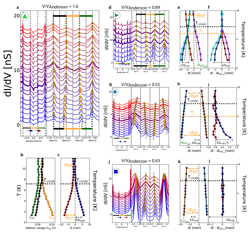
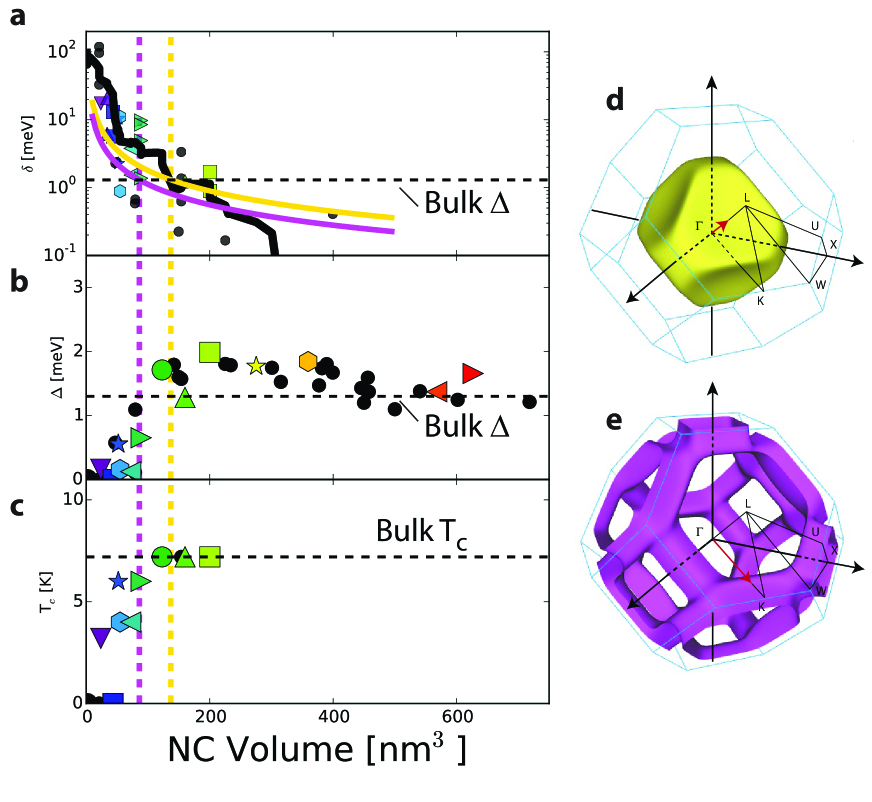
Thanks to this highly clean type of tunnel junction, free from quasi-particle poisoning, the superconducting parity effect in the NCs can be observed through the even-odd modulation of the addition voltage, as shown Fig. 2de, Fig. 3 and Fig. 4. The addition voltages can be precisely extracted thanks to the sharpness of the Coulomb peaks, which voltage positions are obtained through a fit with a Lorentz function, Supplementary Fig. 7. As sketched Fig. 2i and shown by Eq. 1, the addition voltage for injecting an electron in an even parity NC is higher than for injecting an electron in an odd parity NC, where the energy difference is given by the binding energy of the Cooper pair. Fig. 4a shows the DCs for a large NC, = 1.6, as function of temperature. The corresponding addition voltages, shown Fig. 4b, are almost equal above K, the superconducting transition temperature of bulk Pb. However, an even-odd modulation is observed at low temperature K. The difference in the addition energies between two successive charge configurations is obtained from . For this large NC, four Coulomb peaks are observed which provide three distinct addition voltages indicated by the horizontal bars. From these addition voltages, two distinct values of the addition energy difference between two charge configurations are obtained and given by , where the head (tail) refers to the colored arrows in the panel. These two values of are shown Fig. 4c as function of temperature. Their values is near zero at high temperature, , and increase below K to reach, at low temperature, the theoretically expected value , Ref. [1], where meV is the superconducting gap of bulk Pb. The value changes sign as one goes from the difference between two addition energies to the next difference .
For NCs smaller than the Anderson volume, Fig. 4dgj, we observe that is non-zero, which indicates that the electronic level spacing has now a significant contribution to the addition energy, following Eq. 1. The values of are distinct between successive charge configurations. Indeed, in metallic systems, the electronic levels are randomly distributed as described by Random Matrix Theory (RMT)[29]. Collecting the values for all NCs, Fig. 5a shows that, in average, the evolution of with NC volume can be properly described by the relation:
| (2) |
using m∗=1.2 me for the effective mass, where =7.01 nm-1 and =11.21 nm-1 are characteristic wave-vectors of the two Fermi surfaces FS1 and FS2 of Pb.
For the NC of volume = 0.89, Fig. 4d, while the level spacing is large, the shift of the Coulomb peaks due to the parity effect is still dominating the temperature dependence and can be observed directly on the raw data and the addition energy difference plotted as function of temperature on Fig. 4e. A line is extrapolated from high temperature and the difference gives the temperature dependence of the superconducting gap, Fig. 4f, which shows that the critical temperature K is smaller than the bulk value. The amplitude of the superconducting gap is obtained from . For this NC, the superconducting energy gap is about two times smaller than the bulk value, .
For the smaller NC of volume = 0.55, Fig. 4g, the level spacing is larger and has a temperature dependence that dominates the shift of the Coulomb peaks with temperature. This shift could be the consequence of thermally induced electro-chemical shifts or temperature dependent strain or electric field effects. While the parity effect is barely visible on the raw data, using the procedure employed for the previous NC, the temperature K value and the energy gap can be extracted, Fig. 4i.
Finally, for the smallest NCs = 0.43 (0.34), shown respectively Fig. 4j and Supplementary Fig. 8h, they have the largest level spacing and, even though the addition energies are measured with much higher resolution than the superconducting gap energy, no parity effect can be observed on Fig. 4l and Supplementary Fig. 8j, respectively.
For 13 NCs where the DCs have been acquired as function of temperature, some of which are shown Fig. 4 and Supplementary Fig. 8, the level spacing, the superconducting gap energy and the transition temperature are extracted and plotted Fig. 5a, Fig. 5b and Fig. 5c, respectively. Upon reducing the NC volume, both quantities display a sharp decrease to zero when the level spacing becomes of the order of the superconducting gap energy, 1 meV. See Supplementary Note 2 for a comparison with the results of Bose et al.[17] on a system where the superconducting nanoparticles are strongly coupled to the normal substrate.
Discussion
Fig. 5 suggests that superconductivity disappears when the mean level spacing at the Fermi surface of the electron-type band, Fig. 5e, increases up to the superconducting gap energy. This is consistent with recent theoretical calculations [30] and STM measurements[31] which have shown that electron-phonon coupling is stronger for this electron-type band owing to its p-d character. Regarding the BCS ratio, within the experimental resolution, no significant deviation from the bulk value has been observed.
To summarize, we have found that a 2D electron gas of large Fermi wavelength constitutes an ideal substrate for studying Coulomb blockade in nanosized NCs evaporated in an ultra-high vacuum environment. This discovery leads us to observe, for the first time by STM, the parity effect and quantum confinement in isolated superconducting NCs and enabled the first demonstration of the Anderson criterion for the existence of superconductivity at single NC level. Furthermore, this new insight on the superconductor-InAs interface is of interest for topological superconductivity where Majorana islands are generated by depositing a superconductor on InAs nanowires[32, 33].
0.5 Relation between sample bias and energies
The Coulomb gap at zero bias results from Coulomb blockade that prevent charge fluctuations in the NC. As sketched in Supplementary Fig. 1, Coulomb blockade is lifted when the Fermi level of either one of the electrodes is aligned with one of the excited levels of the NC. Thus the amplitude of the Coulomb gap observed in the DC is given by =2, with .
The Coulomb peaks observed at higher voltages result from the shift of the electrochemical potential of the NC upon increasing the voltage bias across the double junction. This shift is given by :
| (3) |
with :
| (4) |
Charge states with increased number of electrons become accessible when the electrochemical potential changes by . Thus the voltage difference between two charge states is given by :
| (5) |
This formula shows that the addition voltage depends only on the capacitance C and not on the capacitance C, as shown Supplementary Fig. 1b, where a simulation of the conduction spectrum, using the Hanna and Tinkham model[26] for two distinct values of the capacitance C.
0.6 Addition energies
The electrochemical potential of a nanocrystal with an even (odd) N (N+1) number of electrons is given by:
From these last equations, one obtains the addition energies for a NC with an even (odd) N (N+1) number of electrons :
Thus, the difference of addition energies between two successive charge states is given by :
| (9) |
When the electronic spectrum of the NC is discrete, the level spacing should be included in the addition energy.
| (11) |
0.7 Random level distribution
In metallic NCs, the electronic level distribution is described by RMT[29, 35]. In a NC with strong spin-orbit coupling, RMT predicts that the level spacing should be described by a Gaussian symplectic ensemble. For this level distribution, shown Supplementary Fig. 9, the width of the distribution, i.e. the standard deviation, is equal to ,[29, 36]. Between two successive charge states, the addition energy can fluctuate by an amount of the order of , consequently, in average, the difference in addition energies between two successive charge states is given by:
| (13) |
At temperatures above the superconducting transition temperature:
| (15) |
Thus an estimation of the level spacing can be obtained by a measure of the difference in the addition energies above .
Furthermore, the gap amplitude can be obtained from:
| (17) |
0.8 Measurements details
The microscope used is a low temperature, K, Joule-Thomson JT-STM from SPECS accommodated with a preparation chamber operating in Ultra High Vacuum at a base pressure mbar. The differential conductance curves dI/dV are measured with a standard lock-in procedure. An AC signal of amplitude about 1 meV and frequency about 777 Hz is employed.
0.9 Data avaibility
The data that support the main findings of this study are available from the corresponding author upon request.
0.10 References
References
- [1] Averin, D. V. & Nazarov, Y. V. Single-electron charging of a superconducting island. Physical Review Letters 69, 1993–1996 (1992).
- [2] Lafarge, P., Joyez, P., Esteve, D., Urbina, C. & Devoret, M. H. Two-electron quantization of the charge on a superconductor. Nature 365, 422–424 (1993).
- [3] Tuominen, M. T., Hergenrother, J. M., Tighe, T. S. & Tinkham, M. Experimental Evidence for Parity-Based 2e Periodicity in a Superconducting Single-Electron Tunneling Transistor. Physical Review Letters 69, 1997–2000 (1992).
- [4] Eiles, T., Martinis, J. & Devoret, M. Even-odd asymmetry of a superconductor revealed by the Coulomb blockade of Andreev reflection. Physical Review Letters 70, 1862–1865 (1993).
- [5] Lafarge, P., Joyez, P., Esteve, D., Urbina, C. & Devoret, M. H. Measurement of the even-odd free-energy difference of an isolated superconductor. Physical Review Letters 70, 994–997 (1993).
- [6] Higginbotham, A. P. et al. Parity lifetime of bound states in a proximitized semiconductor nanowire. Nature Physics 1–6 (2015).
- [7] Joyez, P., Lafarge, P., Filipe, A., Esteve, D. & Devoret, M. H. Observation of parity-induced suppression of Josephson tunneling in the superconducting single electron transistor. Physical Review Letters 72, 2458–2461 (1994).
- [8] Aumentado, J., Keller, M. W., Martinis, J. M. & Devoret, M. H. Nonequilibrium Quasiparticles and 2 e Periodicity in Single-Cooper-Pair Transistors. Physical Review Letters 92, 066802 (2004).
- [9] van Woerkom, D. J., Geresdi, A. & Kouwenhoven, L. P. 1 minute parity lifetime of a NbTiN Cooper-pair transistor. Nature Physics 11, 1–5 (2015).
- [10] Anderson, P. Theory of dirty superconductors. Journal of Physics and Chemistry of Solids 11, 26–30 (1959).
- [11] Ralph, D. C., Black, C. T. & Tinkham, M. Spectroscopic Measurements of Discrete Electronic States in Single Metal Particles. Physical Review Letters 74, 3241–3244 (1995).
- [12] von Delft, J. & Ralph, D. Spectroscopy of discrete energy levels in ultrasmall metallic grains. Physics Reports 345, 61–173 (2001).
- [13] Reich, S., Leitus, G., Popovitz-Biro, R. & Schechter, M. Magnetization of Small Lead Particles. Physical Review Letters 91, 147001 (2003).
- [14] Zolotavin, P. & Guyot-Sionnest, P. Meissner effect in colloidal Pb nanoparticles. ACS nano 4, 5599–608 (2010).
- [15] Savin, A. M. et al. Parity effect in Al and Nb single electron transistors in a tunable environment. Applied Physics Letters 91, 063512 (2007).
- [16] Hong, I.-P., Brun, C., Pivetta, M., Patthey, F. & Schneider, W.-D. Coulomb blockade phenomena observed in supported metallic nanoislands. Frontiers in Physics 1, 1–8 (2013).
- [17] Bose, S. et al. Observation of shell effects in superconducting nanoparticles of Sn. Nature materials 9, 550–554 (2010).
- [18] Brune, H. Microscopic view of epitaxial metal growth: nucleation and aggregation. Surface Science Reports 31, 125–229 (1998).
- [19] Dombrowski, R., Steinebach, C., Wittneven, C., Morgenstern, M. & Wiesendanger, R. Tip-induced band bending by scanning tunneling spectroscopy of the states of the tip-induced quantum dot on InAs(110). Physical Review B 59, 8043–8048 (1999).
- [20] Tersoff, J. Theory of semiconductor heterojunctions: The role of quantum dipoles. Physical Review B 30, 4874–4877 (1984).
- [21] Mönch, W. Semiconductor surfaces And Interfaces (Springer Berlin Heidelberg, 2001).
- [22] Morgenstern, M. et al. Scanning tunneling microscopy of two-dimensional semiconductors: Spin properties and disorder. Physica E: Low-dimensional Systems and Nanostructures 44, 1795–1814 (2012).
- [23] Su, W. B. et al. Correlation between Quantized Electronic States and Oscillatory Thickness Relaxations of 2D Pb Islands on Si(111)-( 7 × 7 ) Surfaces. Physical Review Letters 86, 5116–5119 (2001).
- [24] van Wees, B. J. et al. Quantized conductance of point contacts in a two-dimensional electron gas. Physical Review Letters 60, 848–850 (1988).
- [25] Pasquier, C. et al. Quantum limitation on Coulomb blockade observed in a 2D electron system. Physical Review Letters 70, 69–72 (1993).
- [26] Hanna, A. E. & Tinkham, M. Variation of the Coulomb staircase in a two-junction system by fractional electron charge. Physical Review B 44, 5919–5922 (1991).
- [27] Matveev, K. A. Coulomb blockade at almost perfect transmission. Physical Review B 51, 1743–1751 (1995).
- [28] Aleiner, I., Brouwer, P. & Glazman, L. Quantum effects in Coulomb blockade. Physics Reports 358, 309–440 (2002).
- [29] Alhassid, Y. The statistical theory of quantum dots. Reviews of Modern Physics 72, 895–968 (2000).
- [30] Floris, A., Sanna, A., Massidda, S. & Gross, E. K. U. Two-band superconductivity in Pb from ab initio calculations. Physical Review B 75, 1–6 (2007).
- [31] Ruby, M., Heinrich, B. W., Pascual, J. I. & Franke, K. J. Experimental Demonstration of a Two-Band Superconducting State for Lead Using Scanning Tunneling Spectroscopy. Physical Review Letters 114, 157001 (2015).
- [32] Das, A. et al. Zero-bias peaks and splitting in an Al–InAs nanowire topological superconductor as a signature of Majorana fermions. Nature Physics 8, 887–895 (2012).
- [33] Albrecht, S. M. et al. Exponential Protection of Zero Modes in Majorana Islands. Nature 1, 1–6 (2015).
- [34] Kouwenhoven, L. P., Austing, D. G. & Tarucha, S. Few-electron quantum dots. Reports on Progress in Physics 64, 701–736 (2001).
- [35] Halperin, W. Quantum size effects in metal particles. Reviews of Modern Physics 58, 533–606 (1986).
- [36] Mehta, M. L. Random Matrices (Academic Press, 2004).
We acknowledge fruitful discussions with M. Aprili, C. Delerue and B. Grandidier. H.A., A.Z. acknowledge support from ANR grant ”QUANTICON” 10-0409-01, ANR grant ”CAMELEON” 09-BLAN-0388-01, China Scholarship Council and labex Matisse. DR and SP acknowledge C’NANO Ile-de-France, DIM NanoK, for the support of the Nanospecs project.
H.A. proposed the experiment. C.D., G.R., J.C.G designed the STM holder and prepared the InAs substrates. S.V., S.P., T.Z. and H.A. evaporated the lead nanocrystals on the cleaved InAs substrate and carried out the STM measurements with the help of D.R. H.A. analyzed the data and wrote the manuscript with the help of all authors.
The authors declare that they have no competing financial interests.
Correspondence and requests for materials should be addressed to H.A. (email: herve.aubin@espci.fr)