Algorithms for Embedding Quantum-Dot Cellular Automata Networks onto a Quantum Annealing Processor.
Abstract
Advancements in computing based on qubit networks, and in particular the flux-qubit processor architecture developed by D-Wave System’s Inc., have enabled the physical simulation of quantum-dot cellular automata (QCA) networks beyond the limit of classical methods. However, the embedding of QCA networks onto the available processor architecture is a key challenge in preparing such simulations. In this work, two approaches to embedding QCA circuits are characterized: a dense placement algorithm that uses a routing method based on negotiated congestion; and a heuristic method implemented in D-Wave’s Solver API package. A set of benchmark QCA networks is used to characterise the algorithms and a stochastic circuit generator is employed to investigate the performance for different processor sizes and active flux-qubit yields.
Index Terms:
Quantum cellular automata, heuristic algorithms, quantum dots, quantum computingI Introduction
Quantum-dot cellular automata (QCA) is a computational nanotechnology that employs a 2D patterned array of charge or magnetically coupled finite-state devices, QCA cells, for both classical and potentially quantum computing. There have been several experimental demonstrations of this technology in tunnel coupled metal-islands [1], patterned nanomagnets [2], and silicon-on-insulator [3] including recent work in mixed-valence molecules [4, 5, 6] and atomic scale QCA built with charge coupled silicon dangling bond quantum dots [7]. Theoretical work on QCA was started by C.S. Lent et al, in 1993 with a seminal paper introducing the 5-dot QCA cell and QCA ground state computing [8]. QCA networks have been predominantly treated using a Ising spin-glass model as it has been shown that the state of a properly operating binary QCA device remains relatively well described in the two-state approximation [9]. While a full quantum mechanical treatment scales as , where is the number of cells, Tóth et al. showed theoretically that long-range correlations and entanglement between QCA cells was not necessary in reproducing QCA network dynamics [10].
QCA operation is fundamentally a quantum annealing process, with each component of a QCA circuit designed such that the ground state yields the desired output logic. Clocking is necessary in order to enforce directionality of information flow through the circuit and is achieved by controlling the cell parameters such that in the two-state approximation there is an effective modulation of the tunnelling between the polarization states [11]. So-called “clocking-zones” are sections of the circuit with cells assigned identical tunnelling in each clock phase. The cells in each subsequent clocking-zone are transitioned from their unpolarized “relaxed” state with strong tunnelling, to a polarized “latched” state with weak tunnelling. This is analogous to the usual quantum annealing procedure, in which a state is driven to its ground state by reducing the relative strength of the inter-state tunnelling. This suggests that some insight might be gained into the performance of QCA circuits by investigating an analogous quantum annealing architecture. In particular, such an architecture could probe the impact of coherent and environmental contributions to the dynamics during QCA clocking,
Work by D-Wave Systems Inc. in Burnaby Canada to realize a large scale quantum annealing platform [12, 13] has made it possible to explore the application of quantum annealing to the quantum simulation of large QCA circuits. The two-state approximation of QCA cell interactions and the interactions of qubits in D-Wave’s quantum annealing processor (QAP) both produce governing Hamiltonians of analogous form. With a suitable embedding, the cell polarizations of a QCA circuit map directly to the expectations of qubit spins. However, the number of qubits on the QAP is limited and presently each qubit only couples to at most six other qubits. The sparse connectivity means that it is generally not possible to embed larger circuits using a one to one mapping between individual qubits and QCA cells. Additional qubits are needed to facilitate all interactions, with multiple qubits representing a single QCA cell. The choice of these multi-qubit groups defines the embedding of a QCA circuit. It is not yet clear how these additional qubits contribute to the statistics of the quantum annealing process for a QCA circuit or what effect they have on the expected ground state.
In Section II, we provide a brief overview of the theoretical principles of QCA cells and the flux-qubits as implemented in D-Wave’s architecture. In particular, we comment on the analogous form of cell-cell and qubit-qubit interaction Hamiltonians in the two-state approximation. In Section III, we discuss the problem of embedding and present two approaches to finding QCA circuit embeddings. In Section IV, we present embedding results using benchmarks circuits and use a stochastic circuit generator to estimate the range of circuits that can be successfully embedded onto different processor sizes, with a focus on the 512 qubit “Vesuvius” QAP. An earlier version of this paper was presented at COMMAD 2014 [14]. In this expanded work, we discuss aspects of the algorithm implementations and extend our analysis to better characterise the embedding algorithms over a range of processor sizes and yields.
II Theoretical Background
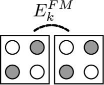
In the two-state approximation, cell-cell interactions are determined by an interaction energy, , referred to as the kink energy. The kink energy is defined as the change in electrostatic energy when two cells are switched from the same to opposite polarizations. This energy is a function only of the cell geometries and not the cell polarizations themselves. Typical arrangements for interacting 4-dot QCA cells are shown in Fig. 1. In keeping with the terminology used in Ising spin-glass models we use ferromagnetic and anti-ferromagnetic to refer to interactions that preferentially result in the same or opposite polarizations respectively. A layout of such QCA cells has an Ising-like Hamiltonian [15],
| (1) | |||||
where is an effective tunnelling energy, is the kink energy between cells and , is the polarization of driver , is the kink energy between cell and driver and are the Pauli operators for the cell with . For the configurations shown in Fig. 1, the kink energies with respect to an energy scale can be determined to be and for ferromagnetic and anti-ferromagnetic interactions respectively.
D-Wave’s processor uses interacting superconducting flux qubits and has an operational Hamiltonian approximately of the form [16]
| (2) | |||
| (3) |
where and are time dependent energy scales that define the annealing schedule and and are constants which describe a given Ising spin type optimization problem. Letting be the annealing time, the eigenspectrum after annealing can be made equal to that of a QCA circuit by setting
The and are dimensionless variables with values in the interval . As the are typically small for latched clocking zones, it is appropriate to allow which simplifies qubit readout. There is in general some error in assignment of and values so it is preferable to scale the and to have maximum magnitude in order to minimize the relative error. In practice, this means scaling by such that is the interaction strength between ferromagnetically coupled QCA cells.
III Embedding
Given a configuration of QCA cells, we aim to find a set of qubits and couplers such that the ground state achieved by quantum annealing maps to the ground state polarizations of the QCA circuit. In this section we discuss the convenience of representing QCA circuits as connectivity graphs, give an interpretation of the additional qubits necessary in embedding to facilitate the full set of interactions, describe the two embedding methods, and describe a method for converting the solutions to a form useful for parameter assignment and state readout after annealing.
III-A Graph Representation
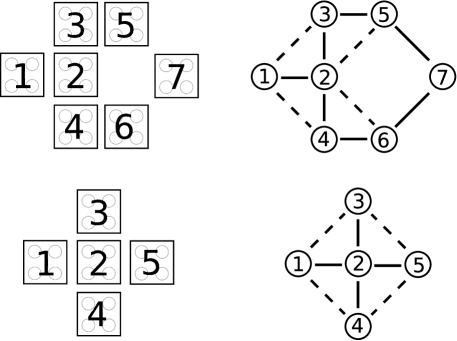
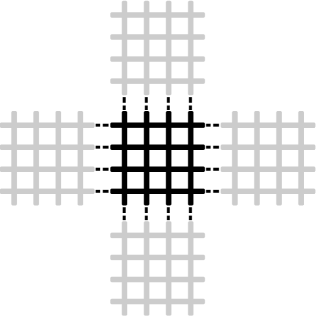
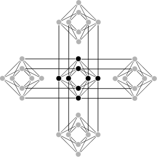
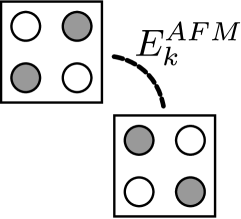
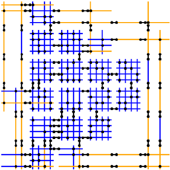
For the purpose of consistent discussion, it is convenient to represent the cell interactions of a QCA circuit via a connectivity graph with driver cell contributions and cell-cell interactions mapping to node and edge weights respectively. As the quadrupole-quadrupole interaction between cells is approximately proportional to , where is the distance between cell centers, we consider only the interactions between cells within a radius of less than two cell sizes. The connectivity graph representations of the two fundamental QCA logic gates are shown in Fig. 2. We define limited adjacency as including diagonal (anti-ferromagnetic) cell interactions only in the case of an inverter and full adjacency as when diagonal cell interactions are included for all cells. With this representation, the problem of embedding translates to finding the connectivity graph of the QCA circuit as a minor in the “Chimera” graph (single tile shown in Fig. 3), which describes the available connections on D-Wave’s QAP [17].
III-B Virtual QCA Cells
Due to present constraints on connectivity, additional qubits are sometimes requires in order to accommodate all the relevant QCA network interactions. We can interpret these additional qubits within the framework of a QCA circuit as “virtual” QCA cells; these virtual cells, which do not exist in the original circuit, are inserted between “real” QCA cells to facilitate all original interactions.
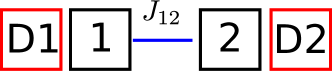
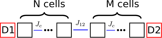
As a simple model to understand the effects of these virtual cells or qubits we consider the single cell-cell interaction as shown in Fig. 4a. Here the driver cells on either side of the cells can represent an ICHA-like approximation of the coupling to the rest of the QCA circuit. The coupling strength between the two cells is indicated by . We are interested in quantifying the effect of replacing each cell in the cell-cell interaction model by a group of coupled cells. Such a representation can be seen in Fig. 4b with internal coupling strength, , between the cells inside each group as indicated. will in general represent a strong ferromagnetic interaction.
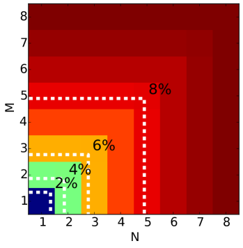
As a metric for estimating the effect of such a replacement, we observe that in adiabatic annealing the probability of a non-adiabatic state evolution during an avoided crossing falls off as the minimum energy gap increases between the ground and first excited states [18, 19]. As adding more cells generally decreases the energy gap, we consider the percent reduction in the energy gap resulting from replacing the two cells by groups of size and respectively. In Fig. 5, we consider these results both for the strong ferromagnetic () and weak anti-ferromagnetic () interactions common in QCA networks. Here we have used driver polarizations which would be expected for the given interactions: for ferromagnetic coupling and for anti-ferromagnetic coupling. The stronger the internal coupling strength relative to the interaction strength between cell groups, the more accurately each cell group will match the behaviour of a single cell. As the parameter range for and is fixed, the strongest interaction we can achieve is . An effectively stronger can be achieved by reducing all and inter-group parameters by a constant factor however this would increase the relative error arising from parameter assignment accuracy on the processor. Observe that for the boundary between the two groups is arbitrary and thus the energy gap can depend only on the total number of cells. If the coupling strength is weaker than the internal coupling as in we observe that the energy gap approximately depends only on the maximum group size. As a general rule for either case, it is preferable to arrange the allocation of virtual cells or qubits in order to minimize the largest group size. The simulated percent decrease in the energy gap remained less than 10% for group sizes up to 8 cells (16 cells total). These simple considerations suggest a minimal effect for small group sizes. Other effects such as interactions with the environment will likely make large virtual cell groups not perform as expected but we assume such effects are similarly limited for sufficiently small maximum group sizes.
III-C Dense Placement Embedding Algorithm
The Dense Placement algorithms uses a simultaneous “place-and-route” approach commonly used in FPGA design [20]. It attempts to place every node in the QCA connectivity graph onto a corresponding assigned qubit in the Chimera graph. Interactions between cells are facilitated either by direct coupling or by chains of qubits routed between these assigned qubits.
III-C1 Initial Seed
Before the main loop can be called, an initial seed must first be selected. The first QCA cell node and its corresponding qubit are chosen as follows. Each QCA cell is assigned a probability proportional to where is the number of neighbours of cell and is a constant. In this paper, was selected to be 3 in order to prioritize high adjacency cells but still allow some chance for lower adjacency cells to be selected. In selecting the seed qubit, each tile is assigned a probability according to a Gaussian distribution about the center of the tile array with width . The qubits of that tile are then randomly ordered and iterated through until a qubit is found with enough neighbours to facilitate the interactions of the selected seed cell. If no such qubit is found, a new tile is selected. In this work, was chosen to be 1 to strongly bias initial placement near the center of the Chimera graph.
III-C2 Cell Placement
Building from the initial seed, for each iteration of the main loop we look at the set of unplaced cells adjacent to the set of placed cells and sort by decreasing number of unplaced connections. For each cell to be placed, we aim to select a qubit with sufficiently many available neighbouring qubits to facilitate all interactions. Such a qubit is referred to as suitable. The chosen qubit is that which is both suitable and yields the shortest total path to all qubits assigned to adjacent cells. This is achieved by simultaneously running a lowest cost path search from each such qubit until a suitable qubit is reached by all search trees. The cost of each edge in the search contains two components: a contribution from the type of coupling to the new node (internal or external to a tile), and an edge proximity contribution which weighs nodes in tiles closer to the edge of the processor more strongly. For dense placement, internal tile placements are preferred so internal couplers have lower cost than external couplers. The external coupler cost was chosen to be times the internal coupler cost such that one external coupler was preferable to two internal couplers. The edge proximity cost increases linearly as the minimum distance to the processor edge decreases. An increase in cost of 0.5 per tile was chosen for the 512 qubit processor. These parameters were chosen to tightly pack long chains of low adjacency cells and avoid running out of room for embedding.
III-C3 Routing
The routing algorithm is based on negotiated congestion, a well established path finding technique used in mapping netlists to FPGAs [20]. This method aims to minimize the path length for each route by use of a cost scheme that penalizes the use of a qubit for more than one path.
III-C4 Seam Opening
In the case that there is no suitable qubit available, the translational symmetry of the chimera graph allows an avenue of qubits and couplers to be “opened” by shifting all qubits after or before a row or column. We interpret this as opening a seam between two rows or columns. As specific qubits or couplers may be inactive due to manufacturing yield, some shifted qubits may require remapping. Such qubits are said to “conflict”. Following such a shift, remapping is achieved by finding new placements for cells with conflicting assigned qubits and rerouting conflicting paths. The new cell placements can result in recursive calls to seam opening and remapping. A basic metric for selecting which seam to open and in which direction is used. For the given cell to be placed, we consider all seams adjacent to assigned qubits of the cell’s placed neighbours. For each of these seams and each opening direction, we check that there is a free row or column to shift into. If so, we assign to that seam a cost, , given by
| (4) |
where and are the number of conflicting assigned qubits and paths, is the seam distance defined as the minimum distance between the seam and the mean location of all assigned qubits, and , , and are the relevant cost factors. In this work, the cost factors were chosen as , , and . Typically, fewer qubits were needed for replacing a small number of qubits than re-routing a number of paths.
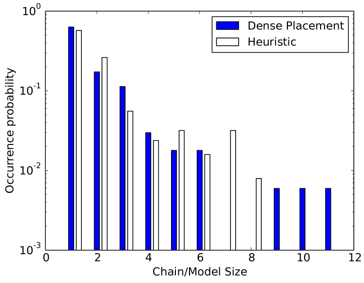
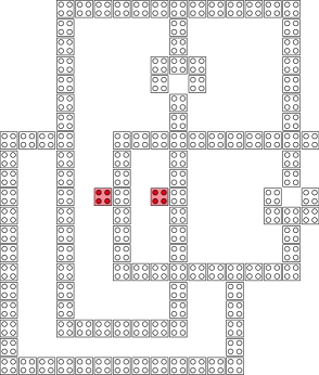
The Dense Placement algorithm is good at keeping most routes between mapped qubits to only one or two couplers. However, as the placement builds outwards from the center and does not currently account for how the final cells to be placed are connected, there are often long chains of ten or more qubits about the perimeter of the embedding needed to facilitate the final connections. Fig. 6 shows an example distribution of qubit chain lengths for an embedding of a serial adder. The QCA cell layout and a sample embedding for the serial adder are shown in Fig. 7. Note the long chains about the perimeter as discussed.
III-D D-Wave’s Heuristic Embedding Algorithm
D-Wave’s Solver API package includes an embedding solver which uses a heuristic method to attempt to find a source graph as a minor in the hardware connectivity graph. For each node in the source graph, the heuristic algorithm attempts to find a connected sub-graph or “vertex-model” comprised of strongly coupled qubits. Edges between nodes in the source graph translate to shared edges between vertex-models in the Chimera graph. A detailed description of this algorithm can be found elsewhere [21] but the basic approach is provided here.
For each node in the source graph, assign an initial vertex-model as follows. If none of the current node’s neighbours have been assigned a vertex-model, randomly select a qubit in the target graph as the vertex-model. Otherwise, find the qubit with the smallest total path cost to all of the adjacent vertex-models and assign this qubit as the root of the vertex-model. The same qubit can be used by multiple paths at a high cost. Paths to the adjacent vertex-models are distributed between vertex-models to minimize the largest vertex-model size. After initial placement, iteratively loop through each source node, forget the previously assigned vertex-model and try to find a better one. The metrics for improvement are defined as the number of times a single qubit is used in the set of all vertex-models (must be no more than once for a successful embedding), the sum of vertex-model sizes, and the largest vertex-model size.
This method is good at reducing the total number of qubits used and the largest group of qubits assigned to a single QCA cell. Refer to Fig. 6 for an example of the distribution of vertex-model sizes. As the number of short vertex-models are not considered, fewer small groups are typically found than short chains in the Dense Placement algorithm.
III-E Parameter Assignment and Model Conversion
Once an embedding is found, it is necessary to assign bias and coupler parameters and to the included qubits and couplers respectively. In the vertex-model representation, this is easily achieved. The vertex-model for QCA cell has a set of qubits, , connected by internal couplers and a set of external couplers which couple to each adjacent QCA cell vertex-model. The biases, , of the vertex-model must sum to the bias for the QCA cell. We distribute the bias uniformly as
| (5) |
The couplers between qubits within each model are all assigned the maximum ferromagnetic parameter . Typically there is only one coupler between each pair of vertex-models to which we assign the corresponding . If multiple couplers exist between two models, we can choose to uniformly distribute .
In the place-and-route representation, it is not so trivial to choose a scheme for parameter assignment. Between each pair of qubits assigned to adjacent QCA cells there can exist a chain of virtual qubits. The interaction term between the two cells can be assigned to any coupler along this chain without changing the effective interaction between the assigned qubits, given that all other connectors are assigned . The act of parameter assignment then takes the form, using the terminology so-far defined, of finding an effective vertex-model for each cell by deciding where along each virtual qubit chain to assign the interaction term. Once the vertex-models are found, we can proceed as above to assign bias and interaction parameters.
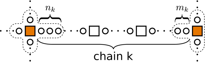
In Sec. III-B, it was suggested that the behaviour of two interacting vertex-models is optimized by minimizing the maximum vertex-model size. We assume this to be a general feature of any interacting network of vertex-models. One can formulate the allocation of virtual qubits with the aim to minimize the maximum of all vertex-model sizes as a linear optimization problem. First, in order to maintain the correct number of connectors between vertex-models observe that any cell with greater or less than 2 neighbours must contain in its vertex-model its assigned qubit. It is then useful to reinterpret the QCA circuit connectivity graph as a set of “end-node” () cells connected by chains of “internal-node” () cells. The Dense Placement algorithm then effectively constructs chains containing virtual and internal-nodes between the end-nodes. One such chain is illustrated in Fig. 8. Note that the internal-nodes could be placed anywhere along these chains without changing the embedding as long as their order is maintained. The problem of qubit allocation then reduces to determining the number of qubits at the end of each chain assigned to the vertex models of the end-nodes. The remaining qubits of each chain are divided evenly between the internal-node cells. Only chains containing virtual qubits need to be considered.
The chain contains internal-nodes and total of qubits, excluding the end-nodes. Of these qubits, and qubits are assigned to the vertex-models of the end-nodes at the beginning and end of the chain respectively. Then the chain has an average internal-node vertex-model size, , of
| (6) |
If is the sum of all , associated with the end-node, then each end-node has a vertex-model size, of
| (7) |
The linear programming problem is then given as minimizing the maximum of the set of all and with constraints and . This is an integer programming problem and hence is potentially computationally intensive. Typically the number and allowed range of parameters is small so this was not observed to be a concern. If necessary, linear programming (LP) relaxation can be used, removing the integer constraint on and , with some consideration to rounding in post-processing. This method optimizes the maximum vertex-model size but does not consider the distribution of the remaining vertex-models. Better results could be obtained from a non-linear optimization which considers all vertex-model sizes.
IV Embedding Results
We ran both algorithms on a variety of circuits to determine the number of qubits required for a given number of QCA cells. We used a set of benchmark circuits to investigate the performance on designed QCA circuits as well as implemented a stochastic circuit generator to gain insight into the range of embeddable circuits. In sections IV-A through IV-C, we assume no disabled qubits or couplers on the target processor.
IV-A Benchmark Circuits
| Circuit | Cells | Circuit | Cells |
|---|---|---|---|
| SR Flip Flop | 20 | Memory Loop | 120 |
| Selectable Oscillator | 31 | Serial Adder | 126 |
| XOR Gate | 73 | 4 Bit 2-1 Mux | 192 |
| Full Adder | 98 | 4 Bit Accumulator | 273 |
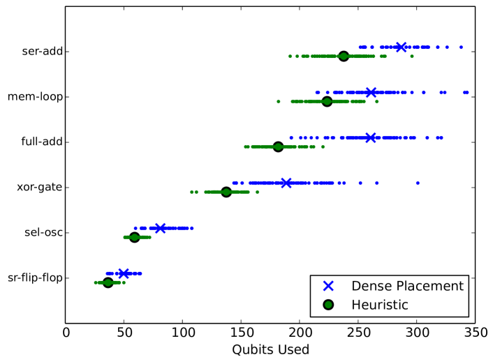
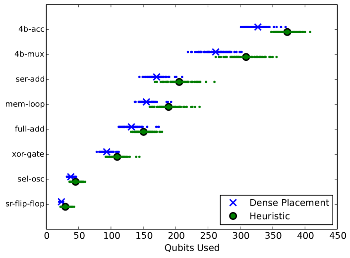
There were eight benchmark circuits used to test the embedding capabilities of the Dense Placement and Heuristic algorithms. The circuit names and numbers of non-driver cells are shown in Table I. None of the benchmark circuits contain crossover elements and the clocking arrangements were ignored. For each benchmark circuit, we attempted to find 100 embeddings using each algorithm for both limited and full adjacency. Fig. 9 shows the number of qubits needed for each circuit for both adjacency types.
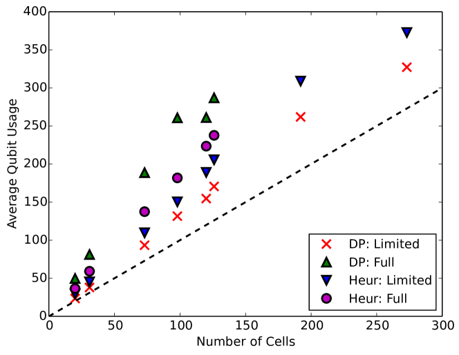
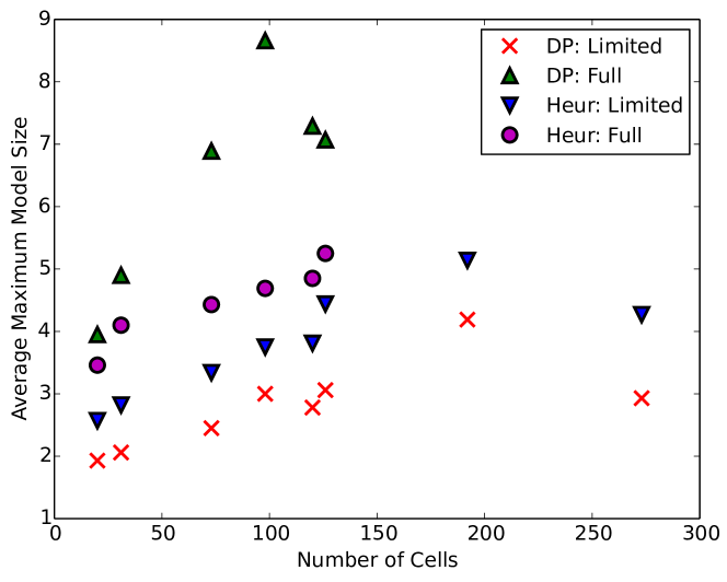
We observed that for full adjacency the Heuristic algorithm required fewer qubits whereas the Dense Placement algorithm required fewer qubits for limited adjacency. We also see that for each of the benchmark circuits, the Heuristic algorithm had a smaller reduction in qubit usage from full adjacency to limited adjacency than observed in the Dense Placement algorithm. This suggests that the Heuristic algorithm is much better than the Dense Placement algorithm at handling highly connected nodes but is not particularly efficient at embedding large numbers of sparsely connected nodes as is the case for limited adjacency. In contrast, the Dense Placement algorithm is good at tightly packing cells which have only one unplaced connection. In such cases it prioritizes same tile placement and hence condenses long wires into small regions of the Chimera graph. For comparison, a summary of the average qubit usages for the benchmark circuits for both methods and adjacencies is included in Fig. 10a. In all cases, the qubit usage seems to be approximately linear with circuit size. Fig. 10b. shows the average maximum vertex-model size with conversion for the Dense Placement results achieved as discussed in Sec. III-E. While the maximum model size tends to increase slightly with the number of cells it seems to be more a function of the complexity of the circuit. This can be seen with the 4-bit accumulator circuit which has the most cells, most of which exist in long wires, but has a lower maximum model size than many of the smaller circuits.
IV-B Generated Circuits
To understand what range of QCA circuits can be embedded within D-Wave’s architecture, it was necessary to implement a stochastic circuit generator which constructs QCA circuits with random numbers of primitive circuit components and connecting wire lengths. The generated circuits were made exclusively of inverters, majority gates, driver cells, and wires. Connecting wires are generated in the connectivity graph representation as random trees with the root at the output of a primitive component and each leaf at an input of another primitive component.
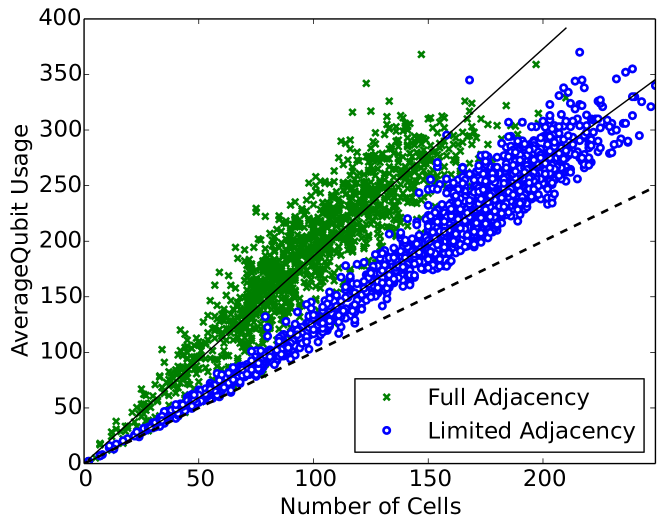
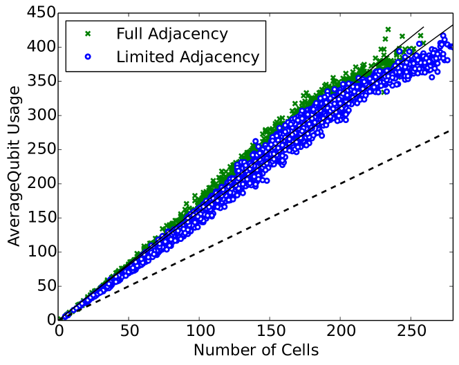
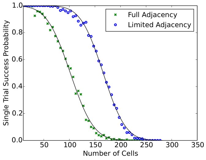
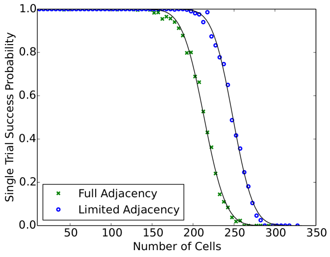
We generated 2000 circuits for both limited and full adjacency and attempted to find embeddings within a 512 qubit processor using both algorithms. Ten trials were run for each circuit with a maximum allowable run-time per trial of 30 seconds. Fig. 11 shows the average number of qubits used against the number of cells in the generated circuits for successful embeddings. Power function fits are included which indicate an approximately linear, or slightly super-linear in the case of the Dense Placement algorithm with limited adjacency, trend. As in the benchmark circuits, the Dense Placement algorithm performs better for limited adjacency than the Heuristic algorithm with the opposite true for full adjacency. Notably, the qubit usage in the benchmark circuit embeddings is consistent with the generated circuit data suggesting that the designed circuits are neither more nor less difficult to embed. The fall-off in qubit usage for the heuristic algorithm is likely a consequence of the circuit generator. Fig. 12 shows the average single trial embedding success probability as a function of the number of cells. It was observed that the success probability as a function of the number of cells, , is approximately of the form
| (8) |
with erfc the complementary error function, , and a measure of the width of the decline about . Fitted parameters are included in Table II. It is clear that even though the Dense Placement algorithm uses fewer qubits in limited adjacency, the Heuristic algorithm is more successful at embedding larger circuits.
| Method | (cells) | (cells) |
|---|---|---|
| DP-L | ||
| DP-F | ||
| Heur -L | ||
| Heur-F |
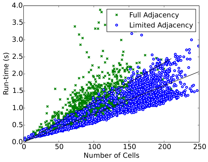
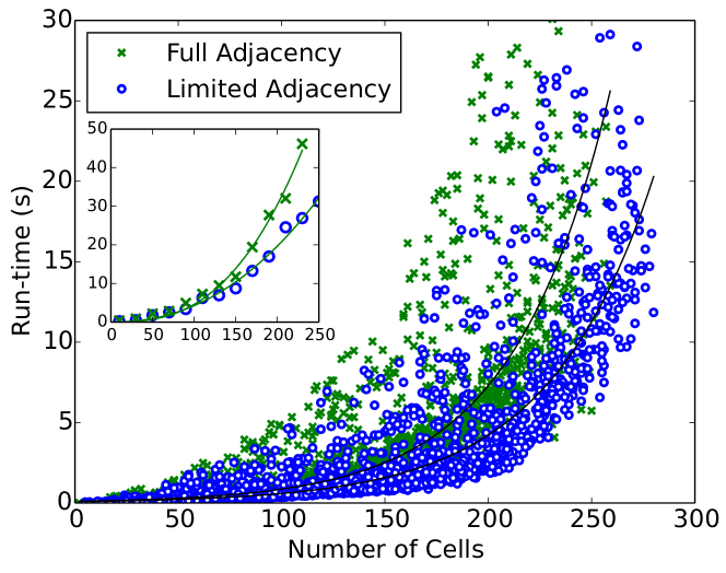
We have not yet commented on embedding run-times. For such a specific class of embedding problems, it is not meaningful to discuss theoretical worst-cases for time complexity. Instead, we consider only a best-fit to the average run-times for the generated circuits. More specifically, we quantize the algorithm run-times by the value of the fitted model at the 50% embedding probability (50P) size . Fig. 13 shows the average run-times for the generated circuits for both algorithms and both adjacency types. For the Dense Placement algorithm, the local nature of cell placement leads one to expect an approximately linear relationship between circuit size and run-time, as can be seen. For the Heuristic algorithm run-times, the best fit model was found to be exponential. Note the significant difference in time scale between the two algorithms, particularly for large circuits. The Heuristic algorithm is reported in [21] to have a worst case time complexity of with and the number of nodes and edges in the source graph, , and the target graph, . In our case is the QCA circuit connectivity graph and the Chimera graph. Depending on the complexity of a circuit of cells and the range of included interactions, the number of edges in is between and . Hence the worst case time complexity of the heuristic algorithm should be between and for a processor containing qubits. For a given processor, we should then expect the run-times to have an upper bound of the form with . The inset in Fig. 13b shows the maximum run-times within bins of 20 cells and the associated power law fits. The trends for limited and full adjacency were found to have powers of and which lie within expected values. All embeddings were done using a single core of an Intel Core i7-2670QM processor.
IV-C Scaling performance
| Method | (cells) | (ms) | ||
|---|---|---|---|---|
| DP-L | ||||
| DP-F | ||||
| Heur-L | ||||
| Heur-F |
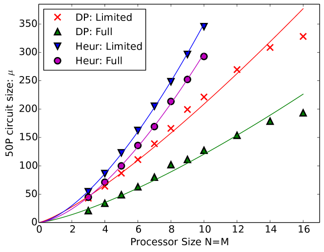
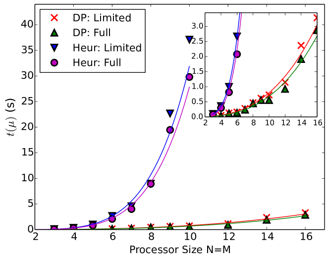
Here we investigate the trend of the 50P circuit size, , and the characteristic run-time, , of both algorithms over a range of processor sizes. We consider only square processors. That is, we assume there are rows and columns of qubit tiles. Due to its exponential run-time performance, we only tested the Heuristic algorithm up to processors of size . The Dense Placement algorithm was tested on processors up to size . The estimated values of and associated run-times are shown in Fig. 14 with power law fits. The fit parameters are included in Table III where and . The inset in Fig. 14b has the y-range expanded to better see the Dense Placement algorithm performance. While the power law fits for appear accurate up to , there is a notable fall-off for the Dense Placement algorithm for larger processor sizes, likely due to the need to coordinate the discussed long chains for the final cell placements.
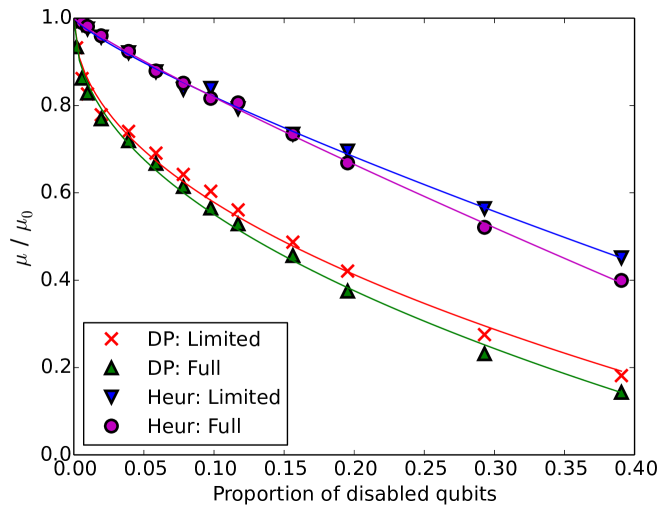
IV-D Resilience to Processor Yield
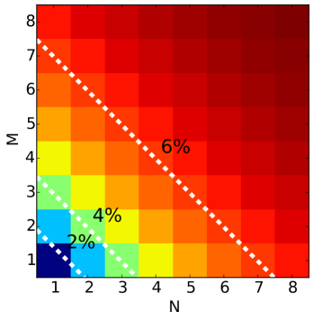
So far, we have assumed all of the qubits and couplers in the processor to be available/active. Here we investigate the performance of both algorithms for generated circuits with different percentages of the available qubits disabled. A new set of disabled qubits is uniformly generated for each embedding trial for each circuit. Fig. 15 shows the relative values for different percentages of disable qubits on a 512 qubit processor. Here indicates the value of when no qubits are disabled. We fit a model of the form
| (9) |
where is the proportion of qubits disabled. As typical values of are small (), of importance is the observation that for the Dense Placement algorithm falls off quickly with . In contrast, the Heuristic algorithm seems to be much more resilient to yield.
V Conclusion
In this paper, we have discussed the potential for applying D-Wave Systems Inc.’s current quantum annealing architecture to investigate characteristics of large QCA circuits. We have introduced two approaches to the problem of embedding QCA circuits onto D-Wave’s quantum annealing processor and characterised these approaches using benchmark and generated circuits. Estimates were made of the embeddable circuit sizes and characteristic run-times for different processor sizes, with characteristic circuit sizes defined as the size at which a single embedding attempt was 50% successful. The Dense Placement algorithm, efficient at tightly packing low connectivity nodes, required fewer qubits to embed QCA circuits when a limited set of interactions was considered. For a higher connectivity representation of QCA circuits, D-Wave’s Heuristic algorithm required fewer qubits. In all cases, the Heuristic algorithm was able to embed larger circuits than the Dense Placement algorithm. However, the local nature of the Dense Placement algorithm allowed for significantly faster run-times. It was observed that the embeddable circuit size for the Heuristic algorithm was more resilient to disabled qubits than the Dense Placement algorithm. For the the 512 qubit Vesuvius processor with no disabled qubits, we estimate characteristic circuit sizes of approximately 166 and 102 cells for limited and full adjacency for the Dense Placement algorithm and 248 and 213 cells respectively for the Heuristic algorithm with characteristic run-times for the two algorithms of approximately 0.5 and 9 seconds. For the 1152 qubit “Washington” processor, we estimate characteristic circuit sizes of 270 and 154 cells for limited and full adjacency with the Dense Placement algorithm and, extending the observed trend for the Heuristic algorithm, approximately 460 and 400 cells respectively for the Heuristic algorithm with characteristic run-times of approximately 1 and 80 seconds.
References
- [1] I. Amlani, A. O. Orlov, G. Toth, G. H. Bernstein, C. S. Lent, and G. L. Snider, “Digital logic gate using quantum-dot cellular automata,” Science, vol. 284, no. 5412, pp. 289–291, 1999.
- [2] G. Csaba, A. Imre, G. H. Bernstein, W. Porod, and V. Metlushko, “Nanocomputing by field-coupled nanomagnets,” IEEE Transactions on Nanotechnology, vol. 1, no. 4, pp. 209–213, Dec 2002.
- [3] M. Macucci, M. Gattobigio, L. Bonci, G. Iannaccone, F. Prins, C. Single, G. Wetekam, and D. Kern, “A QCA cell in silicon-on-insulator technology: theory and experiment,” Superlattices and Microstructures, vol. 34, no. 3–6, pp. 205 – 211, 2003, proceedings of the joint 6th International Conference on New Phenomena in Mesoscopic Structures and 4th International Conference on Surfaces and Interfaces of Mesoscopic Devices.
- [4] Y. Lu and C. S. Lent, “Counterion-free molecular quantum-dot cellular automata using mixed valence zwitterions - A double-dot derivative of the [closo-1-CB9H10]- cluster,” Chemical Physics Letters, vol. 582, pp. 86–89, Sep. 2013.
- [5] J. A. Christie, R. P. Forrest, S. A. Corcelli, N. A. Wasio, R. C. Quardokus, R. Brown, S. A. Kandel, Y. Lu, C. S. Lent, and K. W. Henderson, “Synthesis of a neutral mixed-valence diferrocenyl carborane for molecular quantum-dot cellular automata applications,” Angewandte Chemie International Edition, vol. 54, no. 51, pp. 15 448–15 451, 2015.
- [6] B. Tsukerblat, A. Palii, J. M. Clemente-Juan, and E. Coronado, “Mixed-valence molecular four-dot unit for quantum cellular automata: Vibronic self-trapping and cell-cell response,” The Journal of Chemical Physics, vol. 143, no. 13, p. 134307, 2015.
- [7] R. A. Wolkow, L. Livadaru, J. Pitters, M. Taucer, P. Piva, M. Salomons, M. Cloutier, and B. V. C. Martins, “Silicon atomic quantum dots enable beyond-cmos electronics,” in Field-Coupled Nanocomputing - Paradigms, Progress, and Perspectives, 2014, pp. 33–58.
- [8] C. Lent, P. D. Tougaw, W. Porod, and G. Bernstein, “Quantum cellular automata,” Nanotechnology, vol. 4, no. 1, pp. 49–57, 1993.
- [9] P. D. Tougaw and C. Lent, “Dynamic behavior of quantum cellular automata,” Journal of Applied Physics, vol. 80, no. 8, pp. 4722–4736, Oct 1996.
- [10] G. Tóth and C. S. Lent, “Role of correlation in the operation of quantum-dot cellular automata,” Journal of Applied Physics, vol. 89, no. 12, pp. 7943–7953, 2001.
- [11] K. Hennessy and C. S. Lent, “Clocking of molecular quantum-dot cellular automata,” Journal of Vacuum Science & Technology B, vol. 19, no. 5, pp. 1752–1755, 1994.
- [12] M. W. Johnson, P. Bunyk, F. Maibaum, E. Tolkacheva, A. J. Berkley, E. M. Chapple, R. Harris, J. Johansson, T. Lanting, I. Perminov, E. Ladizinsky, T. Oh, and G. Rose, “A scalable control system for a superconducting adiabatic quantum optimization processor,” Superconductor Science and Technology, vol. 23, no. 6, p. 065004, 2010.
- [13] R. Harris, M. W. Johnson, T. Lanting, A. J. Berkley, J. Johansson, P. Bunyk, E. Tolkacheva, E. Ladizinsky, N. Ladizinsky, T. Oh, F. Cioata, I. Perminov, P. Spear, C. Enderud, C. Rich, S. Uchaikin, M. C. Thom, E. M. Chapple, J. Wang, B. Wilson, M. H. S. Amin, N. Dickson, K. Karimi, B. Macready, C. J. S. Truncik, and G. Rose, “Experimental investigation of an eight-qubit unit cell in a superconducting optimization processor,” Phys. Rev. B, vol. 82, p. 024511, Jul 2010.
- [14] J. Retallick, M. Babcock, M. Aroca-Ouellette, S. McNamara, S. Wilton, A. Roy, M. Johnson, and K. Walus, “Embedding of quantum-dot cellular automata circuits onto a quantum annealing processor,” in 2014 Conference on Optoelectronic and Microelectronic Materials Devices, Dec 2014, pp. 200–203.
- [15] F. Karim and K. Walus, “Efficient simulation of correlated dynamics in quantum-dot cellular automata (QCA),” Nanotechnology, IEEE Transactions on, vol. 13, no. 2, pp. 294–307, March 2014.
- [16] N. G. Dickson, M. W. Johnson, M. H. Amin, R. Harris, F. Altomare, A. J. Berkley, P. Bunyk, J. Cai, E. M. Chapple, P. Chavez, F. Cioata, T. Cirip, P. deBuen, M. Drew-Brook, C. Enderud, S. Gildert, F. Hamze, J. P. Hilton, E. Hoskinson, K. Karimi, E. Ladizinsky, N. Ladizinsky, T. Lanting, T. Mahon, R. Neufeld, T. Oh, I. Perminov, C. Petroff, A. Przybysz, C. Rich, P. Spear, A. Tcaciuc, M. C. Thom, E. Tolkacheva, S. Uchaikin, J. Wang, A. B. Wilson, Z. Merali, and G. Rose, “Thermally assisted quantum annealing of a 16-qubit problem,” Nat Commun, vol. 4, pp. 1903+, May 2013.
- [17] P. Bunyk, E. Hoskinson, M. Johnson, E. Tolkacheva, F. Altomare, A. Berkley, R. Harris, J. Hilton, T. Lanting, A. Przybysz, and J. Whittaker, “Architectural considerations in the design of a superconducting quantum annealing processor,” Applied Superconductivity, IEEE Transactions on, vol. 24, no. 4, pp. 1–10, Aug 2014.
- [18] L. D. Landau, “Zur theorie der energieübertragung,” Phys. Z. Sowjetunion, vol. 2, pp. 46–51, 1932.
- [19] C. Zener, “Non-adiabatic crossing of energy levels,” Proceedings of the Royal Society of London A: Mathematical, Physical and Engineering Sciences, vol. 137, no. 833, pp. 696–702, 1932.
- [20] L. McMurchie and C. Ebeling, “Pathfinder: A negotiation-based performance-driven router for FPGAs,” in Field-Programmable Gate Arrays, 1995. FPGA ’95. Proceedings of the Third International ACM Symposium on, 1995, pp. 111–117.
- [21] J. Cai, W. G. Macready, and A. Roy, “A practical heuristic for finding graph minors,” ArXiv e-prints, Jun. 2014.