Adatom diffusion in high electric fields
Abstract
Strong electric fields are known to create biased adatom migration on metallic surfaces. We present a Kinetic Monte Carlo model that can simulate adatom migration on a tungsten (W) surface in electric fields. We validate our model by using it to calculate the drift velocity of the adatom at different fields and temperature and comparing the results with experimental data from the literature. We obtain excellent agreement.
I Introduction
It has been seen that surface protrusions or at least sharp surface feature can develop in strong electric fields [1, 2]. Such asperities, if large enough, may be the cause for vacuum breakdowns that occurs even in ultra high vacuum environments, as they may enhances the local field enough to cause field emission [1, 3, 4]. The bias effect of electric fields have been extensively studied both experimentally and theoretically by S. C. Wang and T. T. Tsong, who studied how W adatoms moved on flat facets of W tips in different fields with field-ion microscope [5, 6]. They were able to measure how the drift velocity of the adatoms depends on different fields. In this paper we will study the atom migration in electric fields using a Kinetic Monte Carlo (KMC) model.
II Methods
For simulating the surface diffusion of atoms, we use the KMC code Kimocs, which is described in detail in Ref. [7]. The code uses a rigid lattice, where the atom migration jumps are characterized by the number of first- and second-nearest neighbour atoms. The migration events, where an atom may jump to any unoccupied first-nearest neighbour lattice position, are chosen according to the general KMC algorithm [8, 9, 10]. The transition rates are calculated according to the Arrhenius formula
| (1) |
where s-1 is the attempt frequency, taken to be the same for all atom jump events; is the Boltzmann constant, is the temperature of the system, and is the migration energy barrier. The time increments are calculated according to the resident time algorithm [9]. In our model, the electric field above an arbitrarily rough, but still continuous, metallic surface is calculated using the field solver developed by M. Veske et al. [11], which solves Laplace’s equation
| (2) |
where is the electrostatic potential [12].
In our KMC model, the migration energy barrier of a jump is modified by the field according to T. T. Tsong and G. Kellogg’s formula [5]
| (3) |
where is the migration energy barrier in the absence of any field. On the W{110} surface, only one barrier is possible. We use the value eV [13]. is the field at the initial lattice position and is the field at the saddle point of the jump. is the surface-induced dipole moment and is the polarizability; these values may be different at equilibrium lattice points and saddle points (as indicated by the subscripts 0 and ).
III Results and discussion
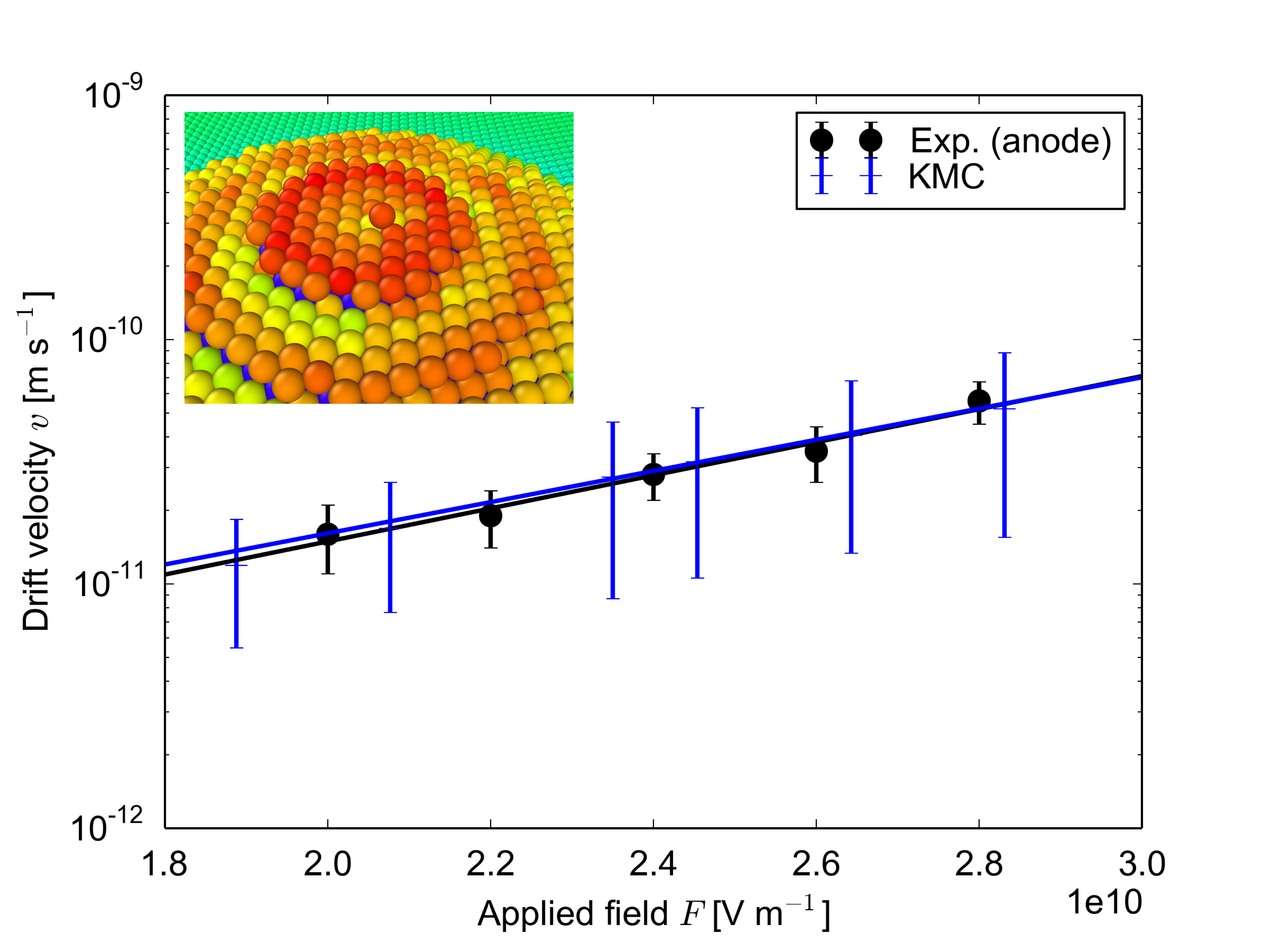
We verify the model for migration under electric fields by comparing the adatom drift velocity on W{110} surfaces under different applied electric fields and compare with the experimental data by Wang and Tsong [6]. The experimental conditions were simulated by having a 3.0 nm high hemisphere with a radius of 7.44 nm made of W atoms in a body-centred-cubic lattice on a nm2 W{110} substrate surface. The top {110} facet of the hemisphere has a diameter of 2.22 nm. For an anode field of Vm-1 at the centre of the facet, a gradient of ( Vm-2 between the centre and the facet edge is obtained, in good agreement with the values reported for the experiment (They report a gradient of V m-2 for the same central field [6]).
The average drift velocity was calculated by having an adatom migrating on the facet, starting one lattice position off the centre. After 3 KMC steps, the drift velocity was calculated by dividing the displacement by the time. This was repeated ten times for every applied field between and Vm-1. The temperature was set to 280.0 K, as in the experiment [6]. Using em ( Cm) and em2V-1 ( Cm2V-1), which were both calculated using DFT, and em, which is fitted, we obtain excellent agreement with the experimental data, as shown in Fig. 1. We are here assuming that the polarizability is the same at both the lattice position and the saddle position, i.e. .
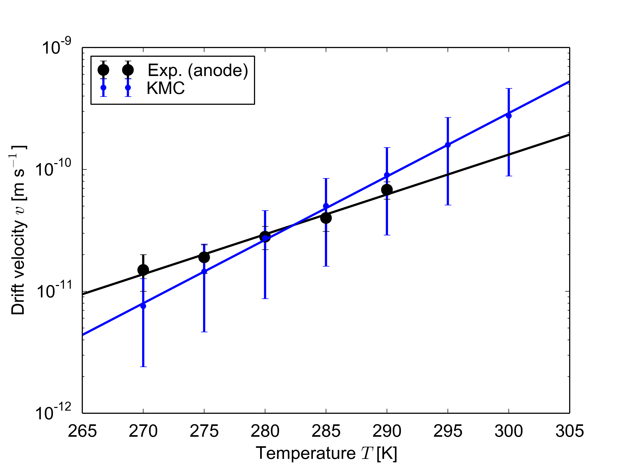
We also calculated the drift velocity at different temperatures between 270 to 290 K while keeping the applied field constant at V m-1. The results are shown in Fig. 2 and show good agreement with the experimental data [6].
IV Conclusion
We have presented a model for simulating surface diffusion of adatoms under electric fields. We have shown that our model gives excellent agreement with earlier experimental measurements of the drift velocity of W adatom diffusion on a closed-packed W{110} surface in different applied electric fields and at different temperatures.
Acknowledgement
The authors acknowledges support by Academy of Finland (Grant No. 285382 and No. 269696), CERN, and Svenska Kulturfonden (Arvid och Greta Olins Fond). Computing resources were provided by the Finnish IT Center for Science (CSC).
References
- [1] K. Nagaoka, H. Fujii, K. Matsuda, M. Komaki, Y. Murata, C. Oshima, and T. Sakurai, “Field emission spectroscopy from field-enhanced diffusion-growth nano-tips,” Applied surface science, vol. 182, no. 1, pp. 12–19, 2001.
- [2] V. T. Binh and N. Garcia, “On the electron and metallic ion emission from nanotips fabricated by field-surface-melting technique: experiments on w and au tips,” Ultramicroscopy, vol. 42, pp. 80–90, 1992.
- [3] A. Navitski, S. Lagotzky, D. Reschke, X. Singer, and G. Müller, “Field emitter activation on cleaned crystalline niobium surfaces relevant for superconducting rf technology,” Physical Review Special Topics-Accelerators and Beams, vol. 16, no. 11, p. 112001, 2013.
- [4] T. Muranaka, K. Leifer, T. Blom, and V. Ziemann, “In-situ experiments of vacuum discharge using scanning electron microscopes,” Tech. Rep., 2011.
- [5] T. Tsong and G. Kellogg, “Direct observation of the directional walk of single adatoms and the adatom polarizability,” Physical Review B, vol. 12, no. 4, p. 1343, 1975.
- [6] S. Wang and T. Tsong, “Field and temperature dependence of the directional walk of single adsorbed w atoms on the w (110) plane,” Physical Review B, vol. 26, no. 12, p. 6470, 1982.
- [7] V. Jansson, E. Baibuz, and F. Djurabekova, “Long-term stability of Cu surface nanotips,” Nanotechnology, vol. 27, no. 26, p. 265708, 2016. [Online]. Available: http://arxiv.org/abs/1508.06870
- [8] K. A. Fichthorn and W. H. Weinberg, “Theoretical foundations of dynamical monte carlo simulations,” The Journal of Chemical Physics, vol. 95, p. 1090, 1991.
- [9] A. B. Bortz, M. H. Kalos, and J. L. Lebowitz, “A new algorithm for Monte Carlo simulation of Ising spin systems,” Journal of Computational Physics, vol. 17, no. 1, pp. 10–18, 1975.
- [10] W. M. Young and E. W. Elcock, “Monte Carlo studies of vacancy migration in binary ordered alloys: I,” Proceedings of the Physical Society, vol. 89, p. 735, 1966.
- [11] M. Veske, A. Kyritsakis, F. Djurabekova, R. Aare, K. Eimre, and V. Zadin, “Atomistic modeling of metal surfaces under high electric fields: Direct coupling of electric fields to the atomistic simulations,” in Vacuum Nanoelectronics Conference (IVNC), 2016 29th International. IEEE, 2016, pp. 1–2.
- [12] J. Jackson, Classical electrodynamics. Wiley, New York, 1975.
- [13] G. Kellogg, T. Tsong, and P. Cowan, “Direct observation of surface diffusion and atomic interactions on metal surfaces,” Surface Science, vol. 70, no. 1, pp. 485–519, 1978.