Greatly enhanced light emission of MoS2 using photonic crystal heterojunction
Abstract
We study the effect of one-dimensional (1D) photonic crystal heterojunction (h-PhC) on the light absorption and light emission of monolayer molybdenum disulfide (MoS2), and obtained the analytical solution of the light absorption and emission of two-dimensional materials in 1D h-PhC. Simultaneously enhancing the light absorption and emission of the medium in multiple frequency ranges is easy as h-PhC has more models of photon localization than the common photonic crystal. Result shows that h-PhC can simultaneously enhance the light absorption and emission of MoS2 and enhance the photoluminescence spectrum of MoS2 by 2-3 orders of magnitude.
Two-dimensional (2D) transition metal dichalcogenides (TMDCs), such as MoS2 and WSe2, are direct-gap semiconductor 2D materials with excellent optical properties and are thus considered the best materials for future optoelectronic devices[1, 2, 3, 4, 5, 6, 7]. The light absorption and emission of 2D TMDCs per unit mass are much higher than that of traditional semiconductor materials. 2D TMDCs typically have a thickness of less than 1 nm, and their light absorption and emission are weak, thus limiting their application in optoelectronic devices. However, benefit from thin thickness of 2D materials, 2D TMDCs can be combined with optical microstructures, such as photonic crystals, microcavities, and surface plasmas, and then enhance their light absorption[8, 9, 10, 11, 12, 13, 14, 15, 16, 17, 18, 19, 20, 21, 22, 23, 24, 25, 26, 27, 28, 29, 30] and emission[8, 9, 31, 32, 33, 34, 35, 36, 37, 38, 39, 40] due to the optical localization in these structures. Lien et al. [8] and Serkan et al. [9]used surface plasmas or optical multilayers to enhance the light absorption and emission of MoS2 or WSe2, thus enhancing the photoluminescence (PL) of MoS2 or WSe2 by 10-30 times.
To further enhance the light emission and absorption of 2D TMDCs, we investigated the effect of photonic crystal heterojunction (h-PhC) on the light absorption and emission of MoS2. Similar to the semiconductor heterojunction, h-PhC comprises photonic crystals (PhC) with different lattice constants or shapes[41]. Earlier studies have found that h-PhC that comprise different PhCs can obtain strong light localization in several frequency ranges[41, 42]. On the basis of these findings, one can place h-PhC that are formed by different PhCs at intervals to form a multimode high-speed optical waveguide.
Thus, if 2D TMDCs are combined with h-PhC, the strong light localization of h-PhC in multiple frequency ranges can simultaneously enhance the light emission and absorption of 2D TMDCs. We therefore conducted a detailed study. h-PhC consists of 1D PhCs with two kinds of crystal lattices that form an h-PhC microcavity structure. To thoroughly understand the light absorption and emission in h-PhC, we first identified the analytical solution of the light absorption and emission of MoS2 in h-PhC. The findings indicate that h-PhC can enhance the light absorption and emission of MoS2 and enhance the PL spectrum of MoS2 by 2-3 orders of magnitude, which has a promising prospect and important application value in fluorescent probe, 2D LED, etc. The analytical solution can be used not only for the light absorption and emission in h-PhC but also for the calculation of other 1D PhC-2D materials composite structures.
Model and theory
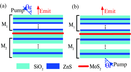
The structure of h-PhC is shown in Fig. 1, i.e., structure. and layers constitute the two distributed Bragg reflectors (DBRs) , and and are the numbers of cycles. The and layers are made of SiO2, and the refractive index [43]. , is wavelength of the input light beams, and the thicknesses of the and layers are and , respectively. and is the is the center wavelength of the the upside PhC and the bottom PhC, respectively. and layers are composed of ZnS. The refractive index [44]. The thicknesses of the and layers are and . The and layers are made of SiO2, and their thicknesses are and , respectively. The M layer is the MoS2 layer. Its thickness is 0.65 nm.
To model the absorption of MoS2 in this structure, the transfer matrix method is used first [45, 21]. In the lth layer, the electric field of the TE mode light beam with incident angle is given by
| (1) |
where is the wave vector of the incident light, is the unit vectors in the z direction, and is the position of the lth layer in the x direction. And the magnetic field of the TM mode in the lth layer is given by
| (2) |
The electric (magnetic) fields of TE (TM) mode in the (l+1)th and lth layer are related by the matrix utilizing the boundary condition
| (5) | ||||
| (6) |
where ()for TE (TM) mode, is the permeability, is the complex dielectric permittivity, and is the thickness of the lth layer. Thus, the fields in the (l+1)th layer are related to the incident fields by the transfer matrix
| (7) |
To thoroughly describe the light absorption and emission of MoS2 in h-PhC, improve the computational speed to optimize the structure, and help scholars who are not familiar with the transfer matrix method for computing, we obtained the analytical solution of the light absorption and emission of MoS2 in h-PhC using the transfer matrix method. Since the transfer matrix of the electric fields of TE mode and the transfer matrix of magnetic fields of TM mode have the same form, we only shows the analytical solution of the TE mode. First, for a N-period PhC in air, the transfer matrix can be write as[46]
| (8) |
where , is the Bloch phase in each period, and is the transmission amplitude and reflection amplitude of the each period [46]. For the upper part PhC in the h-PhC, the right hand side is not air. By multiplying the transfer matrix of PhC to the C1 layer and the inverse transfer matrix of PhC to the air layer we can get the transfer matrix of the upper part PhC
| (11) | ||||
| (14) |
where is the refractive index of C1 and C2 layers, is the propagation angle in the C1 and C2 layer. Similar, we can get the transfer matrix of the lower part PhC,
| (17) | ||||
| (20) |
where is the microcavity length, wave vector of the light in the C1 or C2 layer. Take the approximate , where wave vector of the light in the MoS2 layer and is the thickness of the and MoS2 layer, the transfer matrix of the MoS2 layer is
| (23) |
where , and . Thus, the total transfer matrix of the , , and MoS2 layer is
| (24) |
The total transfer matrix of the h-PhC is
| (25) |
we can get the matrix element
| (26) |
and
| (27) |
where , The transmittance of the h-PhC is ; the reflectance of the h-PhC is [11, 46]; the absorption of MoS2 layer .
The spontaneous emission of the monolayer MoS2 in the h-PhC can be treated as two emitted correlated wavepackets, upward (downward) propagating wave packet (). The emission wavepackets are partially transmitted and reflected by the two DBRs. The filed amplitude of the light emitted out from the exit DBR mirror is given by [47, 48, 49]
| (28) |
where and is the reflection amplitude and transmission amplitude of the exit DBR mirror, respectively, is the reflection amplitude of the back DBR mirror, is the distance between the monolayer MoS2 and back DBR mirror. When the pump and outgoing lights are on the same side of the h-PhC, , ; When the pump and outgoing lights are on the different side of the h-PhC, , ; is the electric amplitude against time for a single emission event (in either direction), is the optical length of microcavity, is the refractive index of the C1 and C2 layer. By using the Fourier transform, the emitted radiation from the top DBR mirror in the frequency domain can be written as
| (29) |
Neglected the changes of the spontaneous time, integral of Eq. (29), the emission intensity can be calculated by [47, 48]
| (30) |
where and is the transmittance and reflectance of the exit DBR mirror, respectively, and is the the transmittance and reflectance of the back DBR mirror with the MoS2 TFT, respectively.
RESULTS
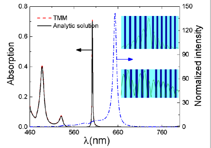
We first calculated the absorption and the relative radiation intensity of MoS2 when the pump and outgoing lights are on the same side of the h-PhC. The calculated parameters are as follows: nm, nm, nm, nm, , and . The incident angle . The pump light is in TE mode. The outgoing light is vertically emitted. Two strong absorption peaks emerge at wavelengths of 488 (consistent with the wavelength of the pump light used in the experiment[9]) and 602 nm. Quite small difference can be found between the calculation results of the analytical solution and the transfer matrix method due to the approximate is used. The optical wavelength of 602 nm is in the bandgap of the two PhCs with strong localization properties (upper illustration of Figure 1) and strong absorption. The absorption can reach 0.7 or more, which is approximately 6 times more than that without h-PhC. If the wavelength of the pump light is 488 nm, it is only in the bandgap of the bottom PhC. The localization is weak. The absorption is 0.4, which is about 3 times more than that without h-PhC. The emission efficiency is enhanced by 140 times due to the high reflectivity of the PhCs on both sides. Thus, when the pump lights are 488 and 602 nm, the PL is enhanced by approximately 420 and 840 times, respectively.
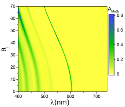
The MoS2 absorption in h-PhC is sensitive to the incidence angle. The calculation results are shown in Figure 3. The resonant wavelength of the microcavity is . is the microcavity optical path, is a positive integer, and is the propagation angle of light in the defective layer. Thus, when the incident angle increases, the resonance wavelength moves in the short-wave direction, the reflectivity of the PhCs on both sides increases, the travel path of light in MoS2 increases, and the maximum absorption can reach 0.8 or more. PL is enhanced by approximately 3 orders of magnitude.
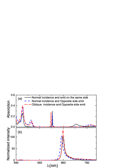
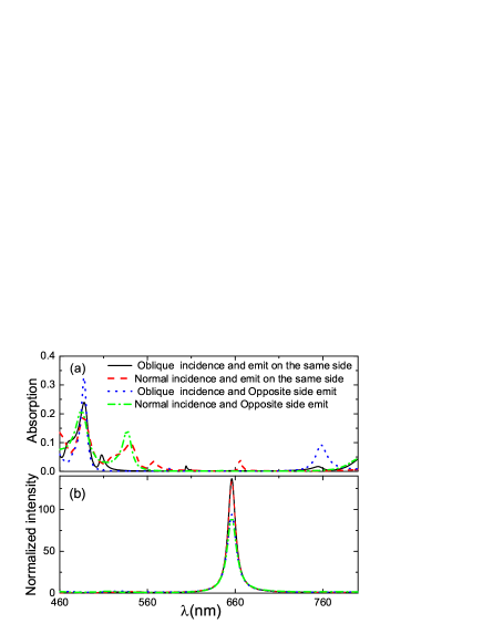
We also calculated the positive incidence of the pump light and the absorption and relative radiation intensity of MoS2 when the pump and outgoing lights are on different sides of the h-PhC. As in the experiment, in our calculation, the wavelength of the pump light is 488 nm, and the wavelength of the outgoing light approaches 660 nm. We calculated the corresponding parameters by optimizing the h-PhC structure under different pump light incidences as follows: when the pump light is normally incident and the pump and outgoing lights are on the same side of the h-PhC, nm, nm, nm, nm, , and . When the pump light is normally incident and the pump and outgoing lights are on different sides of the h-PhC, nm, nm, nm, nm, , and . When the pump light is obliquely incident and the pump and outgoing lights are on different sides of the h-PhC, nm, nm, nm, nm, , , and .
The detailed calculation results are shown in Figure 4. Regardless of whether the pump and outgoing lights are on the same or different sides of the h-PhC, the absorption of MoS2 is higher when the pump light is obliquely incident. A strong local touch in the vicinity of two wavelengths can be easily obtained as change in incidence angle can adjust the resonant wavelength. When the pump light is normally incident and the pump and outgoing lights are on different sides of the h-PhC, the absorption of MoS2 is high because if MoS2 in the microcavity structure obtains strong absorption and emission, the reflectivity of the rear reflector should be higher but the reflectivity of the front reflector should not be excessively high [18]. The bandgap width of the PhC is not big enough due to the large difference between the wavelengths of the pump and outgoing lights. The pump and outgoing lights on different sides realize this goal easily.
For comparison, we calculated the light absorption and emission of MoS2 in a homojunction. The optimized structural parameters are as follows: when the pump light is obliquely incident and the pump and outgoing lights are on the same side, nm, nm, nm, , , and . When the pump light is normally incident and the pump and outgoing lights are on the same side, nm, nm, nm, , and . When the pump light is obliquely incident and the pump and outgoing lights are on different sides, nm, nm, nm, , , and . When the pump light is normally incident and the pump and outgoing lights are on different sides: nm, nm, nm, , and . These structures show that the localization of homojunction PhC is not excessive and increasing the light absorption and emission of MoS2 at the same time is difficult. When the light emission is strong, the light absorption is usually low, with an absorption of only approximately 0.2. When the pump light is obliquely incident and the pump and outgoing lights are on different sides, the absorption is the largest (approximately 0.33) but the outgoing light enhancement is low. If light emission is enhanced using longer PhC cycles than those used in the current study, the light absorption of MoS2 will decrease. However, this case does not happen in h-PhC.
Finally, we discuss the effect of light localization and the feasibility of the experiment.
The effect of light localization: We used the Q value to judge the strength of light localization. The larger the Q value, the higher the light localization and light absorption and emission intensity of MoS2. However, the higher the Q value, the smaller the full width at half maximum of the spectral line and the narrower the absorption and PL spectra. Excessively narrow absorption and emission spectra are not conducive to practical application. Moreover, when the Q value is high, the microcavity affects the transition time of the exciton. Thus, in Optimizing the parameters, we choose and .
The feasibility of the experiment: PhC and 2D materials composite structures (particularly 2D materials-PhC microcavity) were created [14, 15, 16]. Compared with the existing structure, this structure only changes the lattice constant of the upper and lower reflectors of the PhC microcavity. Therefore, the experiment is completely achievable.
Conclusion
We studied the effect of 1D h-PhC on the light absorption and emission of monolayer MoS2 and obtained the analytical solution of light absorption and emission in 1D PhC-2D materials composite structures. h-PhC has more models of photon localization than common PhC, enhances the light emission and absorption of MoS2 simultaneously, and increases the PL spectrum of MoS2 by 2-3 orders of magnitude. When the pump light is obliquely incident and the pump and outgoing lights are on different sides of the h-PhC, it is easier to enhance the light absorption and emission of MoS2 can be enhanced at the same time. The analytical solution can be used not only for light absorption and emission in h-PhC but also for the calculation of light emission and absorption of other 1D PhC-2D materials composite structures. This study has a promising prospect and important application value in 2D material-based optoelectronic devices.
References
- [1] Wang, Q. H., Kalantar-Zadeh, K., Kis, A., Coleman, J. N. & Strano, M. S. Electronics and optoelectronics of two-dimensional transition metal dichalcogenides. Nat. Nanotech. 7, 699–712 (2012).
- [2] Congxin, X. & Jingbo, L. Recent advances in optoelectronic properties and applications of two-dimensional metal chalcogenides. Journal of Semiconductors 37, 051001 (2016). URL http://stacks.iop.org/1674-4926/37/i=5/a=051001.
- [3] Mak, K. F., Lee, C., Hone, J., Shan, J. & Heinz, T. F. Atomically thin MoS2: a new direct-gap semiconductor. Phys. Rev. Lett. 105, 136805 (2010).
- [4] Splendiani, A. et al. Emerging photoluminescence in monolayer MoS2. Nano Lett. 10, 1271–1275 (2010).
- [5] Lopez-Sanchez, O., Lembke, D., Kayci, M., Radenovic, A. & Kis, A. Ultrasensitive photodetectors based on monolayer MoS2. Nat. Nanotech. 8, 497–501 (2013).
- [6] Guo, C. F., Sun, T., Cao, F., Liu, Q. & Ren, Z. Metallic nanostructures for light trapping in energy-harvesting devices. Light: Science & Applications 3, e161 (2014).
- [7] Wang, F. et al. Progress on electronic and optoelectronic devices of 2d layered semiconducting materials. Small 1604298 (2017).
- [8] Lien, D.-H. et al. Engineering light outcoupling in 2d materials. Nano Lett. 15, 1356–1361 (2015).
- [9] Butun, S., Tongay, S. & Aydin, K. Enhanced light emission from large-area monolayer mos2 using plasmonic nanodisc arrays. Nano Lett. 15, 2700–2704 (2015).
- [10] Thongrattanasiri, S., Koppens, F. H. L. & de Abajo, F. J. G. Complete optical absorption in periodically patterned graphene. Phys. Rev. Lett. 108, 047401 (2012).
- [11] Ferreira, A., Peres, N. M. R., Ribeiro, R. M. & Stauber, T. Graphene-based photodetector with two cavities. Phys. Rev. B 85, 115438 (2012).
- [12] Ferreira, A. & Peres, N. M. R. Complete light absorption in graphene-metamaterial corrugated structures. Phys. Rev. B 86, 205401 (2012).
- [13] Wang, W. et al. Enhanced absorption in two-dimensional materials via fano-resonant photonic crystals. Appl. Phys. Lett. 106, 181104 (2015).
- [14] Furchi, M. et al. Microcavity-integrated graphene photodetector. Nano Lett. 12, 2773–2777 (2012).
- [15] Engel, M. et al. Light cmatter interaction in a microcavity-controlled graphene transistor. Nature Communications 3, 906 (2012).
- [16] Sandhu, S., Yu, Z. & Fan, S. Detailed balance analysis and enhancement of open-circuit voltage in single-nanowire solar cells. Nano Lett. 14, 1011–1015 (2014).
- [17] Zhang, Z. Z., Chang, K. & Peeters, F. M. Tuning of energy levels and optical properties of graphene quantum dots. Phys. Rev. B 77, 235411 (2008).
- [18] Vincenti, M. A., de Ceglia, D., Grande, M., D’Orazio, A. & Scalora, M. Nonlinear control of absorption in one-dimensional photonic crystal with graphene-based defect. Opt. Lett. 38, 3550–3553 (2013).
- [19] Guozhi, J., Peng, W., Yanbang, Z. & Kai, C. Localized surface plasmon enhanced photothermal conversion in bi2se3 topological insulator nanoflowers. Sci Rep. 6, 25884 (2016).
- [20] Shuyuan, X. et al. Tunable light trapping and absorption enhancement with graphene ring arrays. Phys. Chem. Chem. Phys. 18, 26661–26669 (2016).
- [21] Wu, Y.-B., Yang, W., Wang, T.-B., Deng, X.-H. & Liu, J.-T. Broadband perfect light trapping in the thinnest monolayer graphene-mos2 photovoltaic cell: the new application of spectrum-splitting structure. Scientific Reports 6, 20955 (2016).
- [22] Zheng, J., Barton, R. A. & Englund, D. Broadband coherent absorption in chirped-planar-dielectric cavities for 2d-material-based photovoltaics and photodetectors. ACS Photonics 1, 768–774 (2014).
- [23] Linshuang, L., Yue, Y., Hong, Y. & Liping, W. Optical absorption enhancement in monolayer mos2 using multi-order magnetic polaritons. Journal of Quantitative Spectroscopy and Radiative Transfer 200, 198–205 (2017).
- [24] Zhao, C. X., Xu, W., Li, L. L., Zhang, C. & Peeters, F. M. Terahertz plasmon-polariton modes in graphene driven by electric field inside a fabry-p rot cavity. Journal of Applied Physics 117, 223104 (2015).
- [25] Zu, S. et al. Active control of plasmon-exciton coupling in mos2-ag hybrid nanostructures. Advanced Optical Materials 4, 1463–1469 (2016).
- [26] Wang, M. et al. Plasmon-trion and plasmon-exciton resonance energy transfer from a single plasmonic nanoparticle to monolayer mos2. Nanoscale C7NR03909C (2017). URL http://dx.doi.org/10.1039/C7NR03909C.
- [27] Jeong, H. Y. et al. Optical gain in mos2 via coupling with nanostructured substrate: Fabry-perot interference and plasmonic excitation. ACS Nano 10, 8192–8198 (2016).
- [28] Lu, H. et al. Nearly perfect absorption of light in monolayer molybdenum disulfide supported by multilayer structures. Opt. Express 25, 21630–21636 (2017).
- [29] Yao, Z. et al. Tunable surface-plasmon-polariton-like modes based on graphene metamaterials in terahertz region. Computational Materials Science 117, 544–548 (2016).
- [30] Ansari, N. & Mohebbi, E. Increasing optical absorption in one-dimensional photonic crystals including mos2 monolayer for photovoltaics applications. Optical Materials 62, 152–158 (2016).
- [31] Wang, Z. et al. Giant photoluminescence enhancement in tungsten-diselenide-gold plasmonic hybrid structures. Nature Communications 7, 11283 (2016).
- [32] Lee, K. C. J. et al. Plasmonic gold nanorods coverage influence on enhancement of the photoluminescence of two-dimensional mos2 monolayer. Sci Rep. 5, 16374 (2015).
- [33] Sobhani, A. et al. Enhancing the photocurrent and photoluminescence of single crystal monolayer MoS2 with resonant plasmonic nanoshells. Appl. Phys. Lett. 104, 031112 (2014).
- [34] Gao, W. et al. Localized and continuous tuning of monolayer mos2 photoluminescence using a single shape-controlled ag nanoantenna. Advanced Materials 28, 701–706 (2016).
- [35] Chen, H. et al. Manipulation of photoluminescence of two-dimensional mose2 by gold nanoantennas. Sci Rep. 6, 22296 (2016).
- [36] Li, J. et al. Tuning the photo-response in monolayer mos2 by plasmonic nano-antenna. Sci Rep. 6, 23626 (2016).
- [37] Galfsky, T. et al. Broadband enhancement of spontaneous emission in two-dimensional semiconductors using photonic hypercrystals. Nano Lett. 16, 4940–4945 (2016).
- [38] Janisch, C. et al. Mos2 monolayers on nanocavities: enhancement in light-matter interaction. 2D Materials 3, 025017 (2016). URL http://stacks.iop.org/2053-1583/3/i=2/a=025017.
- [39] Zhu, Y. et al. Strongly enhanced photoluminescence in nanostructured monolayer mos2 by chemical vapor deposition. Nanotechnology 27, 135706 (2016).
- [40] Noori, Y. J. et al. Photonic crystals for enhanced light extraction from 2d materials. ACS Photonics 3, 2515–2520 (2016).
- [41] Lin, L.-L. & Li, Z.-Y. Interface states in photonic crystal heterostructures. Phys. Rev. B 63, 033310 (2001).
- [42] Zhou, Y.-S., Gu, B.-Y. & Wang, F.-H. Guide modes in photonic crystal heterostructures composed of rotating non-circular air cylinders in two-dimensional lattices. Journal of Physics: Condensed Matter 15, 4109–4118 (2003).
- [43] Palik, E. D. (ed.) Handbook of Optical Constants of Solids (Academic Press, Boston, 1985).
- [44] Klein, C. A. Room-temperature dispersion equations for cubic zinc sulfide. Appl. Opt. 25, 1873–1875 (1986).
- [45] Yariv, A. & Yeh, P. (eds.) Optical Waves in Crystals: Propagation and Control of Laser Radiation (Wiley-Interscience,, New York, 1983).
- [46] Bendickson, J. M., Dowling, J. P. & Scalora, M. Analytic expressions for the electromagnetic mode density in finite, one-dimensional, photonic band-gap structures. Phys. Rev. E 53, 4107 (1996).
- [47] Hofmann, S., Thomschke, M., Lüssem, B. & Leo, K. Top-emitting organic light-emitting diodes. Opt. Express 19, A1250 (2011).
- [48] Deppe, D. G., Lei, C., Lin, C. C. & Huffaker, D. L. Spontaneous emission from planar microstructures. Journal of Modern Optics 41, 325–344 (1994).
- [49] Yang, F.-F., Huang, Y.-L., Xiao, W.-B., Liu, J.-T. & Liu, N.-H. Control of absorption of monolayer mos2 thin-film transistor in one-dimensional defective photonic crystal. Europhysics Letters 112, 37008 (2015).
METHODS
The modified transfer matrix method is used to model the absorption of monolayer MoS2 in the photonic crystal micro-cavity.
Acknowledgements
This work was supported by the NSFC (Grant Nos. 11364033, 11764008, 61774168), Project of master’s excellent talent program in guizhou province (ZYRC[2014]008), and the Innovation Group Major Research Project of Department of Educationin in Guizhou Province (No. KY[2016]028)).
Author contributions
J.T.L. supervised the project, did the theoretical derivation and the numerical calculation, analyzed the results, and wrote the paper. T. H., W. Z. H., and W. J. B. analyzed of the results and wrote the paper. Z. Y. S. supervised the project, analyzed the results, and wrote the paper. All authors discussed the results and commented on the manuscript.
Conflict of Interest: The authors declare no competing financial interest.