New address: ] Institut für Solarenergieforschung GmbH Hameln/Emmerthal, Am Ohrberg 1, 31860 Emmerthal, Germany
Formation of a conducting LaAlO3/SrTiO3 interface studied by low energy electron reflection during growth
Abstract
The two-dimensional electron gas occurring between the band insulators SrTiO3 and LaAlO3 continues to attract considerable interest, due to the possibility of dynamic control over the carrier density, and the ensuing phenomena such as magnetism and superconductivity. The formation of this conducting interface is sensitive to the growth conditions, but despite numerous investigations, there are still questions about the details of the physics involved. In particular, not much is known about the electronic structure of the growing LaAlO3 layer at the growth temperature (around 800) in oxygen (pressure around mbar), since analysis techniques at these conditions are not readily available. We developed a pulsed laser deposition system inside a low-energy electron microscope in order to study this issue. The setup allows for layer-by-layer growth control and in-situ measurements of the angle-dependent electron reflection intensity, which can be used as a fingerprint of the electronic structure of the surface layers during growth. By using different substrate terminations and growth conditions we observe two families of reflectivity maps, which we can connect either to samples with an AlO2-rich surface and a conducting interface; or to samples with a LaO-rich surface and an insulating interface. Our observations emphasize that substrate termination and stoichiometry determine the electronic structure of the growing layer, and thereby the conductance of the interface.
pacs:
00.00, 20.00, 42.10I Introduction
Transition metal oxides, and in particular perovskites, form an important class of materials exhibiting a variety of physical phenomena such as superconductivity, magnetism and ferroelectricity. Especially interesting for possible electronics applications is the occurrence of a two-dimensional electron gas between the two band insulators LaAlO3 and SrTiO3 ohtomo04 . The emergence of this conducting interface can at least partially be explained by the so-called polar catastrophe model. In this model an increasing electrical potential builds up when charged (LaO)+ and (AlO2)- layers are alternatively stacked on top of neutral layers of SrO and TiO2. This potential is compensated by the transfer of half an electron charge from the surface to the interface. A relevant observation is that the electron gas only forms when the top LaAlO3 layer is at least four unit cells thick thiel06 . At that thickness the potential buildup is apparently enough to transfer the charge to the interface. Furthermore, the electron gas only forms at the n-type interface (TiO2/AlO2) and not at the p-type interface (SrO/LaO) ohtomo04 . At the p-type interface a structural reconstruction is energetically favored over the electronic reconstruction zhang10 .
Other observations, however, are at odds with a simple electronic reconstruction model. To name just two, electrical field build-up in the LaAlO3 layer below the critical thickness is not observed segal09 ; slooten13 , and samples grown in high oxygen partial pressure do not conduct herranz07 ; kalabu11 . Clearly, defects in the LaAlO3 layer and in the TiO2 termination layer also play an important role in the formation of the electron gas. Not surprisingly, therefore, it is very much the growth conditions which determine the conducting properties of the interface. In Pulsed laser deposition (PLD), the exact plume shape and composition as well as the oxygen pressure are of great importance, influencing the cationic stoichiometrywarusa13 ; brecken13a of the LaAlO3 film and the number of oxygen vacancies in the SrTiO3 brinkman07 . In particular, a La/Al-ratio exceeding 0.97 warusa13 was shown to fully suppress the conductivity. Similarly, high-pressure oxygen sputtering yielded a La/Al ratio well above 1 and non-conducting interfaces dildar13 . Also the occurrence of magnetism brinkman07 ; ariando11 ; dikin11 ; bert11 and superconductivity reyren07 ; joshua12 ; caviglia08 was shown to be sensitive to the oxygen pressure during growth.
Whereas differences in growth conditions are therefore known to lead to conducting or insulating samples as measured afterwards, little is known about how the electronic properties of the material develop during growth, mainly because the high temperatures and high oxygen pressure required during growth limit the abilities for in-situ analysis. For this reason we recently developed an in-situ pulsed laser deposition system inside a low-energy electron microscope. This allows us to follow the growth by monitoring oscillations in the width and intensity of the specular beam torren16 . At the same time, it allows measurements of the angle-dependent electron reflectivity of the surface with sub-unit cell precision, which yields information on the unoccupied part of the band structure jobst15 ; jobst16 . Here we show the results of the growth of LaAlO3 on SrTiO3 under different circumstances. We find clear differences in the development of the reflectivity maps when growing samples with conducting or with insulating interfaces, and relate that to the surface termination and stiochiometry of the growing film.
II Experimental setup and sample preparation
The LaAlO3/SrTiO3 interfaces are grown and studied in an aberration corrected low-energy electron microscope (LEEM) at Leiden university, called ESCHER tromp10 ; schramm11 ; schramm12 ; tromp13 . The LEEM technique has been used before to study SrTiO3 hessel14 and LaAlO3 torren15 separately. We now also developed a pulsed laser deposition (PLD) system inside the system to allow for analysis during growth, which was already used to study the growth of SrTiO3 on SrTiO3 torren16 . In order to study growth, pulsed deposition is performed alternatingly with LEEM imaging. In more detail, between every few laser / deposition pulses, the LEEM is turned on (meaning the high voltage between objective lens and sample, required for the low-energy electrons, is switched on) and diffraction images are obtained. From the diffraction images the intensity and shape of the specular diffraction spot is determined to monitor the growth. After this measurement the high voltage is turned off and deposition can continue. For growth monitoring we obtain the full-width-half-maximum (FWHM) and the peak intensity of the specular spot. In a layer-by-layer growth mode, both the FWHM and the intensity oscillate, out of phase with one another, and allow precise control over the deposition. To obtain a fingerprint of the unoccupied band structure, angle-resolved reflected electron spectroscopy (ARRES) is also performed jobst15 ; jobst16 . In this technique the electron reflection is measured depending on energy and on the in-plane wave vector which is controlled by the angle of incidence of the electron beam. ARRES utilizes the fact that the electron reflectivity strongly depends on the electron landing energy and the in-plane momentum . In particular the electron reflection is low if the material has a band at the specific (, ) of the electron so that it can couple into the band. In contrast, when (, ) of the electron coincide with a band gap the electron reflectivity is high. Hence the ”reflected-electron” or ARRES map shows a fingerprint of the unoccupied band structure. For the ARRES measurements we obtain the total (integrated) spot intensity which is independent of the surface roughness i.e. the total intensity stays constant when the surface roughens since the spot broadening lowers the maximum.
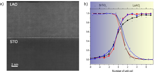
As substrates, SrTiO3 (100) single crystals from CrysTec GmbH are used which were TiO2-terminated by a buffered HF etch kawasaki94 and annealing in oxygen at 950 for one hour. The SrO-terminated substrate was prepared in a different PLD system by growing a double SrO-layer on a TiO2-terminated substrate. For the PLD targets, single crystals LaAlO3 (100) from Crystal GmbH were used. The PLD growth is performed at a pressure of mbar oxygen and if not otherwise stated at a 2 J/cm2 laser fluence with 1 Hz repetition rate. Depending on deposition speed, the deposition is briefly intermitted each 5 to 50 pulses to perform imaging and spectroscopy. This results in around 10 measurements per unit cell grown. Samples are grown at temperatures between 800 and 860 as measured with a pyrometer (emissivity 0.8). Temperature-dependent resistance measurements were performed in a Physical Properties Measurement System (PPMS, Quantum Design) in a van der Pauw configuration. In order to facilitate the discussion, samples with a conducting interface will henceforth be designated with the suffix ”C”, insulating samples will be labeled ”I”. The composition across the interface was measured by scanning transmission electron microscopy (STEM) in electron energy loss (EELS) mode on a Titan microscope operated at 300 kV. Samples were prepared by FIB milling as described elsewhere chen15 . The profiles shown below (Fig. 5b) result from the average of 5 different measurements. The integrated intensity of the Sr L-edge, Ti L edge, La M-edge and Al K -edge was normalized by dividing by the maximum. A slight cation deficiency was ignored due to the limited precision of EELS quantification. (as discussed in ref. gauq14 )
III Results
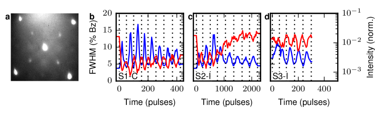
Three LaAlO3/SrTiO3 heterostructures were grown under two different growth conditions and on two kind of substrates. The first sample (S1-C) was grown with an optimal fluence of 2 J/cm2 on a TiO2-terminated SrTiO3-substrate, the second sample (S2-I) was grown with a much lower fluence by defocusing the PLD laser on the same TiO2-terminated substrate, and the third sample (S3-I) was grown with the optimal fluence of 2 J/cm2 on the SrO-terminated SrTiO3-substrate. For layer-by-layer growth control we took low-energy electron diffraction images as shown in Fig. 1a for bare SrTiO3. The starting surface shows clear diffraction spots and a 2 1 reconstruction, in line with earlier observations hessel14 . From the diffraction images, the peak intensity and full-width-half-maximum (FWHM) of the specular spot were recorded and are shown in Fig. 1b, c, d in red and blue respectively for samples S1-C, S2-I and S3-I.
Clear oscillations can be observed in both FWHM and peak intensity, which are out of phase with one another. The landing energy of the electrons (17 eV) has been optimized for maximal contrast in the oscillations. This energy is close to the out-of-phase condition where the electrons destructively interfere at the step edges on the surface. At the flat surface the coherent areas are large, resulting in sharp diffraction spots with small FWHM. When the surface roughens during growth the coherent areas become small due to the large amounts of newly grown islands, which results in low peak intensity and high FWHM. As a guide to the eye, dotted lines are plotted to indicate integer number of unit cells grown. A total of eight unit cells was grown on S1-C, S2-I and five unit cells on S3-I. Much more pulses were needed for sample S2-I (Fig. 1c) than sample S1-C and S3-I (Fig. 1b, d). From this we can conclude that the growth speed is highly reduced for the out-of-focus laser beam, as expected.
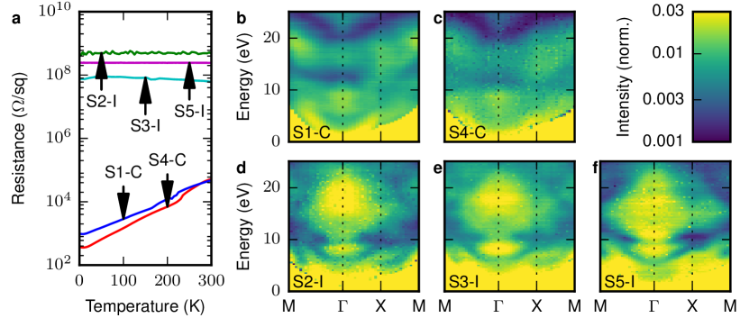
For sample S1-C (Fig. 1b) the peak intensity strongly decreases at the start to oscillate around a constant background for the remainder of the time. Sample S2-I shows the same decrease of background intensity up to two unit cells, but then comes back to the starting value between three and five unit cells. Sample S3-I does not show the decrease at the start and keeps oscillating around a constant value. This change in background intensity is related to the electronic structure of the surface layer as will become clear below. First we characterize the electrical properties of these samples. For this, the temperature dependence of the sheet resistance was measured and is shown in Fig. 2a for sample S1-C (blue), sample S2-I (green) and sample S3-I (cyan). Sample S1-C shows conducting behavior while sample S2-I and sample S3-I are insulating.
To fingerprint the difference between conducting and insulating samples at the growth temperature, we use angle-resolved reflected electron spectroscopy (ARRES) jobst15 as shown in Fig. 2b-f. ARRES maps of sample S1-C, S2-I and S3-I are shown in Fig. 2b, d and e respectively. These maps were measured directly after growth, at the growth temperature. The differences between the conducting and the non-conducting samples are large. The conducting sample S1-C (Fig. 2b) shows a band (minimum in intensity) around 14 eV at the -point and a V-shaped band at the top of the figure above 20 eV, while the insulating samples S2-I and S3-I (Fig. 2d,e) show a maximum (i.e. a band gap) between 14 and 22 eV around the -point.
In order to see whether this correlation is general, we measured two samples grown in other systems in ways which are known from literature to produce conducting and non-conducting samples. Sample S4-C was grown in a conventional PLD system with the possibility to grow under higher oxygen pressures which is known to result in conducting samples. Sample S5-I was grown by on-axis sputter deposition, known to result in insulating samples dildar13 . ARRES maps are shown in figure 2c and f for S4-C and S5-I respectively. Their (non-)conductance is confirmed by electrical measurements (Fig. 2a). During the ARRES measurements, both samples were kept at a high temperature in an oxygen pressure of mbar to remove any contaminants and prevent the surface from charging. Exact growth and measurement conditions can be found in the appendix. Comparing S1-C and S4-C we conclude the ARRES maps are similar and not sensitive to ex-situ transfer. The insulating samples S2-I, S3-I and S5-I in the bottom row of Fig. 2 are also similar, which leads us to conclude that the differences are intrinsic.
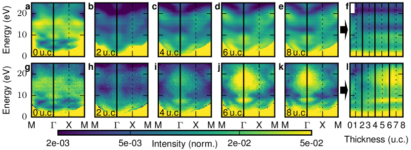
Next we consider the change of the reflectivity with thickness. Fig. 3 shows ARRES maps at the growth temperature for every second unit cell grown. Conducting sample S1-C is shown at the top (Fig. 3a-e) and insulating sample S2-I at the bottom (Fig. 3g-k). Both samples start with a TiO2-terminated SrTiO3 surface (a, g), showing the same map only slightly different in brightness. The maps show a strong change as soon as two unit cells of LaAlO3 are grown (b, h). However, the maps of the conducting sample S1-C (top, b) and insulating sample S2-I (bottom, h) still show many similarities. This changes at four unit cells of LaAlO3. While for the conducting sample S1-C (Fig. 3c) the band around at 14 eV becomes a little bit more pronounced, the non-conducting sample S2-I (Fig. 3i) strongly changes and develops a pronounced band gap around the -point for energies between 14 and 22 eV, observed as a high-intensity area. Adding more LaAlO3 up to 6 (Fig. 3d, j) and 8 (Fig. 3e, k) unit cells only leads to little changes, both for the conducting and the non-conducting samples.
To probe the changes during growth in more detail we focus on the electron reflectivity at the -point (). This is nothing else than a LEEM (or LEED) IV-curve, which is the intensity variation of a diffracted beam, in this case the specular beam, as function of electron energy. Such curves are indicated with a vertical black line in the ARRES maps in Fig. 3. These curves were taken during growth at regular intervals of 8 to 10 times per unit-cell. Results are shown in Fig. 3f and l (sample S1-C top (f) and sample S2-I bottom (l)). They show the gradual change from the SrTiO3 fingerprint to the final IV-curve of the SrTiO3/LaAlO3 heterostructure. The five solid black vertical lines between 0 and 8 u.c. correspond to the lines at the -point in the five ARRES maps on the left side of Fig. 3. The IV-curve map Fig. 3f shows that the band at 14 eV in sample S1-C appears just after two unit cells have been grown. The band around 21 eV has already appeared at this thickness. The non-conducting sample S2-I (Fig. 3l) shows both bands around two unit cells, but they vanish between three and four unit cells when the band gap appears between 14 and 22 eV. The band gap at 8 eV also clearly appears at this thickness.
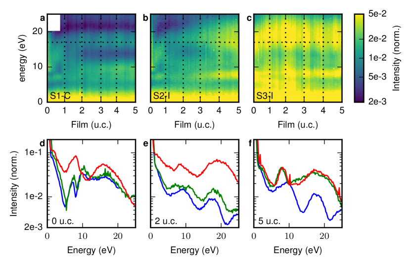
Still for samples S1-C and S2-I a zoomed-in part of the IV-curve maps for 0-5 unit cells is shown in figure 4a,b together with an IV-curve map of sample S3-I with LaAlO3 on SrO-terminated SrTiO3 (Fig. 4c), the substrate prepared in a different PLD system. For comparison, the IV-curves after deposition of 0, 2 and 5 unit cells of LaAlO3 are plotted in figure 4d,e,f. Here the IV-curves from sample S1-C are plotted in blue, sample S2-I in green and sample S3-I in red. These plots clearly show two distinct IV-curves at 0 u.c. and two distinct IV-curves after deposition of 5 u.c. of LaAlO3. The starting IV-curves at 0 u.c. correspond with the TiO2- (blue, green) and SrO-terminated (red) SrTiO3 while in the IV-curves after deposition we distinguish the conducting (blue) and non-conducting (green, red) samples. The evolution of the IV-curves during growth is different for the two insulating samples. This is very clear around 2 u.c. where sample S2-I (green) is still close to sample S1-C (blue) and not to sample S3-I (red), which is already close to the insulating final IV-fingerprint found on the non-conducting samples. As a matter of fact, the IV-curves for S3-I hardly change during growth on the SrO-terminated surface.
With these results, we can return to Figure 1, where for sample S1-C the intensity strongly decreased at the start and continued to oscillate around a low value; for sample S2-I the intensity decreased at the start, but recovered between 3 and 5 unit cells; and for sample S3-I the intensity oscillated around the starting value, and did not decrease at all. The energy of 17 eV where the data of Fig. 1 was taken is indicated with a horizontal dotted line in the IV-curve maps, Fig. 4a-c. Note that in Fig. 1 the maximum of the specular diffraction spot is plotted, which is sensitive to spot broadening due to surface roughening. This results in growth oscillations superimposed on the electron reflectivity signal. On the other hand, for Fig. 4 the intensity of the total specular spot is integrated, resulting in an intensity independent of spot shape (i.e. surface roughness) and only depending on the electron reflectivity. Combining Fig. 1 and 4 we can now conclude that the increasing background signal between 3 and 4 unit cells in Fig. 1c is caused by the appearance of the band gap (enhanced surface reflectivity) shown in Fig. 4b.
One question with respect to the out-of-focus grown sample is whether the epitaxy is impaired by the ill-defined fluence. For that we performed scanning transmission electron microscopy (STEM) experiments with high-angle annular dark-field imaging (HAADF). Samples S6-I, S7-C and S8-I were prepared in the same conditions as samples S2-I, S4-C and S3-I. For the sake of avoiding any surface influence on the compositional analysis, thick films of 20UC were grown. Figure 5a presents a typical STEM-HAADF of the LaAlO3 film on the SrTiO3 substrate. Besides a slight misorientation of the non-conducting films with respect to the substrate, good quality epitaxial growth was observed for all samples. Figure 5b shows the La- and Ti-occupancies normalized to the total A- and B-site occupancy for samples S6-I (defocused), S7-C and S8-I (SrO-terminated) in blue triangles, red squares and black circles, respectively. The A-site is represented by filled symbols, the B-site by empty symbols. A similar extent of Ti-diffusion into the LaAlO3 (4-5 unit cells) can be observed for all samples, including the out-of-focus sample S6-I. As expected, the concentration of Ti in those first unit cells of the LAO film is higher, reflecting the Al-deficiency of the growing film. On the other hand, The La/Sr intermixing is similar for samples S6-I and S7-C but Sr diffuses much further for sample S8-I (SrO-terminated), leading to a relatively lower La content. We can therefore conclude that the A-site interdiffusion is controlled by the substrate termination and not influenced by the out-of-focus condition.
IV Discussion
As mentioned in the introduction, the model of electronic reconstruction of a basically perfect interface is not enough to explain the occurrence of conductance. Questions then exist about the relative importance of the role of intermixing, oxygen vacancies, strain gradients with their ensuing buckling of the oxygen octahedra at the interface, or the stoichiometry of the LaAlO3 layer. The discussion on the La/Al-stoichiometry has started relatively recently. It has been found that the LaAlO3 film has to be Al-rich for conductance to appear warusa13 ; brecken13a , and also that the LaAlO3 stoichiometry is strongly dependent on the PLD parameters brecken12 . We will now argue that our electron reflectivity experiments precisely address the issues of stoichiometry and defects, which are crucial for the occurrence of interface conductivity. Our observations are that (i) the difference between C- and I-samples is already apparent during growth and at the growth temperature and (ii) the differences between C- and I-samples are significant on the scale of eV’s. The conclusion we draw from this is that the (electronic) structure of the LaAlO3 surface layer, which is what our experiment is most sensitive to, is different for C-samples and for I-samples. The sensitivity of the electron reflectivity to the surface layer can be demonstrated from the strong change in IV-curve seen in Fig. 4d between TiO2-terminated and SrO-terminated SrTiO3. We note that the sensitivity depends on the penetration depth, which is energy dependent. Unfortunately, calculations of the electron reflectivity or the empty band structure of different possible surfaces do not yet exist in the measured energy range. We can however sketch a scenario which can be considered for such calculations.
We start with noting that the LaAlO3 grown on TiO2-terminated SrTiO3 should be AlO2-terminated, while the LaAlO3 grown on SrO-terminated SrTiO3 should be LaO-terminated. We surmise that this difference in termination causes the strong difference between the conducting sample S1-C and the non-conducting sample S3-I. Consider now sample S2-I, which shows an IV-curve comparable to sample S1-C (AlO2-terminated) for 2 unit cells (Fig. 4e) but changes to the signature of sample S3-I (LaO-terminated) for 5 unit cells (Fig. 4f). In contrast to the other samples, sample S2-I was grown with an out-of-focus laser. From literature we know that changing the PLD parameters, in particular the fluence, changes the stoichiometry of the grown film. Furthermore, we know that Al-rich LaAlO3 results in a conducting interface and La-rich LaAlO3 in an insulating interface. From this we infer that sample S2-I, grown with an out-of-focus laser, is La-rich. In growing S2-I, growth on TiO2-terminated SrTiO3 first results in a AlO2-termination, as seen after growth of 2 unit cells. Growing further, the La-excess slowly builds up, changing the surface to LaO-rich. We note that the Ti-intermixing into the LaAlO3 found for sample S2-I could compensate the Al-deficits in the first unit cells, suppressing the effects of the La-excess in those cells. Here we should remark that DFT calculations in Ref. weiland15 showed that surfaces are not AlO2- or LaO-terminated, but rather that Al3/2O2 and La5/6O are the stable surface terminations. This implies that the AlO2 surfaces mentioned above are actually Al3/2O2 and the LaO surface are La5/6O, which does not conflict with our results. On the contrary, the fact that less La is required for the La5/6O and more Al for the Al3/2O2 surface could stimulate the transition from a Al3/2O2 to a La5/6O surface for our La-rich sample S2-I. All in all, we argue that the strong change in electron reflectivity, which is correlated to the unoccupied band structure, depends on the surface termination. From the importance of the surface for the interface conductivity as described in literature xie10 ; pentcheva12 and our findings we deduce that the excess La in the surface layer could be an essential ingredient in suppressing the electron transfer to the interface. More research has to be done to investigate the exact mechanism. Finally, we note that our La-rich and Al-rich surface signatures do not correspond with the IV-curves measured on bulk mixed ordered terminated LaAlO3 as reported before torren15 . This can however be explained by the surface reconstructions found on the bulk LaAlO3 and the difference between bulk and strained thin films.
V Summary
We have shown results of electron reflectivity experiments (ARRES) on conducting and insulating LaAlO3/SrTiO3-heterostructures during growth, at the growth temperature with sub-unit cell precision. We find distinct signatures for the conducting and non-conducting samples independent of their growth conditions. In other words, the electron reflectivity (ARRES) can predict during growth whether a sample will show conductivity.
We find that the two families of reflectivity curves (maps) can be assigned to the surface termination being either AlO2 or LaO-rich. For samples with Al-rich LaAlO3 the surface termination is directly coupled to the termination of the SrTiO3. A SrO-termination results in a LaO-rich surface, while a TiO2-termination results in an AlO2-rich surface. For the growth of La-rich LaAlO3, which we believe we achieve by out-of-focus laser growth, we find the surface termination slowly changes from AlO2-rich to LaO-rich during growth. From the importance of the surface for the interface conductivity as described in literaturexie10 ; pentcheva12 , we infer that it could be this change in surface termination that is essential in suppressing the interface conductivity for the La-rich growth.
VI Acknowledgements
We want to acknowledge Ruud Tromp, Daniel Geelen, Johannes Jobst, Regina Dittmann, Gert Jan Koster, Guus Rijnders and Jo Verbeek for discussions and advice and Ruud van Egmond and Marcel Hesselberth for technical assistance. This work was supported by the Netherlands Organization for Scientific Research (NWO) by means of an ”NWO Groot” grant and by the Leiden-Delft Consortium NanoFront. The work is part of the research programmes NWOnano and DESCO, which are financed by NWO. N.G. acknowledges funding through the GOA project “Solarpaint” of the University of Antwerp and from the FWO project G.0044.13N (Charge ordering). The microscope used in this work was partly funded by the Hercules Fund from the Flemish Government. We would also like to acknowledge networking support by the COST Action MP 1308 (COST TO-BE).
VII Appendix
Five samples have been grown for LEEM analysis. The growth parameters of these films for PLD (S1-4) and sputtering (S5) are shown in table 1 together with the temperature where the ARRES maps are measured.
| Sample Nr. | Fluence | Growth | Termination | Pressure | ARRES |
| J/cm2 | mbar | ||||
| S1-C | 2 | 780 | TiO2 | 795 | |
| S4-C | 1 | 720 | TiO2 | 1 | 630 |
| S2-I | defocus | 770 | TiO2 | 770 | |
| S3-I | 2 | 700 | SrO | 600 | |
| S5-I | n.a. | 830 | TiO2 | 3 | 560 |
References
References
- (1) A. Ohtomo and H. Y. Hwang Nature 427, 423 (2004).
- (2) S. Thiel, and G. Hammerl, and A. Schmehl, and C. W. Schneider, and J. Mannhart, Science 313, 1942 (2006).
- (3) Lixin Zhang, and Xiang-Feng Zhou, and Hui-Tian Wang, and Jing-Jun Xu, and Jingbo Li, and E. G. Wang, and Su-Hai Wei Physical Review B 82, 125412 (2010).
- (4) Y. Segal, and J. H. Ngai, and J. W. Reiner, and F. J. Walker, and C. H. Ahn, Physical Review B 80, 241107 (2009).
- (5) Slooten, E. and Zhong, Zhicheng and Molegraaf, H. J. A. and Eerkes, P. D. and de Jong, S. and Massee, F. and van Heumen, E. and Kruize, M. K. and Wenderich, S. and Kleibeuker, J. E. and Gorgoi, M. and Hilgenkamp, H. and Brinkman, A. and Huijben, M. and Rijnders, G. and Blank, D. H. A. and Koster, G. and Kelly, P. J. and Golden, M. S. Physical Review B 87, 085128 (2013).
- (6) Herranz, G. and Basletić, M. and Bibes, M. and Carrétéro, C. and Tafra, E. and Jacquet, E. and Bouzehouane, K. and Deranlot, C. and Hamzić, A. and Broto, J.-M. and Barthélémy, A. and Fert, A. Physical Review Lett. 98, 216803 (2007).
- (7) Kalabukhov, A. and Boikov, Yu A. and Serenkov, I. T. and Sakharov, V. I. and Börjesson, J. and Ljustina, N. and Olsson, E. and D. Winkler and Claeson, T. Europhys. Lett. 93, 37001 (2011).
- (8) Warusawithana, M. P. and Richter, C. and Mundy, J. A. and Roy, P. and Ludwig, J. and Paetel, S. and Heeg, T. and Pawlicki, A. A. and Kourkoutis, L. F. and Zheng, M. and Lee, M. and Mulcahy, B. and Zander, W. and Zhu, Y. and Schubert, J. and Eckstein, J. N. and Muller, D. A. and Hellberg, C. Stephen and Mannhart, J. and Schlom, D. G. Nature Comm. 4, 2351 (2013).
- (9) Breckenfeld, E. and Bronn, N. and Karthik, J. and Damodaran, A. R. and Lee, S. and Mason, N. and Martin, L. W. Physical Review Lett. 110, 196804 (2013).
- (10) Brinkman, A. and Huijben, M. and van Zalk, M. and Huijben, J. and Zeitler, U. and Maan, J. C. and van der Wiel, W. G. and Rijnders, G. and Blank, D. H. A. and Hilgenkamp, H. Nature Mat. 6, 493 (2007).
- (11) Dildar, I. M. and Boltje, D. B. and Hesselberth, M. H. S. and Aarts, J. and Xu, Q. and Zandbergen, H. W. and Harkema, S. Appl. Phys. Lett. 102, 121601 (2013).
- (12) Ariando and Wang, X. and Baskaran, G. and Liu, Z. Q. and Huijben, J. and Yi, J. B. and Annadi, A. and Barman, A. Roy and Rusydi, A. and Dhar, S. and Feng, Y. P. and Ding, J. and Hilgenkamp, H. and Venkatesan, T. Nature Comm. 2, 188 (2011).
- (13) Dikin, D. A. and Mehta, M. and Bark, C. W. and Folkman, C. M. and Eom, C. B. and Chandrasekhar, V. Phys. Rev. Lett. 107, 056802 (2011).
- (14) Bert, Julie A. and Kalisky, Beena and Bell, Christopher and Kim, Minu and Hikita, Yasuyuki and Hwang, Harold Y. and Moler, Kathryn A. Nature Physics 7, 767 (2011).
- (15) Reyren, N. and Thiel, S. and Caviglia, A. D. and Kourkoutis, L. F. and Hammerl, G. and Richter, C. and Schneider, C. W. and Kopp, T. and Ruetschi, A.-S. and Jaccard, D. and Gabay, M. and Muller, D. A. and Triscone, J.-M. and Mannhart, J. Science 317, 1196 (2007).
- (16) Joshua, Arjun and Pecker, S. and Ruhman, J. and Altman, E. and Ilani, S. Nature Comm. 3, 1129 (2012).
- (17) Caviglia, A. D. and Gariglio, S. and Reyren, N. and Jaccard, D. and Schneider, T. and Gabay, M. and Thiel, S. and Hammerl, G. and Mannhart, J. and Triscone, J.-M. Nature 456, 624 (2008).
- (18) van der Torren, A. J. H and van der Molen, S. J. and Aarts, J. Nanotechnology 27, 495702 (2016).
- (19) Jobst, J. and Kautz, J. and Geelen, D. and Tromp, R. M. and van der Molen, S. J. Nature Comm. 6, 8926 (2015).
- (20) Jobst, J. and van der Torren, A. J. H. and Krasovskii, E. E. and Balgley, J. and Dean, C. R. and Tromp, R. M. and van der Molen, S. J. Nature Comm. 7, 13621 (2016).
- (21) Tromp, R.M. and Hannon, J.B. and Ellis, A.W. and Wan, W. and Berghaus, A. and Schaff, O. Ultramicroscopy 110, 852 (2010).
- (22) Schramm, S. M. and Kautz, J. and Berghaus, A. and Schaff, O. and Tromp, R. M. and van der Molen, S. J. IBM Journal of Research and Development 55, 1 (2011).
- (23) Schramm, S. M. and Pang, A. B. and Altman, M. S. and Tromp, R. M. Ultramicroscopy 115, 88 (2012).
- (24) Tromp, R.M. and Hannon, J.B. and Wan, W. and Berghaus, A. and Schaff, O. Ultramicroscopy 127, 25 (2013).
- (25) Hesselberth, M. B. S. and van der Molen, S. J. and Aarts, J. Appl. Phys. Lett. 104, 051609 (2014).
- (26) van der Torren, A. J. H. and van der Molen, S. J. and Aarts, J. Phys. Rev. B 91, 245426 (2015).
- (27) Kawasaki, Masashi and Takahashi, Kazuhiro and Maeda, Tatsuro and Tsuchiya, Ryuta and Shinohara, Makoto and Ishiyama, Osamu and Yonezawa, Takuzo and Yoshimoto, Mamoru and Koinuma, Hideomi Science 266, 1540 (1994).
- (28) Chen, Y. Z. and Trier, F. and Wijnands, T. and Green, R. J. and Gauquelin, N. and Egoavil, R. and Christensen, D. V. and Koster, G. J. and Huijben, M. and Bovet, N. and Macke, S. and He, F. and Sutarto, R. and Andersen, N. H. and Sulpizio, J. A. and Honig, M. and Prawiroatmodjo, G. WE. D. K. and Jespersen, T. S. and Linderoth, S. and Ilani, S. and Verbeeck, J. and Van Tendeloo, G. and Rijnders, G. and Sawatzky, G. A. and Pryds, N. Nature Mat. 14, 801 (2015).
- (29) Gauquelin, N. and Benckiser, E. and Kinyanjui, M. K. and Wu, M. and Lu, Y. and Christiani, G. and Logvenov, G. and Habermeier, H.-U. and Kaiser U. and Keimer, B. and Botton G. A. Phys. Rev. B. 90 195140 (2014)
- (30) Breckenfeld, E. and Wilson, R. and Karthik, J. and Damodaran, A. R. and Cahill, D. G. and Martin, L. W. Chemistry of Materials 24, 331 (2012).
- (31) Weiland, Conan and Sterbinsky, George E. and Rumaiz, Abdul K. and Hellberg, C. Stephen and Woicik, Joseph C. and Zhu, Shaobo and Schlom, Darrell G. Phys. Rev. B 91, 165103 (2015).
- (32) Xie, Yanwu and Bell, Christopher and Yajima, Takeaki and Hikita, Yasuyuki and Hwang, Harold Y. Nano Lett. 10, 2588 (2010).
- (33) Pentcheva, R. and Arras, R. and Otte, K. and Ruiz, V. G. and Pickett, W. E. Phil. Trans. Royal Soc. A 370, 4904 (2012).