Pure Spin Current Injection in Hydrogenated Graphene Structures
Abstract
We present a theoretical study of spin-velocity injection (SVI) of a pure spin current (PSC) induced by a linearly polarized light that impinges normally on the surface of two 50% hydrogenated noncentrosymmetric two-dimensional (2D) graphene structures. The first structure, hydrogenated at only one side, labeled Up, also known as graphone, and the second, labelled Alt, is 25% hydrogenated at both sides. The hydrogenation opens an energy gap in both structures. We analyze two possibilities: in the first, the spin is fixed along a chosen direction, and the resulting SVI is calculated; in the second, we choose the SVI direction along the surface plane, and calculate the resulting spin orientation. This is done by changing the energy and polarization angle of the incoming light. The results are calculated within a full electronic band structure scheme using the Density Functional Theory (DFT) in the Local Density Approximation (LDA). The maxima of the spin-velocities are reached when eV and for the Up structure, and eV and for the Alt geometry. We find a speed of 668 Km/s and 645 Km/s for the Up and the Alt structures, respectively, when the spin points perpendicularly to the surface. Also, the response is maximized by fixing the spin-velocity direction along a high symmetry axis, obtaining a speed of 688Km/s with the spin pointing at from the surface normal, for the Up, and 906 Km/s and the spin pointing at from the surface normal, for the Alt system. These speed values are of order of magnitude larger than those of bulk semiconductors, such as CdSe and GaAs, thus making the hydrogenated graphene structures excellent candidates for spintronics applications.
pacs:
75.76+j,85.75.-d,78.67.Wj,78.90.+tI Introduction
Spintronics is an emerging research field of electronics in which the manipulation and transport of the electron spin in a solid state materials is central, adding a new degree of freedom to conventional charge manipulation.Wolf et al. (2001); Fabian et al. (2007) At present, there is an increasing interest in attaining the same level of control over the transport of spin at micro- or nano-scales, as it has been done for the flow of charge in typical 3D-bulk based electronic devices.Awschalom and Flatté (2007) Several semiconductor spintronics devices have been proposed Majumdar et al. (2006); Datta and Das (1990); Götte et al. (2016); Pershin and Di Ventra (2008), and some of them require spin polarized electrical current Awschalom et al. (2011) or pure spin current (PSC). One of the difficulties in creating measurable spin current and development of PSC based semiconductor devices is the fact that the spin relaxation time in conventional semiconducting materials cloud be too short to enable the spin transport, and may result in a non-observable spin current.Murakami et al. (2003) For PSC there is no net motion of charge; spin-up electrons move in a given direction, while spin-down electrons travel in the opposite one. This effect can be due to one-photon absorption of linearly polarized light by a semiconductor, with filled valence bands and empty conduction bands, illuminated by light with photon energy larger than the energy gap. This phenomenon can be due to spin injection,Mal’shukov et al. (2003) Hall Effects,Sinova et al. (2004) interference of two optical beams,Bhat and Sipe (2000); Najmaie et al. (2003) or one photon absorption of linearly polarized lightBhat et al. (2005). The last effect has been observed in gallium arsenide (GaAs),Zhao et al. (2006); Stevens et al. (2003) aluminum-gallium arsenide (AlGaAs),Stevens et al. (2003) and Co2FeSi.Kimura et al. (2012)
The spin velocity injection (SVI) is an optical effect that quantifies the velocity at which a PSC moves along the direction , with the spin of the electron polarized along the direction . One photon absorption of polarized light produces an even distribution of electrons in space, regardless of the symmetry of the material, resulting in a null electrical current.Bhat et al. (2005) Then, the electrons excited to the conduction bands at opposite points will result in opposite spin polarizations producing no net spin injection in centrosymmetric materials.Bhat et al. (2005) If the crystalline structure of the material is noncentrosymmetric, the spin polarization injected at a given point not necessarily vanishes.Alvarado et al. (1985); Schmiedeskamp et al. (1988) Therefore, since the velocities of electrons at opposite points are opposite, a PSC will be produced.
Graphene, an allotrope of carbon with hexagonal 2D lattice structure, demonstrates properties such as fractional quantum Hall effect at room temperature, excellent thermal transport properties, excellent conductivityHeersche et al. (2007) and strength Geim and Novoselov (2007); Reina et al. (2008); Novoselov et al. (2007); Balandin et al. (2008), being a perfect platform for two-dimensional (2D) electronic systems; however, numerous important electronic applications are disabled by the absence of a semiconducting gap. Recent studies demonstrate that a narrow band gap can be opened in graphene by applying an electric field,Zhang et al. (2009) reducing the surface area,Han et al. (2007) or applying uniaxial strain.Ni et al. (2008) Another possibility to open the gap is by doping; this has been successfully achieved using nitrogen,Wei et al. (2009) boron-nitrogen,Guo et al. (2011) silicon,Coletti et al. (2010) noble-metals,Varykhalov et al. (2010) and hydrogen.Elias et al. (2009); Guisinger et al. (2009); Samarakoon and Wang (2010) Depending on the percentage of hydrogenation and spatial arrangements of the hydrogen-carbon bonds, hydrogenated graphene demonstrates different structural configurations and a tunable electron gap, as it has been proven in Ref. Shkrebtii et al., 2012.
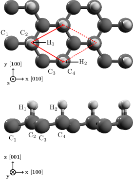
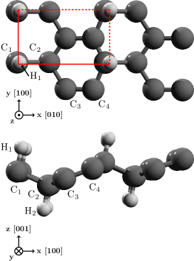
In this paper, we offer two 50% hydrogenated graphene noncentrosymmetric structures, both demonstrating a discernible band gap. The first one, labelled as the Up structure, also known as graphone,Gmitra et al. (2013) has hydrogen atoms bonded to the carbon layer only on the upper side of the structure; we consider here the magnetic isomer of graphone, with the so-called “chair” structure shown in Fig. 1. In contrast, the Alt structure, shown in Fig. 2, has hydrogen alternating on the upper and bottom sides of the carbon sheet.Zapata-Peña et al. (2016)
Both the Up and the Alt structures are noncentrosymmetric, and therefore, they are good candidates in which SVI can be induced. In this article, we address theoretically the spin-velocity injection by one-photon absorption of linearly polarized light, analyzing in our structures two possible scenarios of practical interest. The first case is by fixing the spin of the electrons along , i.e., perpendicular to the surface plane, with the resulting velocity directed along the surface of the structures on the plane. In the second case we fix the SVI velocity along the or direction, and then, the resulting spin is directed outward of the plane.
II Theory
In this section, we summarize the theoretical approach, involved in the calculation of the spin velocity injection (SVI) resulting from the pure spin current (PSC).
To calculate the velocity of the spin injection along the direction , at which the spin moves in a polarized state along direction , we start with the operator that describes the electronic SVI, written as
| (1) |
Here is the velocity operator, with being the position operator and the unperturbed ground state Hamiltonian; the Roman superscripts indicate Cartesian coordinates. To obtain the expectation value of , we use the length gauge for the perturbing Hamiltonian, written as
| (2) |
where the applied electric field of the beam of light is given by
| (3) |
In order to calculate the response of the system to , one needs to take into account the excited coherent superposition of the spin-split conduction bands inherent to the noncentrosymmetric semiconductors considered in this work. To include the coherence, we follow Ref. Nastos et al., 2007 and use a multiple scale approach that solves the equation of motion for the single particle density matrix , leading to
| (4) |
where we assumed that the conduction bands and are quasi-degenerate states, and we take at the end of the calculation. Since the spin-splitting of the valence () bands is very small, we neglect it throughout this work,Nastos et al. (2007) and then . The matrix elements of any operator are given by , where with being the energy of the electronic band and at point in the irreducible Brillouin zone (IBZ), is the Bloch state, and . Using for the expectation value of an observable , where denotes the trace, we obtain
| (5) |
where we used the closure relationship , where goes over all and states. Therefore, using Eqs. (4) and (5), the rate of change of , , is given by
| (6) |
The prime symbol ′ in the sum means that and are quasi-degenerate states, and the sum only covers these states. Replacing , in the above expression, one can show that
| (7) |
where the repeated Cartesians upperscripts are summed, and
| (8) |
is the pseudotensor that describes the rate of change of the PSC in semiconductors. To derive what we presented above we used , which follows from time-reversal invariance. Since is real, we have that . We point out that Eq. (8) is identical to Eq. (3) of Ref. Bhat et al., 2005 derived using the semiconductor optical Bloch equations. Using the closure relation,
| (9) |
We define the spin velocity injection (SVI) as
| (10) |
which gives the velocity, along direction , at which the spin moves in a polarized state along direction . The carrier injection rate is written asNastos et al. (2007)
| (11) |
where the tensor
| (12) |
is related to the imaginary part of the linear optical response tensor by .
The function allows us to quantify two very important aspects of PSC. On one hand, we can fix the spin direction along and calculate the resulting electron velocity. On the other hand, we can fix the velocity of the electron along and study the resulting direction along which the spin is polarized. To this end, the additional advantage of 2D structures, besides being noncentrosymmetric, is that we can use an incoming linearly polarized light at normal incidence, and use the direction of the polarized electric field to control . Indeed, writing , where is the polarization angle, we obtain from Eq. (10) that
| (13) |
since for the structures chosen in this article, , and . Next, we identify two options for .
II.1 Fixing the spin polarization
Analyzing the SVI, Eq. (13), we calculate the magnitude of the electron velocity along the plane of the structure, with the spin polarized along direction as
| (14) |
and define the angle at which the velocity is directed on the plane as
| (15) |
We also define two special angles
| (16) |
and
| (17) |
corresponding to the electron velocity being parallel or perpendicular to the incoming light polarization direction, respectively. The subscript denotes the spin along .
II.2 Fixing the electron velocity.
Fixing the calculated velocity along or , we define its corresponding magnitude as
| (18) |
from where we see that the spin would be oriented in the system of coordinates along the polar angle,
| (19) |
and the azimuthal angle
| (20) |
III Results
| Atom | Position (Å) | ||
|---|---|---|---|
| type | |||
| H1 | -0.615 | -1.774 | 0.731 |
| H2 | 0.615 | 0.355 | 0.731 |
| C1 | -0.615 | -1.772 | -0.491 |
| C2 | -0.615 | -0.356 | -0.723 |
| C3 | 0.615 | 0.357 | -0.490 |
| C4 | 0.615 | 1.774 | -0.731 |
| Atom | Position (Å) | ||
|---|---|---|---|
| type | |||
| H1 | -0.615 | -1.421 | 1.472 |
| C1 | -0.615 | -1.733 | 0.396 |
| C2 | 0.615 | 1.733 | 0.158 |
| C3 | 0.615 | 0.422 | -0.158 |
| C4 | -0.615 | -0.373 | -0.396 |
| H2 | -0.615 | -0.685 | -1.472 |
We present the calculated results of and for the Up and Alt structures, both noncentrosymmetric 2D carbon systems with 50% hydrogenation, which are differently structurally arranged. We remind that the Up structure has hydrogen atoms only on the upper side of the carbon sheet, while the Alt structure has alternating hydrogen atoms on the upper and bottom sides. We take the carbon lattice to be along the plane for both structures, and the carbon-hydrogen bonds are perpendicular to plane for the Up structure (Fig. 1), and off the normal for the Alt structure (Fig. 2). The coordinates for the Up and Alt unit cells of the structures are given in Tables 1 and 2, respectively.
We calculated the self-consistent ground state and the Kohn-Sham states within density functional theory in the local density approximation (DFT-LDA), with a planewave basis using the ABINIT code Gonze et al. (2009). We used Hartwigsen-Goedecker-Hutter (HGH) relativistic separable dual-space Gaussian pseudopotentials Hartwigsen et al. (1998), including the spin-orbit interaction needed to calculate from Eq. (8). The convergence parameters for the calculations, corresponding to the Up and Alt structures are cutoff energies up to 65 Ha, resulting in LDA energy band gaps of 0.084 eV and 0.718 eV, respectively, and 14452 points in the IBZ where the energy eigenvalues and matrix elements were calculated; to integrate and the linearized analytic tetrahedron method (LATM) has been used.Nastos et al. (2007) We neglect the anomalous velocity term , where is the crystal potential, in of Eq. (1), as this term is known to give small contribution to PSC.Bhat et al. (2005) Therefore, , and Eq. (1) reduces to . Finally, the prime in the sum of Eq. (8) is restricted to quasi-degenerated conduction bands and that are closer than 30 meV to each other, which is both typical laser pulse energy width and the thermal room-temperature energy level broadening.Nastos et al. (2007)
III.1 SVI: Spin velocity injection
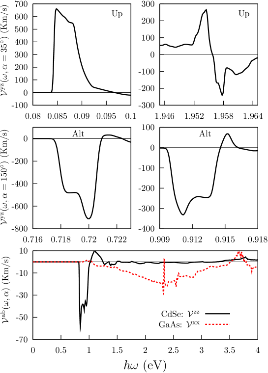
In Fig. 3, we show vs. for the velocity and spin directions and , and for the angle , at which the signal is maximized, for the Up and Alt structures, and for CdSe and GaAs bulk systems, shown for comparison. As expected from Eq. (8), starts rising from zero right at the corresponding energy gap of each system. For the 2D structures considered, the spectrum contains two narrow energy regions with strong response, while for the bulk systems, the spectra covers a rather wide energy range, but with a much weaker response. For the Up structure, at and the response is maximized, which means that an incoming light with its electric field polarized at 35∘ from the direction will induce electrons to move along (parallel to the surface), with their spin polarized along (perpendicular to the surface). Right at the energy onset, Km/s, remains almost constant for 65 meV, and then decreases to zero. A second region with high velocity is above 1.946 eV with two, opposite in sign, maxima of the speed: Km/s at eV, and Km/s at eV; a positive (negative) means that the electrons move parallel (antiparallel) to the electric field. Likewise, for the Alt structure, we also find that and maximizes the response, where two extreme values of are found, one at eV of Km/s, and the other at eV of Km/s.
For the bulk structures, we calculate from Eq. (10) by simply using . For CdSe, we find that for eV, , and Km/s, and for GaAs at eV, and Km/s, with . For these bulk semiconductors, the , , and axis are taken along the standard cubic unit cell directions, [100], [010], and [001], respectively. In Table 3, we compare for the 2D structures considered and bulk crystals. We stress that, as shown in the figure, the 2D structures have maxima in higher than for the bulk crystals by more than order of magnitude. In particular, the Alt structure demonstrates a about 12 times larger than that of CdSe and GaAs.
| Structure | System | Pol. | Energy | ||
|---|---|---|---|---|---|
| type | Ang. | [eV] | [Km/s] | ||
| Up | 2D | 35 | 0.084 | 660.5 | |
| 1.954 | 266.3 | ||||
| 1.958 | -241.4 | ||||
| Alt | 2D | 150 | 0.720 | -711.9 | |
| 0.911 | -330.6 | ||||
| CdSe | bulk | – | 0.844 | -59.0 | |
| GaAs | bulk | – | 2.324 | -28.7 | |
III.2 Fixing spin
In this subsection, we calculate , Eq. (14), for the case with the spin fixed along , i.e., directed perpendicularly to the surface of the Up and Alt structures. Also, we calculate from Eq. (15), which determines the direction of the injected electrons movement along the surface of each structure. We mention that we have also analyzed the cases when the spin is directed along or , finding similar qualitative results to those presented below.
III.2.1 Up structure
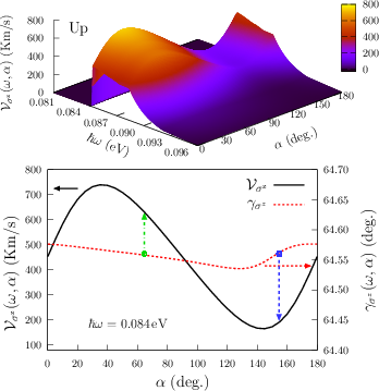
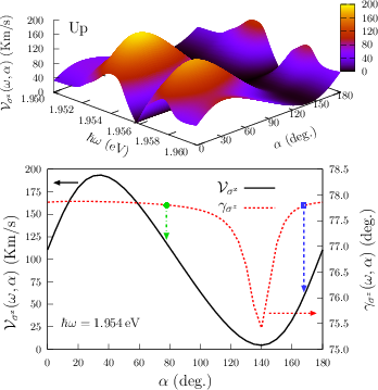
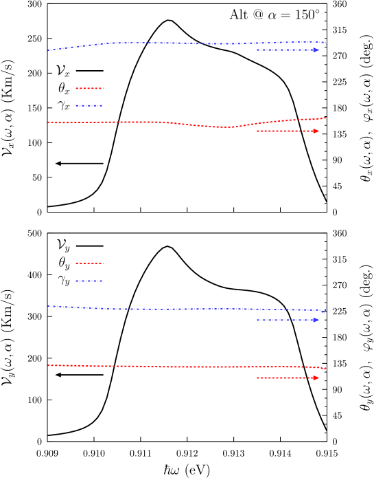
In the top panel of Fig. 4, we plot vs. 0.080 eV0.096 eV (similar energy range for the Up structure shown in the left panel of Fig. 3) and . We see a broad peak that reaches the maximum of Km/s at and eV. The variation of as a function of , which comes from the interplay of the tensor components as multiplied by the trigonometric functions of Eq. (13), gives a sizable set of values between 739.7 Km/s and 165.4 Km/s, for 0.084 eV0.090 eV. In the bottom panel, we show (left scale, black solid line) vs. , at eV, thus following the ridge in the 3D plot of the top panel. Also, we plot the corresponding velocity angle (right scale, red short-dashed line), where it is very interesting to see that is centered at 64.55∘ with a rather small deviation of only , for the whole range of . This result means that for eV and for all values of , the electrons, with the chosen spin pointing along , will move at the angle of with respect to the direction, with the range of high speeds shown in the figure. Also, from Eq. (16) we find that , with Km/s (as indicated by the green dot-dashed arrow), and that from Eq. (17), , gives , with Km/s (as indicated by the blue long-dashed arrow). Thus, at eV, an incident field, polarized at or , injects electrons with their spin polarized along , which move parallel or perpendicular to the incident electric field, with a speed of 631.14 Km/s or 191.5 Km/s, respectively.
Now, we analyze the results for the second energy range of the Up structure shown in Fig. 3. In the top panel of Fig. 5, we plot vs. 1.950 eV1.960 eV and . We see two broad peaks that maximize at and eV, with a value of Km/s, and at and eV, with a value of Km/s. We only analyze the highest maximum in the bottom panel, where we show (left scale, black solid line) vs. , at eV, thus following the highest ridge shown in the 3D plot of the top panel. Also, we plot the corresponding velocity angle (right scale, red short-dashed line), where in this case we see that the values of have more dispersion, as a function of , than for the lower energy range shown in the bottom panel of Fig. 4. However, is nearly constant from up to . In this case, we find that , with Km/s (as indicated by the green dot-dashed arrow), and that from Eq. (17), , gives , with Km/s (as indicated by the blue long-dashed arrow). Thus, through the correct choice of and we could inject electrons, in this case with their spin polarized along , which move parallel or perpendicular to the incident electric field, with sizable speeds.
III.2.2 Alt structure
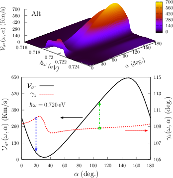
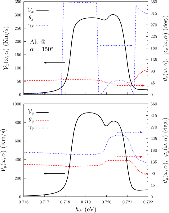
We proceed to analyze the Alt structure, just as we did with the Up structure, but in this case, we only choose the lower energy range shown in the left central panel of Fig. 3. In the top panel of Fig. 6, we plot vs. 0.715 eV0.725 eV and . We see a broad peak that maximizes at and eV, with a value of Km/s. In the bottom panel, we show (left scale, black solid line) vs. , at eV, thus following the highest ridge shown in the 3D plot of the top panel. Also, we plot the corresponding velocity angle (right scale, red short-dashed line), where now we see that is centered at having variations of for . In this case, we find that , with Km/s (as indicated by the green dot-dashed arrow), and that from Eq. (17), , gives , with Km/s (as indicated by the blue long-dashed arrow). Thus, as for the Up structure, we could inject electrons with a fixed spin, which moves parallel or perpendicular to the incident electric field.
III.3 Fixing the electron velocity
Here we calculated (Eq. (18)) after fixing the electron velocity direction, , to the or direction along the surface of the Up and Alt structures, and from Eqns. (19) and (20), we determined the corresponding polar angle, , and azimuthal angle, , of the resulting spin orientation.
III.3.1 Up structure
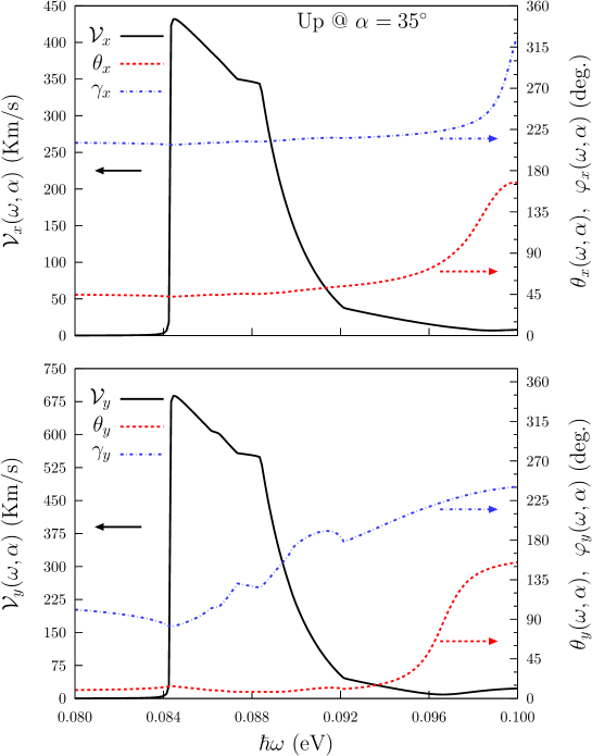
For the Up structure, we find once again that maximizes the response. In Fig. 7, we plot (left scale, black solid line), (right scale, red dashed line), and , (right scale, blue dot-dashed line), vs. , for . We see that for eV, the response has a maximum of Km/s at , and , and Km/s at , and . This means that the spin is directed upward the third quadrant of the plane when the electron moves along , and is almost parallel to the plane in the first quadrant when it moves along . Also from this figure, we see that when the electron moves along , the spin direction is almost constant for all the energies across the peak of the response, having and . When the electron moves along , the spin polar angle has again small variations, , but the azimuthal angle varies significantly, .
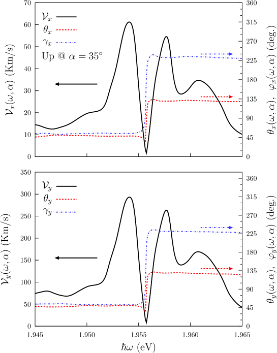
In Fig. 8, we plot vs. , in the range where there two local maxima with opposite sign at eV and eV occur. The first is the largest of the two, with Km/s, , and , for the electron moving along ; and Km/s, , and for the electron moving along . For the peak at eV, we obtain and , with Km/s and ; and , with Km/s. We remark that these angles are almost constant for all the energy values across the peak of these two local maxima, for which the spin is directed upward in the first quadrant of the plane when the electron moves along either or directions.
III.3.2 Alt structure
In Figs. 9 and 10, we plot (left scale, black solid line), (right scale, red dashed line), and , (right scale, blue dot-dashed line), vs. in two different ranges, and for . In this case, maximizes both and , as a function of . In Fig. 9, the absolute maximum Km/s is at eV, and , and Km/s at and . Thus, the spin is directed upward the fourth quadrant of the plane when the spin velocity is directed along , while it is directed downward the second quadrant when the spin velocity is directed along . Finally, in Fig. 10, the absolute maximum is at eV at Km/s, , and , and Km/s at , and , implying that the spin is directed downward the fourth quadrant of the plane when the spin velocity is directed along , while is directed downward the third quadrant when the spin velocity is directed along .
IV Conclusions
We reported the results of an ab initio calculations for the spin velocity injection (SVI) due to the one-photon absorption of the linearly polarized light in the Up and Alt 2D 50% hydrogenated graphene structures. Different possible arrangements of the of the spin injection have been considered: we made the calculations for the cases when the spin is polarized in direction or when the velocity is directed along or . To the best of our knowledge, this effect has not been previously reported in these 2D partially hydrogenated structures. We have shown that the SVI demonstrates an anisotropic behavior, which is very sensitive to the symmetry of the structures of interest. We have found that the Up structure shows the strongest response for the spin directed along , resulting in the velocity Km/s for the incoming photon energy of 0.084 eV. Also, the Alt structure has the strongest response when the spin moves along direction, resulting in Km/s for the incoming photon energy of 0.720 eV. The speed values obtained here are of the same order of magnitude as those of Ref. Najmaie et al., 2003 in unbiased semiconductor quantum well structures, while they are of order of magnitude higher compared to 3D bulk materials. Considering the fact that the spin relaxation time in pure and doped graphene ranges from nanoseconds to milliseconds, Wojtaszek et al. (2013); Ertler et al. (2009), and in view of the high spin velocity transport that we obtained for both structures, this time is sufficiently long enough to have the SVI effect observed experimentally. Therefore, the Up and the Alt graphene structures considered here are excellent candidates for the development of spintronics devices that require pure spin current (PSC).
V Acknowledgment
This work has been supported by Consejo Nacional de Ciencia y Tecnología (CONACyT), México, Grant No. 153930. R.Z.P. thanks CONACyT for scholarship support. A.I.S thanks to Centro de Investigaciones en Optica (CIO) for the hospitality during his sabbatical research leave.
References
- Wolf et al. (2001) S. A. Wolf, D. D. Awschalom, R. A. Buhrman, J. M. Daughton, S. Von Molnar, M. L. Roukes, A. Y. Chtchelkanova, and D. M. Treger, Science 294, 1488 (2001).
- Fabian et al. (2007) J. Fabian, A. Matos-Abiague, C. Ertler, P. Stano, and I. Zutic, Ac. Phys. Slov. 57, 565 (2007).
- Awschalom and Flatté (2007) D. D. Awschalom and M. E. Flatté, Nat. Phys. 3, 153 (2007).
- Majumdar et al. (2006) S. Majumdar, R. Laiho, P. Laukkanen, I. J. Väyrynen, H. S. Majumdar, and R. Österbacka, App. Phys. Lett. 89, 122114 (2006).
- Datta and Das (1990) S. Datta and B. Das, App. Phys. Lett. 56, 665 (1990).
- Götte et al. (2016) M. Götte, M. Joppe, and T. Dahm, Scientific Reports 6, 36070 (2016).
- Pershin and Di Ventra (2008) Y. V. Pershin and M. Di Ventra, Phys. Rev. B 78, 113309 (2008).
- Awschalom et al. (2011) D. D. Awschalom, D. Loss, and N. Samarth, Semiconductor Spintronics and Quantum Computation (Springer, Berlin; London, 2011).
- Murakami et al. (2003) S. Murakami, N. Nagaosa, and S. C. Zhang, Science 301, 1348 (2003).
- Mal’shukov et al. (2003) A. Mal’shukov, C. Tang, C. Chu, and K.-A. Chao, Phys. Rev. B 68, 233307 (2003).
- Sinova et al. (2004) J. Sinova, D. Culcer, Q. Niu, N. A. Sinitsyn, T. Jungwirth, and A. H. MacDonald, Phys. Rev. Lett. 92, 126603 (2004).
- Bhat and Sipe (2000) R. D. R. Bhat and J. E. Sipe, Phys. Rev. Lett. 85, 5432 (2000).
- Najmaie et al. (2003) A. Najmaie, R. D. R. Bhat, and J. E. Sipe, Phys. Rev. B 68, 165348 (2003).
- Bhat et al. (2005) R. D. R. Bhat, F. Nastos, A. Najmaie, and J. E. Sipe, Phys. Rev. Lett. 94, 096603 (2005).
- Zhao et al. (2006) H. Zhao, E. J. Loren, H. M. Van Driel, and A. L. Smirl, Phys. Rev. lett. 96, 246601 (2006).
- Stevens et al. (2003) M. J. Stevens, A. L. Smirl, R. D. R. Bhat, A. Najmaie, J. E. Sipe, and H. M. Van Driel, Phys. Rev. Lett. 90, 136603 (2003).
- Kimura et al. (2012) T. Kimura, N. Hashimoto, S. Yamada, M. Miyao, and K. Hamaya, NPG Asia Mat. 4, e9 (2012).
- Alvarado et al. (1985) S. F. Alvarado, H. Riechert, and N. E. Christensen, Phys. Rev. Lett. 55, 2716 (1985).
- Schmiedeskamp et al. (1988) B. Schmiedeskamp, B. Vogt, and U. Heinzmann, Phys. Rev. Lett. 60, 651 (1988).
- Heersche et al. (2007) H. B. Heersche, P. Jarillo-Herrero, J. B. Oostinga, L. M. K. Vandersypen, and A. F. Morpurgo, Nature 446, 56 (2007).
- Geim and Novoselov (2007) A. Geim and K. Novoselov, Nat. Mater. 6, 183 (2007).
- Reina et al. (2008) A. Reina, X. Jia, J. Ho, D. Nezich, H. Son, V. Bulovic, M. Dresselhaus, and J. Kong, Nano Lett. 9, 30 (2008).
- Novoselov et al. (2007) K. S. Novoselov, Z. Jiang, Y. Zhang, S. V. Morozov, H. L. Stormer, U. Zeitler, J. C. Maan, G. S. Boebinger, P. Kim, and A. K. Geim, Science 315, 1379 (2007).
- Balandin et al. (2008) A. Balandin, S. Ghosh, W. Bao, I. Calizo, D. Teweldebrhan, F. Miao, and C. Lau, Nano Lett. 8, 902 (2008).
- Zhang et al. (2009) Y. Zhang, T. Tang, C. Girit, Z. Hao, M. Martin, A. Zettl, M. Crommie, Y. Shen, and F. Wang, Nature 459, 820 (2009).
- Han et al. (2007) M. Han, B. Özyilmaz, Y. Zhang, and P. Kim, Phys. Rev. Lett. 98, 206805 (2007).
- Ni et al. (2008) Z. Ni, T. Yu, Y. Lu, Y. Wang, Y. P. Feng, and Z. Shen, ACS Nano 2, 2301 (2008).
- Wei et al. (2009) D. Wei, Y. Liu, Y. Wang, H. Zhang, L. Huang, and G. Yu, Nano lett. 9, 1752 (2009).
- Guo et al. (2011) B. Guo, L. Fang, B. Zhang, and J. R. Gong, Ins. J. 1, 80 (2011).
- Coletti et al. (2010) C. Coletti, C. Riedl, D. S. Lee, B. Krauss, L. Patthey, K. von Klitzing, J. H. Smet, and U. Starke, Phys. Rev. B 81, 235401 (2010).
- Varykhalov et al. (2010) A. Varykhalov, M. R. Scholz, T. K. Kim, and O. Rader, Phys. Rev. B 82, 121101 (2010).
- Elias et al. (2009) D. C. Elias, R. R. Nair, T. M. G. Mohiuddin, S. V. Morozov, P. Blake, M. P. Halsall, A. C. Ferrari, D. W. Boukhvalov, M. I. Katsnelson, A. K. Geim, et al., Science 323, 610 (2009).
- Guisinger et al. (2009) N. P. Guisinger, G. M. Rutter, J. N. Crain, P. N. First, and J. A. Stroscio, Nano Lett. 9, 1462 (2009).
- Samarakoon and Wang (2010) D. K. Samarakoon and X. Q. Wang, ACS Nano 4, 4126 (2010).
- Shkrebtii et al. (2012) A. I. Shkrebtii, E. Heritage, P. McNelles, J. L. Cabellos, and B. S. Mendoza, Phys. Stat. Sol. (c) 9, 1378 (2012).
- Gmitra et al. (2013) M. Gmitra, D. Kochan, and J. Fabian, Phys. Rev. Lett. 110, 246602 (2013).
- Zapata-Peña et al. (2016) R. Zapata-Peña, S. M. Anderson, B. S. Mendoza, and A. I. Shkrebtii, Phys. Stat. Sol. (b) 253, 226 (2016).
- Nastos et al. (2007) F. Nastos, J. Rioux, M. Strimas-Mackey, B. S. Mendoza, and J. E. Sipe, Phys. Rev. B 76, 205113 (2007).
- Gonze et al. (2009) X. Gonze, B. Amadon, P. M. Anglade, J. M. Beuken, F. Bottin, P. Boulanger, F. Bruneval, D. Caliste, R. Caracas, M. Côté, et al., Comput. Phys. Commun. 180, 2582 (2009).
- Hartwigsen et al. (1998) C. Hartwigsen, S. Goedecker, and J. Hutter, Phys. Rev. B 58, 3641 (1998).
- Wojtaszek et al. (2013) M. Wojtaszek, I. J. Vera-Marun, T. Maassen, and B. J. van Wees, Phys. Rev. B 87, 081402 (2013).
- Ertler et al. (2009) C. Ertler, S. Konschuh, M. Gmitra, and J. Fabian, Phys. Rev. B 80, 041405 (2009).