Tunable ultra-high-efficiency light absorption of monolayer graphene using critical coupling with guided resonance
Xiaoyun Jiang, Tao Wang,* Shuyuan Xiao, Xicheng Yan, and Le Cheng
Wuhan National Laboratory for Optoelectronics, Huazhong University of Science and Technology, Wuhan 430074, People’s Republic of China.
*wangtao@hust.edu.cn
Abstract
We numerically demonstrate a novel monolayer graphene-based perfect absorption multi-layer photonic structure by the mechanism of critical coupling with guided resonance, in which the absorption of graphene can significantly close to at telecommunication wavelengths. The highly efficient absorption and spectral selectivity can be obtained with designing structural parameters in the near infrared ranges. Compared to previous works, we achieve the complete absorption of single-atomic-layer graphene in the perfect absorber for the first time, which not only opens up new methods of enhancing the light-graphene interaction, but also makes for practical applications in high-performance optoelectronic devices, such as modulators and sensors.
OCIS codes: (310.6860) Thin films, optical properties; (300.1030) Absorption; (310.4165) Multilayer design.
References and links
- [1] K. S. Novoselov, A. K. Geim, S. V. Morozov, D. Jiang, Y. Zhang, S. V. Dubonos, I. V. Grigorieva, and A. A. Firsov, "Electric field effect in atomically thin carbon films," Science 306(5696), 666–669 (2004).
- [2] Chang-Hua Liu, You-Chia Chang, Theodore B. Norris, and Zhaohui Zhong, "Graphene photodetectors with ultra-broadband and high responsivity at room temperature." Nature nanotechnology 9(4), 273–278 (2014).
- [3] Shichao Song, Qin Chen, Lin Jin, and Fuhe Sun, "Great light absorption enhancement in a graphene photodetector integrated with a metamaterial perfect absorber." Nanoscale 5(20), 9615–9619 (2013).
- [4] Jianfa Zhang, Zhihong Zhu, Wei Liu, Xiaodong Yuan, and Shiqiao Qin, "Towards photodetection with high efficiency and tunable spectral selectivity: graphene plasmonics for light trapping and absorption engineering." Nanoscale 7(32), 13530–13536 (2015).
- [5] Shuyuan Xiao, Tao Wang, Yuebo Liu, Chen Xu, Xu Han, and Xicheng Yan, "Tunable light trapping and absorption enhancement with graphene ring arrays." Physical Chemistry Chemical Physics 18(38), 26661–26669 (2016).
- [6] Daniel Rodrigo, Odeta Limaj, Davide Janner, Dordaneh Etezadi, F. Javier Garcia de Abajo, Valerio Pruneri, and Hatice Altug, "Mid-infrared plasmonic biosensing with graphene." Science 349(6244), 165–168 (2015).
- [7] M. Grande, M. A. Vincenti, T. Stomeo, G. V. Bianco, D. de Ceglia, N. Aközbek, V. Petruzzelli, G. Bruno, M. De Vittorio, M. Scalora, and A. D’Orazio, "Graphene-based absorber exploiting guided mode resonances in one-dimensional gratings." Opt. Express 22(25), 31511–31519 (2014).
- [8] Quan Li, Longqing Cong, Ranjan Singh, Ningning Xu, Wei Cao, Xueqian Zhang, Zhen Tian, Liangliang Du, Jiaguang Han, and Weili Zhang, "Monolayer graphene sensing enabled by the strong Fano-resonant metasurface." Nanoscale 8(39), 17278–17284 (2016).
- [9] Shuyuan Xiao, Tao Wang, Xiaoyun Jiang, Xicheng Yan, Le Cheng, Boyun Wang, and Chen Xu, "Strong interaction between graphene layer and Fano resonance in terahertz metamaterials." Journal of Physics D: Applied Physics 50(19), 195101 (2017).
- [10] Ming Liu, Xiaobo Yin, Erick Ulin-Avila, Baisong Geng, Thomas Zentgraf, Long Ju, Feng Wang, and Xiang Zhang, "A graphene-based broadband optical modulator." Nature 474(7349), 64 (2011).
- [11] Qiaoliang Bao, and Kian Ping Loh, "Graphene photonics, plasmonics, and broadband optoelectronic devices." ACS nano 6(5), 3677–3694 (2012).
- [12] Xiaoyong He, "Tunable terahertz graphene metamaterials." Carbon 82, 229–237 (2015).
- [13] Xiaoyong He, Zhen-Yu Zhao, and Wangzhou Shi, "Graphene-supported tunable near-IR metamaterials." Opt. Lett. 40(2), 178–181 (2015).
- [14] Xiaolei Zhao, Cai Yuan, Lin Zhu, and Jianquan Yao, "Graphene-based tunable terahertz plasmon-induced transparency metamaterial." Nanoscale 8(33), 15273–15280 (2016).
- [15] Rahul Raveendran Nair, Peter Blake, Alexander N. Grigorenko, Konstantin S. Novoselov, Tim J. Booth, Tobias Stauber, Nuno MR Peres, and Andre K. Geim, "Fine structure constant defines visual transparency of graphene." Science 320(5881), 1308–1308 (2008).
- [16] Xuetao Gan, Ren-Jye Shiue, Yuanda Gao, Inanc Meric, Tony F. Heinz, Kenneth Shepard, James Hone, Solomon Assefa, and Dirk Englund, "Chip-integrated ultrafast graphene photodetector with high responsivity." Nature Photonics 7(11), 883–887 (2013).
- [17] Ren-Jye Shiue, Xuetao Gan, Yuanda Gao, Luozhou Li, Xinwen Yao, Attila Szep, Dennis Walker Jr, James Hone, and Dirk Englund, "Enhanced photodetection in graphene-integrated photonic crystal cavity." Appl. Phys. Lett. 103(24), 241109 (2013).
- [18] Hua Lu, Benjamin P. Cumming, and Min Gu, "Highly efficient plasmonic enhancement of graphene absorption at telecommunication wavelengths." Opt. Lett. 40(15), 3647–3650 (2015).
- [19] Hua Lu, Xuetao Gan, Baohua Jia, Dong Mao, and Jianlin Zhao, "Tunable high-efficiency light absorption of monolayer graphene via Tamm plasmon polaritons." Opt. Lett. 41(20), 4743–4746 (2016).
- [20] M. Grande, M. A. Vincenti, T. Stomeo, G. V. Bianco, D. de Ceglia, N. Aközbek, V. Petruzzelli, G. Bruno, M. De Vittorio, M. Scalora, and A. D’Orazio, "Graphene-based perfect optical absorbers harnessing guided mode resonances." Opt. Express 23(16), 21032–21042 (2015).
- [21] C. C. Guo, Z. H. Zhu, X. D. Yuan, W. M. Ye, K. Liu, J. F. Zhang, W. Xu, and S. Q. Qin, "Experimental Demonstration of Total Absorption over in the Near Infrared for Monolayer-Graphene-Based Subwavelength Structures." Advanced Optical Materials 4(12), 1955–1960 (2016).
- [22] C. Angulo Barrios, V. R. Almeida, R. R. Panepucci, B. S. Schmidt, and M. Lipson, "Compact silicon tunable Fabry-Perot resonator with low power consumption." IEEE Photonics Technology Letters 16(2), 506–508 (2004).
- [23] Y. S. Fan, C. C. Guo, Z. H. Zhu, W. Xu, F. Wu, X. D. Yuan, and S. Q. Qin, "Monolayer-graphene-based perfect absorption structures in the near infrared." Opt. Express 25(12), 13079–13086 (2017).
- [24] Jessica R. Piper, and Shanhui Fan, "Total absorption in a graphene monolayer in the optical regime by critical coupling with a photonic crystal guided resonance." ACS Photonics1(4), 347–353 (2014).
- [25] Ji Won Suk, Alexander Kitt, Carl W. Magnuson, Yufeng Hao, Samir Ahmed, Jinho An, Anna K. Swan, Bennett B. Goldberg, and Rodney S. Ruoff, "Transfer of CVD-grown monolayer graphene onto arbitrary substrates." ACS nano 5(9), 6916–6924 (2011).
- [26] M. A. Duguay, Y. Kokubun, Thomas L. Koch, and Loren Pfeiffer, "Antiresonant reflecting optical waveguides in SiO2-Si multilayer structures.” Appl. Phys. Lett. 49(1), 13–15 (1986).
- [27] Yurui Qu, Qiang Li, Hanmo Gong, Kaikai Du, Songang Bai, Ding Zhao, Hui Ye, and Min Qiu, "Spatially and spectrally resolved narrowband optical absorber based on 2D grating nanostructures on metallic films." Advanced Optical Materials 4(3), 480–486 (2016).
1 Introduction
Graphene, a novel two-dimensional material, has attracted particular attention recently due to its exceptional optical and electronic properties[1]. The ultra-broad spectral response, the ultra-thin atomic layer thickness and the ultra-high carrier mobility of graphene make it an ideal material for optoelectronic devices such as photodetectors[2, 3, 4, 5], biosensors[6, 7, 8, 9], and modulators[10, 11, 12, 13, 14]. However, for monolayer graphene, there are two inherent defects that hinder its high-performance on optical devices. First, the absorption of monolayer graphene is only in the visible to near-infrared ranges, which limits the quantum efficiency and results in low photoresponsivity[15]. Second, monolayer graphene does not display spectral selectivity because of its ultra-wide absorption spectrum range from the ultraviolet to the terahertz. Over the past few years, various photonic technologies have been presented to improve the absorption of the monolayer graphene by enhancing the light-graphene interaction. On the one hand, in the visible and near-infrared, one can place monolayer graphene inside various nano- or micro-cavities to achieve the perfect absorption of graphene but the devices are quite complex[16, 17]. On the other hand, Tamm plasmon polaritons (TPPs) and localized plasmons of metallic nanostructures have been used for light trapping to enhance the absorption of the monolayer graphene at communication wavelengths[18, 19]. However, the metal attenuation and surface reflection lead to a failure to achieve total absorption in monolayer graphene. Therefore, the perfect absorption of the monolayer-graphene is still rare and in urgent need for graphene functional design, especially in the visible and near infrared bands.
In this work, we theoretically investigate a graphene-based perfect absorption structure by using critical coupling with guided resonance theory, in which the absorption of monolayer graphene can reach almost at telecommunication wavelengths. These results originate from the electric field distributions surrounding monolayer graphene can be significantly enhanced by coupling mode with guided resonance of lossless multilayer dielectric combinations. Compared to the previous devices with a metallic reflector, we choice a dielectric Bragg mirrors with fewer layers as back reflector, because the metal parasitic absorption and its own attenuation reduce the light absorption of graphene[20, 21]. In addition, the proposed structure is simple and ultra-high-efficiency light absorption of graphene can be achieved by the mechanism of critical coupling. Meanwhile, the selectivity of the spectrum also can be obtained by adjusting the parameters of the structure.
2 The geometric structure and numerical model
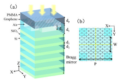
The schematic image of perfect absorption system with monolayer graphene is shown in Fig.1, a monolayer graphene is sandwiched between a D polynethy -methacrylate (PMMA) layer and a silicon dioxide (SiO2) layer with an array of cross-shaped groove air waveguide, and a dielectric Bragg mirror with -pair alternately stacked silicon ( Si) and SiO2 layers is deposited at the back side of SiO2 layer to prevent the transmission of the incident light[22]. Numerical simulations are analyzed by utilizing the finite-difference time-domain (FDTD) method. In the simulation, the monolayer graphene with a thin thickness of nm can be viewed as a conductive surface with a light conductivity of , which corresponds to free standing graphene absorbs of the incident light at the same wavelength[23]. The refractive indices of PMMA, air, SiO2 and Si are taken to be , , and , respectively. The relative geometrical parameters are labeled on Fig.1.
3 Results and discussions
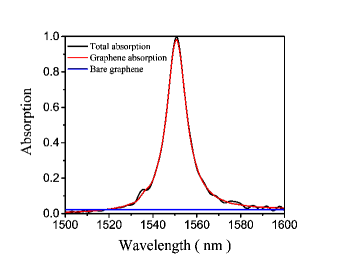
First of all, in the FDTD simulations, the normal incidence light is supposed to be TM-polarized ( the electric field parallel to the -axis ). Fig. 2 shows that the absorption of the entire structure and monolayer graphene are compared to that of bare graphene in air, when the parameters are assumed as nm, nm, nm, nm, nm, nm and nm. We set pairs as the dielectric layers in the Bragg mirror in order to make the system more stable and efficient. As depicted in Fig.2, it can be seen that the incident light is almost completely absorbed by the entire device (black line) and monolayer graphene with being inserted in the structure (red line) at resonance wavelength (at communication wavelength of nm), compared to the absorption of bare graphene (blue line) standing in air (about of the incident light) at the same band. As can be seen from the diagram, the red line and the black line are almost coincident, which indicates that the incident light is totally absorbed by the graphene in the structure. In order to account for this phenomenon, we will use the coupled mode theory with guided resonance formalism. The coupling mode theory is used to explain the input and output performance of a resonator, which affects coherence directly and indirectly. Since we chose subwavelength structure, only the zero-order mode will propagate, indicating that the incident light will excite a guided resonance at normal incidence, which corresponds to only one absorption peak in Fig.2. We consider a resonator with a single resonance at , whose input and output waves of amplitudes are and , respectively. The external leakage rate of the resonant cavity is , and the intrinsic loss rate of monolayer graphene is , the reflectivity coefficient of the system can be calculated by the equation[24],
| (1) |
and the absorption can be defined by the equation,
| (2) |
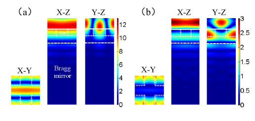
From eq and eq, it can be seen that when the system is in the resonance state (), and the external leakage rate is equal to the intrinsic loss rate of graphene (), the whole system satisfies the critical coupling condition at which the reflection coefficient vanishes and all incident energies are absorbed. In addition, monolayer graphene has low single-pass and high transmittance at communication wavelengths, making it a minimum disruption underlying the behaviour of the resonator, thus, we can use the guided resonance to obtain the critical coupling of graphene to enhance its absorption rate. In other words, when the system meets the critical coupling condition () and the guided resonance is excited in the cross-shaped air groove with the incident light at resonance wavelength, the electric field intensity around the monolayer graphene is enhanced by the guided resonance of a cross-shaped groove resonator, which reinforce the graphene-light interaction and boost the absorption of graphene. As shown in Fig.3a and b, when the resonant cavity is excited (on-resonant) and satisfies the critical coupling condition, corresponding to the peak absorption ( nm) in Fig.2, the electric field intensity distribution at this time is shown in Fig.3a, and the electric field intensity around the graphene is obviously enhanced. In contrast, when the resonant cavity is not excited (off-resonant), the reflection coefficient of the system can be equivalent to , corresponding to the low absorption value ( nm) in Fig.2, and the electric field intensity distribution is shown in Fig.3b.
Considering that the absorption of monolayer graphene within the band range of our study is largely independent of frequency, and it has a relatively fixed intrinsic loss rate(), therefore, controlling the external leakage rate () of the structure is the key to realize the perfect absorption of graphene. Here , we investigate the relationship between the external leakage rate () and various related structural parameters, and effect of changing parameters on graphene absorption. As shown in Fig.4a and b, when the width () and depth () of the cross-shaped groove air resonator are adjusted, the corresponding absorption spectrum of the monolayer graphene undergoes a significant blue shift. Meanwhile, the peaks magnitude of the absorption are also altered. The main reason is that the external leakage rate () of the resonator increases continuously, and the system experience three states, namely, undercoupling, critical coupling and overcoupling. Monolayer-graphene perfect absorption can only occur in the critical coupling state, corresponding to the spectral lines of nm and nm in the figure. At the same time, we also consider the effect of SiO2 () thickness in the system as shown in Fig.4c. We can find that the thickness of SiO2 has a small effect on the absorption of graphene and resonance wavelength compared to the previous two parameters ( and ), this is because the external leakage rate () is not sensitive to its minor changes.
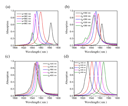
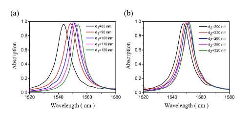
Fig.4d shows that the almost perfect absorption of monolayer graphene and the absorption wavelengths are linearly tuned by the thickness of PMMA (). The spectra lines are red-shifted from nm to nm as increases from nm to nm. The spectral selectivity of the structure is improved by adjusting the thickness of PMMA (), and the feasibility of the experiment is also provided for the designed in the paper[25]. In addition, the influence of the thickness of Si () and SiO2 () layers in the Bragg mirror are also investigated, as shown in Fig.5a and b, respectively. The peaks of the absorption spectra of monolayer graphene are linearly red-shifted with the increase of the thickness of Si and SiO2 due to the change of the gap position, in which the effect of Si are relatively obvious[26], as can be seen in Fig.5a. Theoretically, the peaks wavelength of the absorption spectra of graphene can be approximately calculated by the equation , where and are the effective refractive index of Si and SiO2 in the Bragg mirror, respectively. From the formula above, we can see that the thickness of Si has a greater influence on the peaks wavelength () than the SiO2 layers thickness. But they have minimal effect on the peaks magnitude of the absorption spectra of graphene.
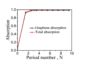
As depicted in Fig.6, we simulate the absorption of monolyer-graphene (black line) and the whole structure (red line) with increasing the period number () of the Bragg mirror. It can be found that when the number of period , the perfect absorption of the graphene layer can achieve, and then the system almost tends to be stable with the increases continuously.
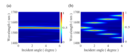
Until now, we investigate the various properties of the designed structure at normal incidence. Subsequently, in Fig.7 we show the absorption of the graphene layer as functions of the incident angle and wavelength for TM polarization and TE polarization. As shown in Fig.7a, the wavelengths of the major absorption peaks are almost unchanged with the increase of the incident angle continuously for TM-polarized, mainly due to the insensitivity of the guided mode resonance to the incident angle, it can be valuable in applications on integrated optoelectronic devices. In contrast, as for the TE-polarized, when the incident light is tilted at a certain angle, another resonant mode is stimulated by the incident light, resulting in an additional graphene absorption peak appearing on the absorption spectrum in Fig.7b. Meanwhile, the wavelengths of two graphene absorption peaks are also changing with increasing the tilt angle of incident light. Therefore, we have proved that the designed structure can simultaneously achieve the critical coupling of multiple resonances, which is a major technical index of multispectral optical detection. And these angular characteristics of the structure have potential applications in the field of space optical measurement[27].
4 Conclusions
In summary, we investigate a monolayer graphene-based perfect absorption structure with a cross-shaped groove air resonator, in which the absorption of graphene can achieve total absorption (about of the incident light at normal incidence) at telecommunication wavelengths through the mechanism of critical coupling with guided resonance. The modeling work implies that the absorption wavelength of monolayer graphene can be tuned by adjusting the parameters of structure. In other words, the perfect absorption efficiency and spectral selectivity are obtained with attaining critical coupling condition. The results of research work also show that the different polarization modes (TM or TE) have different sensitivity to the incident angle, which lead to their different incident angular tolerance. In addition, the proposed graphene-based perfect absorption structure with a dielectric Bragg mirror together with its design principle can be extended to enhance the absorption of other two-dimensional materials.
5 Acknowledgements
The author Xiaoyun Jiang (XYJIANG) expresses her deepest gratitude to her Ph.D. advisor Tao Wang for providing guidance during this project. This work is supported by the National Natural Science Foundation of China (Grant No. 61376055, 61006045 and 61775064), and the Fundamental Research Funds for the Central Universities (HUST: 2016YXMS024).