Dry-transferred CVD graphene for inverted spin valve devices
Abstract
Integrating high-mobility graphene grown by chemical vapor deposition (CVD) into spin transport devices is one of the key tasks in graphene spintronics. We use a van der Waals pickup technique to transfer CVD graphene by hexagonal boron nitride (hBN) from the copper growth substrate onto predefined Co/MgO electrodes to build inverted spin valve devices. Two approaches are presented: (i) a process where the CVD-graphene/hBN stack is first patterned into a bar and then transferred by a second larger hBN crystal onto spin valve electrodes and (ii) a direct transfer of a CVD-graphene/hBN stack. We report record high spin lifetimes in CVD graphene of up to at room temperature. Overall, the performances of our devices are comparable to devices fabricated from exfoliated graphene also revealing nanosecond spin lifetimes. We expect that our dry transfer methods pave the way towards more advanced device geometries not only for spintronic applications but also for CVD-graphene-based nanoelectronic devices in general where patterning of the CVD graphene is required prior to the assembly of final van der Waals heterostructures.
pacs:
73.40.-c, 75.70.Cn, 75.76.+j, 81.05.ue, 81.15.GhDry transfer techniques have become a key technology for building high-quality van der Waals heterostructures from 2D materials.Wang et al. (2013); Butler et al. (2013); Kretinin et al. (2014); Geim and Grigorieva (2013); Castellanos-Gomez et al. (2014); Zomer et al. (2011) For example, this technique allows to fully encapsulate graphene between two insulating hexagonal boron nitride (hBN) crystals serving as excellent substrates for graphene.Dean et al. (2010) Additionally, the graphene gets fully protected against air contaminations and is not exposed to wet chemistry which allows to unveil unique electronic properties with charge carrier mobilities exceeding at cryogenic temperatures.Wang et al. (2013) This technique has also been adopted for single and bilayer graphene grown by chemical vapor deposition (CVD)Banszerus et al. (2015); Schmitz et al. (2017) and it was demonstrated that the CVD graphene transport properties are equivalent to devices based on high-mobility exfoliated graphene.Banszerus et al. (2015, 2016); Schmitz et al. (2017)
In graphene spintronics,Han et al. (2014); Roche et al. (2015) there has also been a tremendous improvement in spin and charge transport properties when using the van der Waals pick-up approach to protect graphene by hBN.Drögeler et al. (2014, 2016); Ingla-Aynés, Meijerink, and Wees (2016); Avsar et al. (2016); Guimarães et al. (2014); Zomer et al. (2012); Gurram et al. (2016) The best device performance so far has been achieved for exfoliated graphene which gets picked up by a large hBN crystal and is subsequently transferred on prepatterned Co/MgO electrodes yielding spin lifetimes of , spin diffusion lengths of combined with charge carrier mobilities of more than at room temperature.Drögeler et al. (2016)
In contrast, state-of-the-art CVD graphene-based spin valve devices exhibit minor charge and spin transport properties with spin lifetimes typically below and carrier mobilities up to .Avsar et al. (2011); Kamalakar et al. (2015); Stecklein et al. (2016) This is mainly caused by the wet transfer process which is used to delaminate CVD graphene from the growth substrate (Cu foil). Longer spin lifetimes () could only be measured in devices with long spin transport channel lengths () where the influence of contact-induced spin scattering Maassen et al. (2012); Volmer et al. (2015); Amamou et al. (2016); Stecklein et al. (2016) gets diminished.
In this Letter we show inverted spin valve devices based on dry-transferred CVD graphene. First (i) we utilize a two-step fabrication process providing bar-shaped CVD graphene: Therefore we use a first hBN crystal to delaminate CVD graphene (Gr) from the Cu foil (Fig. 1a). As the CVD graphene gets ripped along the outer edges of the hBN crystal, this CVD-graphene/hBN stack is transferred onto a Si/SiO2 substrate where we etch a well-defined bar (Fig. 1b) through the whole heterostructure by reactive ion etching (RIE). In a next step we pick up the CVD-graphene/hBN bar with a second hBN crystal (Fig. 1c) and place the whole stack onto prepatterned Co/MgO electrodes (see Figs. 1d,1f). Throughout the whole process the CVD graphene is protected by the hBN against solvents, polymers and the metal hard mask which is used for etching. We also use a second approach (ii) where the picked-up CVD-graphene/hBN stack is directly transferred onto the spin valve electrodes (see Fig. 1g). All devices show comparable spin transport properties as devices based on exfoliated graphene.
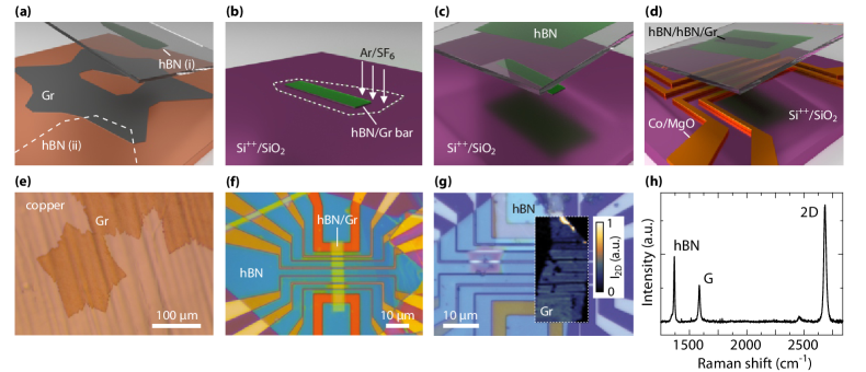
We fabricate CVD-graphene-based inverted spin valves by first defining magnetic electrodes on a Si++/SiO2 () substrate (see Fig. 1d) using standard electron beam lithography (EBL), molecular beam epitaxy (MBE) and a lift-off process. They consist of Co followed by of MgO. The latter is used as a spin injection and detection barrier. Graphene is grown by low pressure chemical vapor deposition on the inside of copper enclosures which typically results in large graphene flakes of up to a few hundred micrometers (see Fig. 1e). Process details are given in Ref. [8]. The flakes are stored under ambient conditions for some days to allow for oxidation along the copper-to-graphene interface. This oxidation weakens the graphene-to-copper adhesion which allows subsequent pick-up of the CVD graphene by hBN. Banszerus et al. (2015) We first focus on the process to fabricate bar-shape CVD-graphene/hBN structures. For this, we pick-up the CVD graphene from the copper foil (Fig. 1a) by using hBN which was exfoliated onto a stack of polydimethylsiloxane (PDMS), polyvinylalcohol (PVA) and polymethylmethacrylate (PMMA). Thereafter, we place the graphene/hBN stack on a clean Si/SiO2 chip and dissolve the polymer stack in deionized (DI) water, acetone and isopropanol. The desired shape of the graphene/hBN stack is defined by an aluminum hardmask made by EBL and a lift-off process and subsequently etched by RIE in an Ar/SF6 plasma (Fig. 1b). After the etching, the aluminum is removed using tetramethylammonium hydroxide (TMAH) and thereafter washed with DI water. During the whole process of patterning the graphene is protected by the overlying hBN crystal. For the final transfer we exfoliate an additional hBN flake on a PMMA membrane which we use to pick up the graphene/hBN bar (Fig. 1c). In a last step the graphene/hBN/hBN stack is deposited onto the Co/MgO electrodes (Fig. 1d) and the polymer membrane is dissolved in acetone and isopropanol. An optical image of a finished device is shown in Fig. 1f. The yellow stripe in the center of the electrode structure represents the patterned graphene/hBN bar which was transferred by a larger hBN crystal which shows up as the blue large flake.
We note that the pick-up of the etched graphene/hBN stack is not as simple as for unpatterned graphene/hBN, which likely may be caused by residues stemming either from the hard mask or from organic solvents which are present on top of the hBN. Apparently, this leads to an overall weaker adhesion to the hBN which is used for the pick-up. Another observation is that the supporting PMMA membrane starts to corrugate when it gets retracted from the substrate during the pick-up of the graphene/hBN stack (Fig. 1c). We suspect that the membrane has a strong adhesion to the substrate due the etching of its surface by the RIE process (Fig. 1b) which results in irreversible stretching when retracting the membrane. The corrugations in the membrane may prevent that the hBN/hBN/graphene smoothly adapt to the electrode structure of the spin valve devices (Fig. 1d). Hence, the hBN/hBN/graphene stacks may float away or get partially lifted when the membrane is dissolved. During this procedure residues from the fabrication process of the electrodes may bond to graphene and reduce its electronic quality.To allow for a better adhesion of the supporting hBN crystal to both the electrodes and the substrates we heat the whole sample beyond the glass temperature of the PMMA () prior to the dissolving of the membrane.
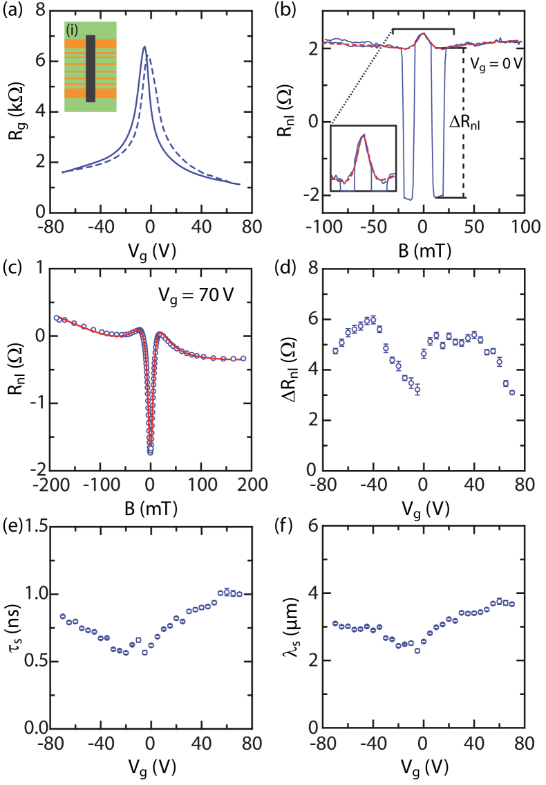
We next focus of typical charge and spin transport properties obtained from such devices. All measurements were carried out under vacuum conditions at room temperature using standard low frequency lock-in techniques.Volmer et al. (2013) The measured gate dependent graphene resistance is shown in Fig. 2a. From this curve we extract a charge carrier mobility of . In contrast, devices where we did not need to apply the additional heating procedure exhibit mobilities of . However, the latter set of devices suffer from an improper mechanical contact of the hBN/hBN/graphene stack to the substrate which results in maximum spin lifetimes of only several hundred picoseconds most likely due to the ingress of solvents during the final fabrication step. This general trend was also observed in devices with exfoliated graphene. Drögeler et al. (2016)
Fig. 2b shows spin valve measurements recorded on a spin transport region with . The data were taken in non-local geometry with an in-plane magnetic field applied along the electrode direction. The spin amplitude , which is given by the non-local resistance between parallel and anti-parallel alignments of the magnetization direction of the spin injection and detection electrodes, typically is on the order of several Ohms. Next to the switching there is a small peak around zero magnetic field which is symmetric in magnetic field. We attribute this to Hanle spin precession caused by an electrode magnetization direction which is not collinear with the electrode direction. The red curve in Fig. 2b is a fit by the standard Hanle model Drögeler et al. (2016); Johnson and Silsbee (1988); Fabian et al. (2007) and describes the data quite well even towards larger fields. It is now interesting to compare the extracted spin lifetime of and the spin diffusion length of with values obtained from standard Hanle spin precession measurements, where the magnetic field is applied perpendicular to the graphene sheet. Fig. 2c shows a typical Hanle curve for anti-parallel alignment of the magnetization directions. Gate dependent spin amplitude , spin lifetime and spin diffusion length are depicted in Figs. 2d-f. The spin amplitude first increases away from the CNP and decreases again for high values of the gate voltage . As for most of the exfoliated samples both and increase for larger gate voltages,Drögeler et al. (2016); Guimarães et al. (2014); Volmer et al. (2013); Han and Kawakami (2011); Han et al. (2012); Yang et al. (2011) i.e. larger carrier densities with the former reaching a maximum value of . We note that the respective spin transport parameters for match quite well to the above values which confirms our notion that the peak in the spin valve measurement indeed can be interpreted as a Hanle curve caused by perpendicularly oriented magnetic domains. They may have been formed when the sample was heated during the deposition of the hBN/hBN/graphene stack. The magnetization configuration is rather stable and cannot be changed even in large magnetic fields of up to . This important finding indicates that the in-plane and out-of-plane spin lifetimes are equal and excludes significant influences of Rashba spin orbit coupling (SOC) in this device. A similar conclusion was obtained from spin transport studies on exfoliated graphene flakes where the spin lifetime anisotropy was determined by spin precession in a tilted magnetic field.Raes et al. (2016) Our results demonstrate that the transfer and etching technique allows to achieve nanosecond spin lifetimes even for CVD graphene devices with short spin transport lengths.
We also investigated a second (ii) fabrication method which we call the stamping technique. Here, we mechanically stamp-out a CVD graphene stripe from the edge of the flake. Again, we first exfoliate hBN on a stack of PMMA/PVA/PDMS. For the stamping the respective edges of the CVD and the hBN crystal are aligned in such a way that the overlap region of both flakes defines a stripe in the CVD graphene (see dashed line in Fig. 1a and label "hBN (ii)"). The pick-up of the stripe is feasible since there is only a strong adhesion between graphene and hBN but not between PMMA and graphene. Thereafter, the stack of PDMS/PVA/PMMA/hBN/graphene is aligned and transferred to a predefined Co/MgO electrode structure. In a last step the whole stack is put in acetone and isopropanol to remove the polymer.
An optical image of the final device is shown in Fig. 1g. Additionally, we include an intensity map of the Raman 2D-peak of the CVD graphene to identify both the position and the shape of the graphene. The averaged spectrum of the Raman map is depicted in Fig. 1h exhibiting a 2D line width of demonstrating the high electronic quality of the transferred CVD graphene.Banszerus et al. (2017)
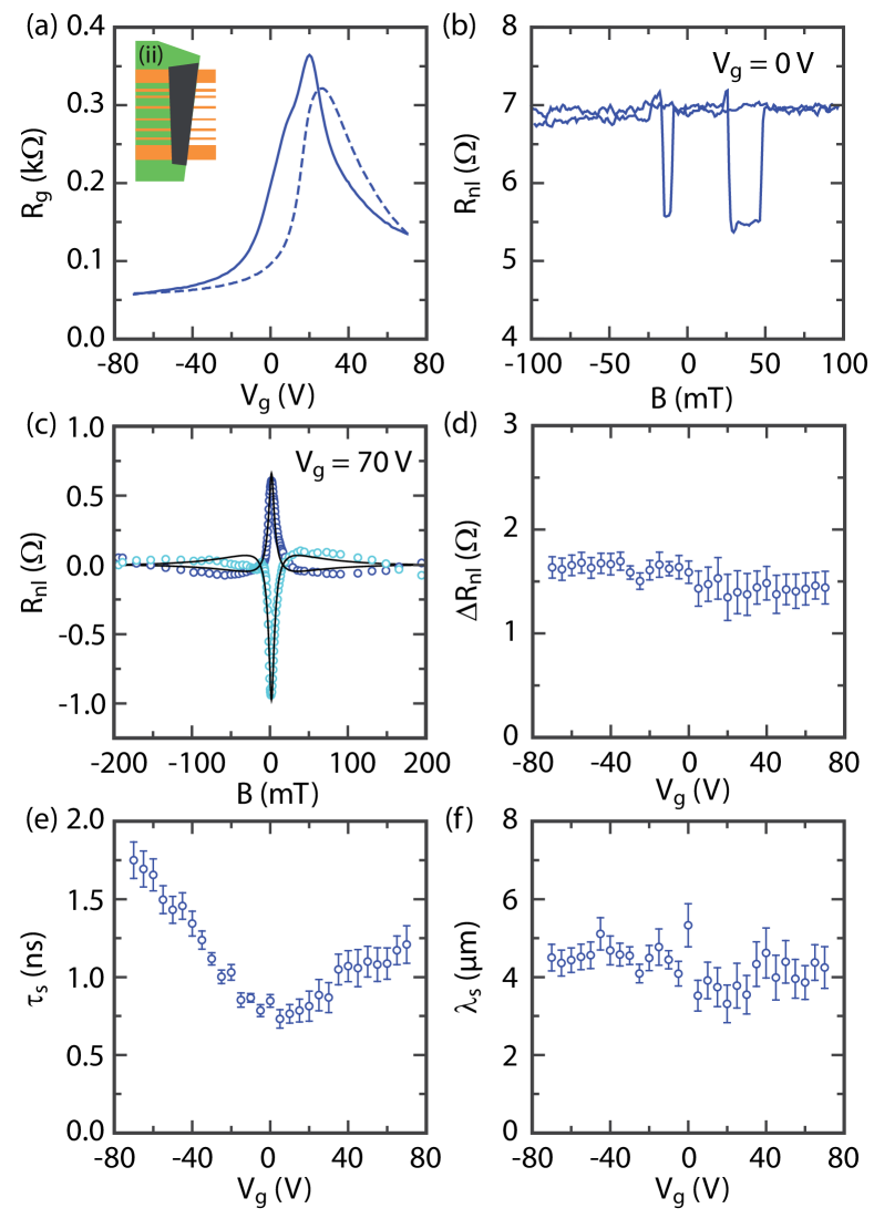
In Fig. 3a we plot the graphene resistance as a function of back gate voltage for the device shown in Fig. 1g. The room temperature electron mobility is larger than for the device in Fig. 2 and is in the same order as for inverted spin valve devices with exfoliated graphene. The spin valve curve and typical Hanle spin precession curves for both parallel and antiparallel alignments are shown in Fig. 3b and Fig. 3c, respectively. We note that there is a small contribution from an antisymmetric Hanle curve which is expected if the magnetization directions of both spin injection and detection electrodes are not perfectly colinear. We consider this contribution when fitting the curves by the standard Hanle model.Drögeler et al. (2016) The gate dependence of the extracted , and values are shown in Figs. 3d-f. Both the spin amplitude and the spin diffusion length are almost independent of the gate voltage while the spin lifetime again shows the well-know V-shape dependence with spin lifetimes reaching . This value is the longest spin lifetime measured for CVD graphene by now and compares well to the average values obtained for inverted spin valve devices where we used exfoliated flakes.Drögeler et al. (2016)
In summary, we have demonstrated two dry transfer methods for integrating CVD graphene in inverted spin valve devices. Both allow for spin lifetimes in the nanosecond regime at room temperature and high charge carrier mobilities. Although both methods still have room for improvements our findings show that the device performance of CVD-graphene-based spin transport devices is well comparable with that of state-of-the-art exfoliated graphene-based devices. Most importantly, the nanosecond spin lifetimes indicate that there is no significant spin scattering at, for examples, copper residues on the surface of the transferred CVD graphene which might be expected to result from CVD growth in the copper enclosures.Balakrishnan et al. (2014); Frank et al. (2017) We expect that the presented fabrication methods pave the way towards more advanced device geometries not only for spintronic applications but also for CVD-graphene-based nanoelectronic devices in general.
Acknowledgements.
We acknowledge funding from the European Union Seventh Framework Programme under Grant Agreement No. 604391 Graphene Flagship and the Deutsche Forschungsgemeinschaft (BE 2441/9-1) and support by the Helmholtz Nano Facility (HNF)HNF at the Forschungszentrum Jülich. Growth of hexagonal boron nitride crystals was supported by the Elemental Strategy Initiative conducted by the MEXT, Japan and JSPS KAKENHI Grant Numbers JP26248061, JP15K21722 and JP25106006.References
- Wang et al. (2013) L. Wang, I. Meric, P. Y. Huang, Q. Gao, Y. Gao, H. Tran, T. Taniguchi, K. Watanabe, L. M. Campos, D. A. Muller, J. Guo, P. Kim, J. Hone, K. L. Shepard, and C. R. Dean, Science 342, 614 (2013), http://www.sciencemag.org/content/342/6158/614.full.pdf .
- Butler et al. (2013) S. Z. Butler, S. M. Hollen, L. Cao, Y. Cui, J. A. Gupta, H. R. Gutiérrez, T. F. Heinz, S. S. Hong, J. Huang, A. F. Ismach, E. Johnston-Halperin, M. Kuno, V. V. Plashnitsa, R. D. Robinson, R. S. Ruoff, S. Salahuddin, J. Shan, L. Shi, M. G. Spencer, M. Terrones, W. Windl, and J. E. Goldberger, ACS Nano 7, 2898 (2013), http://dx.doi.org/10.1021/nn400280c .
- Kretinin et al. (2014) A. V. Kretinin, Y. Cao, J. S. Tu, G. L. Yu, R. Jalil, K. S. Novoselov, S. J. Haigh, A. Gholinia, A. Mishchenko, M. Lozada, T. Georgiou, C. R. Woods, F. Withers, P. Blake, G. Eda, A. Wirsig, C. Hucho, K. Watanabe, T. Taniguchi, A. K. Geim, and R. V. Gorbachev, Nano Lett. 14, 3270 (2014), http://dx.doi.org/10.1021/nl5006542 .
- Geim and Grigorieva (2013) A. K. Geim and I. V. Grigorieva, Nature 499, 419 (2013).
- Castellanos-Gomez et al. (2014) A. Castellanos-Gomez, M. Buscema, R. Molenaar, V. Singh, L. Janssen, H. S. J. van der Zant, and G. A. Steele, 2D Mater. 1, 011002 (2014).
- Zomer et al. (2011) P. J. Zomer, S. P. Dash, N. Tombros, and B. J. van Wees, Phys. Rev. Lett. 99, 232104 (2011).
- Dean et al. (2010) C. Dean, A. Young, I. Meric, C. Lee, L. Wang, S. Sorgenfrei, K. Watanabe, T. Taniguchi, P. Kim, K. L. Shepard, and J. Hone, Nat. Nanotech. 5, 722 (2010).
- Banszerus et al. (2015) L. Banszerus, M. Schmitz, S. Engels, J. Dauber, M. Oellers, F. Haupt, K. Watanabe, T. Taniguchi, B. Beschoten, and C. Stampfer, Sci. Adv. 1, e1500222 (2015), http://advances.sciencemag.org/content/1/6/e1500222.full.pdf .
- Schmitz et al. (2017) M. Schmitz, S. Engels, L. Banszerus, K. Watanabe, T. Taniguchi, C. Stampfer, and B. Beschoten, Appl. Phys. Lett. 110, 263110 (2017).
- Banszerus et al. (2016) L. Banszerus, M. Schmitz, S. Engels, M. Goldsche, K. Watanabe, T. Taniguchi, B. Beschoten, and C. Stampfer, Nano Lett. 16, 1387 (2016), http://dx.doi.org/10.1021/acs.nanolett.5b04840 .
- Han et al. (2014) W. Han, R. K. Kawakami, M. Gmitra, and J. Fabian, Nat. Nanotechnol. 9, 794 (2014).
- Roche et al. (2015) S. Roche, J. Åkerman, B. Beschoten, J.-C. Charlier, M. Chshiev, S. P. Dash, B. Dlubak, J. Fabian, A. Fert, M. Guimaraes, F. Guinea, I. Grigorieva, C. Schönenberger, P. Seneor, C. Stampfer, S. O. Valenzuela, X. Waintal, and B. van Wees, 2D Mater. 2, 030202 (2015).
- Drögeler et al. (2014) M. Drögeler, F. Volmer, M. Wolter, B. Terres, K. Watanabe, T. Taniguchi, G. Güntherodt, C. Stampfer, and B. Beschoten, Nano Lett. 14, 6050 (2014).
- Drögeler et al. (2016) M. Drögeler, C. Franzen, F. Volmer, T. Pohlmann, L. Banszerus, M. Wolter, K. Watanabe, T. Taniguchi, C. Stampfer, and B. Beschoten, Nano Lett. 16, 3533 (2016), http://dx.doi.org/10.1021/acs.nanolett.6b00497 .
- Ingla-Aynés, Meijerink, and Wees (2016) J. Ingla-Aynés, R. J. Meijerink, and B. J. v. Wees, Nano Lett. 16, 4825 (2016).
- Avsar et al. (2016) A. Avsar, I. J. Vera-Marun, J. Y. Tan, G. K. W. Koon, K. Watanabe, T. Taniguchi, S. Adam, and B. Özyilmaz, NPG Asia Mater. 8, e274 (2016).
- Guimarães et al. (2014) M. H. D. Guimarães, P. J. Zomer, J. Ingla-Aynés, J. C. Brant, N. Tombros, and B. J. van Wees, Phys. Rev. Lett. 113, 086602 (2014).
- Zomer et al. (2012) P. J. Zomer, M. H. D. Guimarães, N. Tombros, and B. J. van Wees, Phys. Rev. B 86, 161416 (2012).
- Gurram et al. (2016) M. Gurram, S. Omar, S. Zihlmann, P. Makk, C. Schönenberger, and B. J. van Wees, Phys. Rev. B 93, 115441 (2016).
- Avsar et al. (2011) A. Avsar, T.-Y. Yang, S. Bae, J. Balakrishnan, F. Volmer, M. Jaiswal, Z. Yi, S. R. Ali, G. Güntherodt, B. H. Hong, B. Beschoten, and B. Özyilmaz, Nano Lett. 11, 2363 (2011).
- Kamalakar et al. (2015) M. V. Kamalakar, C. Groenveld, A. Dankert, and S. P. Dash, Nat. Commun. 6, 6766 (2015).
- Stecklein et al. (2016) G. Stecklein, P. A. Crowell, J. Li, Y. Anugrah, Q. Su, and S. J. Koester, Phys. Rev. Appl. 6, 054015 (2016).
- Maassen et al. (2012) T. Maassen, I. J. Vera-Marun, M. H. D. Guimarães, and B. J. van Wees, Phys. Rev. B 86, 235408 (2012).
- Volmer et al. (2015) F. Volmer, M. Drögeler, T. Pohlmann, G. Güntherodt, C. Stampfer, and B. Beschoten, 2D Mater. 2, 024001 (2015).
- Amamou et al. (2016) W. Amamou, Z. Lin, J. van Baren, S. Turkyilmaz, J. Shi, and R. K. Kawakami, APL Mater. 4, 032503 (2016).
- Volmer et al. (2013) F. Volmer, M. Drögeler, E. Maynicke, N. von den Driesch, M. L. Boschen, G. Güntherodt, and B. Beschoten, Phys. Rev. B 88, 161405 (2013).
- Johnson and Silsbee (1988) M. Johnson and R. H. Silsbee, Phys. Rev. B 37, 5312 (1988).
- Fabian et al. (2007) J. Fabian, A. Matos-Abiague, C. Ertler, P. Stano, and I. Žutić, Acta Phys. Slovaca 57, 565 (2007).
- Han and Kawakami (2011) W. Han and R. K. Kawakami, Phys. Rev. Lett. 107, 047207 (2011).
- Han et al. (2012) W. Han, J.-R. Chen, D. Wang, K. M. McCreary, H. Wen, A. G. Swartz, J. Shi, and R. K. Kawakami, Nano Lett. 12, 3443 (2012).
- Yang et al. (2011) T.-Y. Yang, J. Balakrishnan, F. Volmer, A. Avsar, M. Jaiswal, J. Samm, S. R. Ali, A. Pachoud, M. Zeng, M. Popinciuc, G. Güntherodt, B. Beschoten, and B. Özyilmaz, Phys. Rev. Lett. 107, 047206 (2011).
- Raes et al. (2016) B. Raes, J. E. Scheerder, M. V. Costache, F. Bonell, J. F. Sierra, J. Cuppens, J. Van de Vondel, and S. O. Valenzuela, Nat. Commun. 7, 11444 (2016).
- Banszerus et al. (2017) L. Banszerus, H. Janssen, M. Otto, A. Epping, T. Taniguchi, K. Watanabe, B. Beschoten, D. Neumaier, and C. Stampfer, 2D Mater. 4, 025030 (2017).
- Balakrishnan et al. (2014) J. Balakrishnan, G. K. W. Koon, A. Avsar, Y. Ho, J. H. Lee, M. Jaiswal, S.-J. Baek, J.-H. Ahn, A. Ferreira, M. A. Cazalilla, A. H. Castro Neto, and B. Özyilmaz, Nat. Commun. 5, 4748 (2014).
- Frank et al. (2017) T. Frank, S. Irmer, M. Gmitra, D. Kochan, and J. Fabian, Phys. Rev. B 95, 035402 (2017).
- (36) Forschungszentrum Jülich GmbH. HNF - Helmholtz Nano Facility. Journal of large-scale research facilities, 3, A112 (2017).