C4N3H monolayer: A novel two-dimensional organic Dirac material with high Fermi velocity
Abstract
Searching for two-dimensional (2D) organic Dirac materials, which have more adaptable practical applications in comparing with inorganic ones, is of great significance and has been ongoing. However, only two kinds of these materials with low Fermi velocity have been discovered so far. Herein, we report the design of an organic monolayer with C4N3H stoichiometry which possesses fascinating structure and good stability in its free-standing state. More importantly, we demonstrate that this monolayer is a semimetal with anisotropic Dirac cones and very high Fermi velocity. This Fermi velocity is roughly one order of magnitude larger than that in 2D organic Dirac materials ever reported, and is comparable to that in graphene. The Dirac states in this monolayer arise from the extended -electron conjugation system formed by the overlapping 2pz orbitals of carbon and nitrogen atoms. Our finding opens a door for searching more 2D organic Dirac materials with high Fermi velocity.
pacs:
I introduction
Following with the great development of graphene 1 and topological insulators 2 , an emerging field of Dirac physics is being established for investigating the quantum relativistic properties of a class of special materials with Dirac cones, namely Dirac materials 3 . Such materials exhibit linear electronic band dispersion at the Fermi level, that is Dirac band, and thus have charge carriers behaved like massless Dirac fermions. The unique Dirac bands endow these materials with many novel phenomena in electronic transport, such as ballistic charge transport and high carrier mobility 4 , Klein tunneling 5 , various quantum Hall effects 1 ; 6 ; 7 , etc. These specific transport properties offer Dirac materials a wide range of promising applications in high-speed low-dissipation devices. In addition, the continuous reduction in the size of devices highly needs to develop low-dimensional materials. Thus, two-dimensional (2D) Dirac materials are much more desirable for the applications in nanoscale integrated circuits.
Theoretically, based on the generalized von Neumann-Wigner theorem 8 , at least three conditions are required to achieve Dirac bands in 2D materials: (i) specific symmetries, (ii) proper parameters and (iii) appropriate Fermi level and band overlap 9 . The hexagonal symmetry was widely believed to the most favorable for the existence of Dirac bands due to the fact that many 2D Dirac materials are observed in hexagonal lattice. However, it is not a necessary precondition for the presence of 2D Dirac materials. For example, 6,6,12-graphyne 10 , square-MoS2 11 and Pmmn-boron 12 have rectangular lattices while also possess Dirac cones. Besides symmetries, proper structure parameters such as bond lengths and angles, which are related to the crystal lattice, are also required. Furthermore, the Fermi level should precisely lie at the Dirac points, while there should be not any other bands overlap at the Fermi level. This condition is required to ensure the experimental observation and practical applications of the novel properties particular to the Dirac cones. Unfortunately, 2D Dirac materials are found to be very rare due to these rigorous conditions 9 . For instance, among hundreds of 2D materials, only graphene 1 ; 4 , phagraphene 13 , graphynes 10 , silicene and germanen 14 , borophenes 12 , FeB2 monolaye 15 , etc., have been confirmed to be 2D Dirac materials. Moreover, most of the existing 2D Dirac materials are inorganic compounds. In general, organic materials have the additional advantages of mechanical flexibility and tunable properties in comparison with inorganic ones. Therefore, it is of great practical significance to search for more 2D organic Dirac materials with the development of Dirac physics .
Actually, an extensive search for 2D organic Dirac materials has been ongoing. However, to the best of our knowledge, only two kinds of 2D organic systems have been discovered to be Dirac materials so far. The first successfully realized example is the 2D layered organic conductor -(BEDT-TTF)2I3 (BEDT-TTF = bis(ethylenedithio)-tetrathiafulvalene) which turns into a Dirac material with a pair of titled Dirac cones when applying a high hydrostatic pressure above 1.2 GPa 16 ; 17 . The other one is a theoretical design about some 2D conjugated polymers. These polymers can be theoretically constructed by replacing the insulating connectors (1,3,5-triazine, etc.) of conventional semiconducting 2D covalent organic frameworks (COFs) with the conductive ones (trivalent carbon atoms, etc.) 18 . Unfortunately, both of the two kinds of 2D organic materials have very low Fermi velocities, which are roughly one order of magnitude lower than that in 2D inorganic Dirac materials 4 ; 10 ; 12 ; 13 ; 14 ; 15 . It is known that a high Fermi velocity is favorable to the transport property of a Dirac material 19 . Thus, designing stable 2D organic Dirac materials with high Fermi velocities is urgent and of great practical significance.
Inspired by the experimental synthesis of several 2D carbon nitride sheets, such as graphitic carbon nitride (g-C3N4) 20 ; 21 , C2N holey 2D crystal (C2N-h2D) 22 and C3N sheets 23 based on condensation reactions, we design a novel 2D organic material named as C4N3H monolayer by its stoichiometry. This organic monolayer has a intriguing structure with evenly distributed heart-shaped angstrom-scale pores and rather good dynamic, thermal and mechanical stabilities in its freestanding state. More interestingly, we demonstrate that this organic monolayer is a 2D Dirac material with anisotropic Dirac cones and a very high Fermi velocity of m s-1. Remarkably, this Fermi velocity is roughly one order of magnitude larger than that in 2D organic Dirac materials ever reported 17 ; 18 , and is even comparable to that in 2D inorganic Dirac materials 4 ; 10 ; 12 ; 13 ; 14 ; 15 . The Dirac points in this monolayer locate at off-symmetry points between the and K points, and arise predominantly from the overlapping 2pz orbitals of carbon (C) and nitrogen (N) atoms. In addition, we also comment on the experimental feasibility of producing the predicted C4N3H monolayer and propose two hypothetical synthesis routes.
II Computational Details
Structural optimization, energy, density of states (DOS), band structure, electron localization function (ELF) 24 and deformation charge density calculations based on density functional theory were performed in the framework of the generalized gradient approximation with the PBE functional 25 using Vienna ab initio simulation package (VASP) 26 ; 27 . Projector-augmented plane wave approach 28 was used to represent the electron interaction. A 500 eV energy cutoff of the plane-wave basis sets and the first Brillouin zone sampled with a Monkhorst-Pack k-points grid were adopted in the structural relaxations and self-consistent calculations. In all the calculations, a vacuum distance of 15 Å was applied along the perpendicular direction to ensure negligible interaction between adjacent layers. All atoms were allowed to relax without any constraint in the geometric optimizations until the total energy change was less than eV and the force on each atom was smaller than 0.001 eV Å-1. According to the crystal symmetry, the band structure of the C4N3H monolayer was calculated along the special lines connecting the following high-symmetry points: (0, 0, 0), K (0.4, 0.4, 0), M (0.5, 0, 0), R (0.6, -0.4, 0), S (0.5, -0.5, 0), (0, 0, 0), and M (0.5, 0, 0) in the k-space. Moreover, to confirm the existence of Dirac states, the band structure of the C4N3H monolayer was also recomputed respectively by the more accurate Heyd-Scuseria-Ernzerhof (HSE06) functional 29 and the spin-orbit coupling (SOC) effect.
The finite displacement method, as implemented in the phonopy code 30 , was employed to calculate the phonon dispersion curves of the C4N3H monolayer. During the phonon spectrum calculation, a supercell was employed and the force constant matrix was determined by the VASP. First-principles molecular dynamics (FPMD) simulations, as also performed in the VASP, were employed to evaluate the thermal stability of this monolayer. The initial configuration with a supercell was annealed at different temperatures of 300, 500 and 1000 K, respectively. The temperature was controlled by the Nosé-Hoover thermostat 31 . At each temperature, FPMD simulations in NVT ensemble lasted for 30 ps with a time step of 2.0 fs. A kinetic energy cutoff of 450 eV and the PBE functional were employed in all FPMD simulations.
III Results and Discussion
III.1 Geometric structure of the C4N3H monolayer
Figures 1(a) and 1(b) respectively present the top and side views of the geometric structure for the optimized C4N3H monolayer. As shown in Fig. 1(a), this monolayer has a rhombic primitive cell (represented by the green dash lines) with the fully relaxed lattice constants a1 = a2 = 4.77 Å, (angle between the a1 and a2 lattice vectors). Obviously, its primitive cell consists of four C atoms, three N atoms and one H atom. The correspondingly optimized lattice constants of the transformed rectangular conventional cell [denoted by the blue dash lines in Fig. 1(a)] with the same symmetry are a = 7.54 Å and b = 5.84 Å, respectively. This structure has the symmetry of and belongs to the space group of Amm2. It is obvious that angstrom-scale pores evenly distribute in the structure of the C4N3H monolayer. Intriguingly, if we link the atoms around the angstrom-scale pore in its conventional cell one by one, the connecting line shows a perfect heart-shape [denoted by the red solid line in Fig. 1(a)]. By anatomizing this intriguing structure, one can find that this monolayer is actually constructed by using N atoms to link the framework of pyrrole molecules [represented by the pink dash lines in Fig. 1(a)]. As shown in Fig. 1(a), we label the N atoms in the framework of pyrrole molecules as N1, and the ones sited at the linking positions as N2. There are also two kinds of C atoms, i) the C atoms with the nearest neighbors of two C atoms and one N atom (labeled as C1), and ii) the rest of C atoms which has one C atom and two N atoms as the nearest neighbors (labeled as C2). The C1–C1 and C1–C2 bond lengths (1.43 and 1.46 Å, respectively) are only slightly larger than that in graphene (1.42 Å, a typical bond length for sp2 C–C bonds), and are noticeably smaller than 1.54 Å (the standard value of C–C bond length for sp3 hybridization) 32 . The lengths of C1–N2, C2–N1, and C2–N2 bonds in this monolayer are respectively about 1.33, 1.38 and 1.31 Å, very similar to that in the already-synthesized g-C3N4 (ca. 1.33 and 1.41 Å) 21 and C2N-h2D (1.33 Å) 22 which have stable structures with sp2 hybridization bonds. More detailed information about the structural properties is summarized in Fig. 1 of the Supplemental Material 33 . In addition, it is noteworthy that the C4N3H monolayer has an exactly planar structure, as shown in Fig. 1(b). This exactly planar structure and the features of bond lengths and bond angles imply that the chemical bonds in this monolayer ought to be covalent bonds with sp2 hybridization.
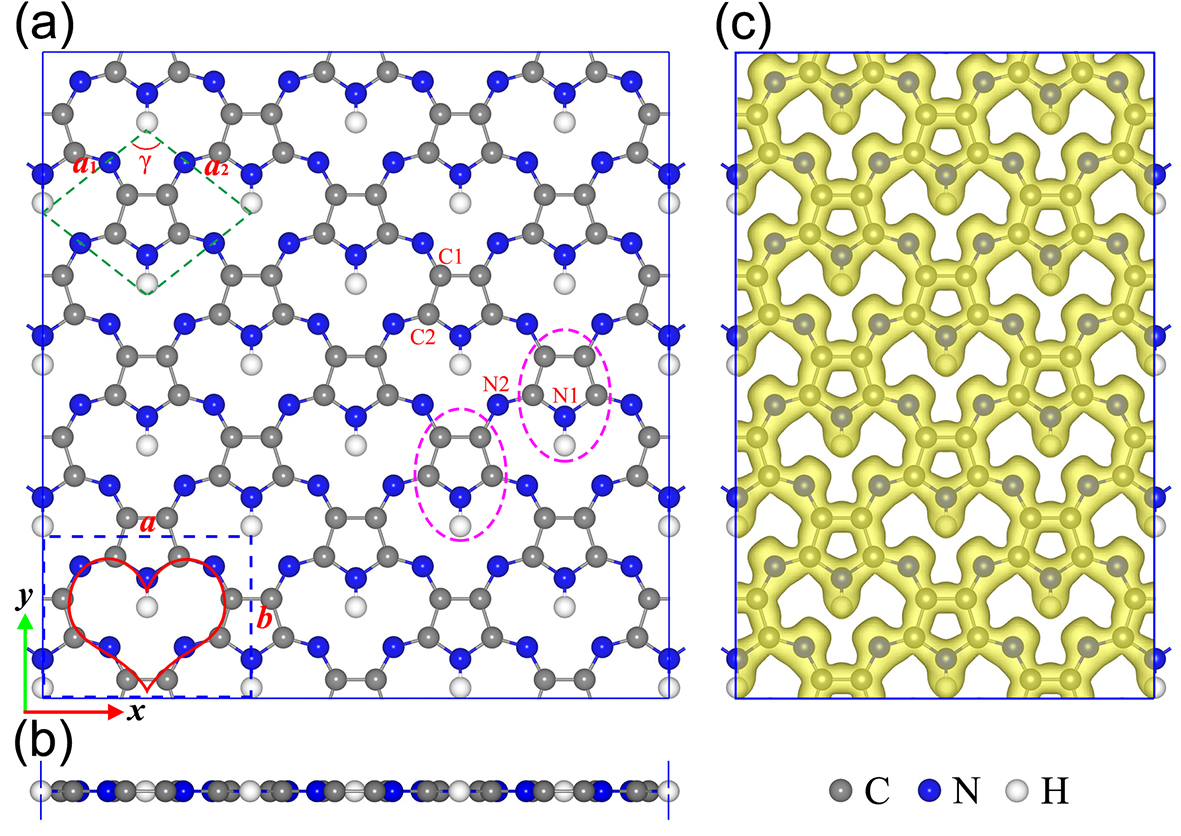
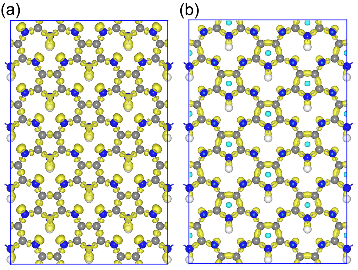
To confirm this conjecture and further elucidate the bonding nature of the C4N3H monolayer, we then calculated the ELF to analyze its electron distributions. As known, ELF can be described in the form of isosurface in real space with isovalues ranging from 0 to 1. The region with 1 indicates the strong covalent electrons or lone-pair electrons, the region close to 0 implies the area with low electron density, and the region with an isovalue of 0.5 is an area with homogeneous electron gas. As shown in Fig. 1(c), the electron gas is well distributed and delocalized at the whole region of this monolayer network, which can electronically stabilize the 2D framework. To highlight the in-plane bonding states, we also plotted the isosurface of ELF for this monolayer with an isovalue of 0.8 in Fig. 2(a). It is found that the ELF localization centers clearly locate at the middle of the C–C, C–N and N–H bonds, indicating that the bonds have strong covalent electron states with -like sp2 hybridization. The bonds between C, N and H atoms can also be evidenced by the deformation electronic density of the C4N3H monolayer [Fig. 2(b)]. The deformation electronic density is defined as the total electronic density of this monolayer excluding those of isolated atoms. Clearly, electrons are well localized over the C–C, C–N and N–H bonds, confirming the conclusion obtained from the ELF and the conjecture we proposed above. In addition, the remaining valence electrons of carbon and nitrogen atoms form the delocalized network, like the case of graphene. According to the Bader charge analysis 34 ; 35 , C1, C2, N1, N2 and H atoms in the C4N3H monolayer respectively possess , , , and charge. This level of charge transfer between C and N atoms is similar to that in stable C2N-h2D monolayer which has been successfully synthesized 22 ; 36 , suggesting that the C4N3H monolayer is likely to have the similar stability.
III.2 Stability of the C4N3H monolayer
To evaluate the feasibility of experimental synthesis and the stability of the C4N3H monolayer, we first calculated its cohesive energy () defined by , where , , and are the calculated total energies of isolated C, N and H atoms, and C4N3H monolayer, respectively; , and are the number of C, N and H atoms in the supercell of this monolayer, respectively. According to our computations, the cohesive energy is 7.88 eV per atom. This value is evidently larger than that of the already-synthesized borophene (5.87 eV per atom) 37 , silicene (4.01 eV per atom) 38 and phosphorene (4.67 eV per atom) 39 , implying the high stability and synthetic feasibility of the C4N3H monolayer from the viewpoint of energy level.
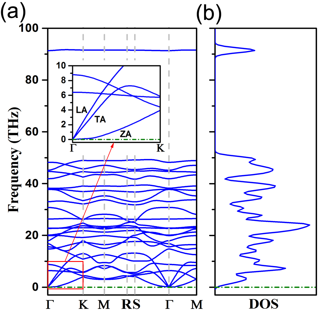
The stability of this monolayer can be further confirmed by its phonon dispersion curves and phonon DOS. As shown in Fig. 3(a), there is no sign of imaginary phonon mode in the phonon spectrum along the highly symmetric points in the entire Brillouin zone. In detail, there are eight atoms in the primitive cell of the C4N3H monolayer, thus its phonon spectrum has twenty-four phonon bands, including three acoustic branches and twenty-one optical branches. The three acoustic branches are respectively transverse acoustic (TA) and longitudinal acoustic (LA) branches corresponding to vibration within the plane, and the other one (ZA) corresponding to vibration out of plane [inset of Fig. 3(a)]. It can be seen that in contrast to the linear dispersion for the TA and LA branches, the frequency of the ZA branch shows a quadratic dispersion near the point. It is worth mentioning that this type of quadratic dispersion of ZA branch is a characteristic feature of the phonon dispersion curves in monolayered or layered crystals, e.g., graphene 40 , graphite 41 and other layered compounds 15 ; 42 ; 43 . As shown in Fig. 3(b), the total phonon DOS also reveals that no phonon with imaginary frequency is found in this monolayer, which agrees very well with its phonon spectrum. These results demonstrate the good dynamic stability of the C4N3H monolayer.
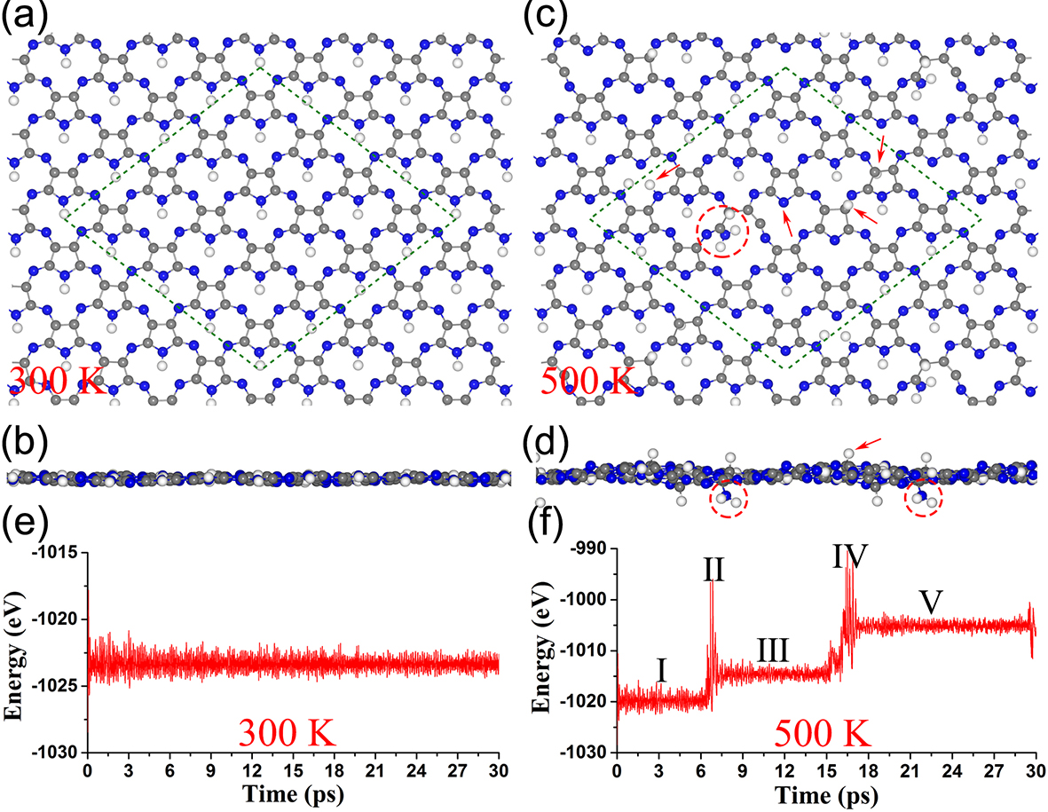
Moreover, to further evaluate the thermal stability of the C4N3H monolayer, we performed FPMD simulations using a supercell containing 64 C atoms, 48 N atoms and 16 H atoms. The initial configuration was annealed at different temperatures of 300, 500 and 1000 K with a time step of 2 fs. As shown in Figs. 4(a) and 4(b), the snapshots of the geometry structure at the end of 30 ps simulations clearly reveal that the C4N3H monolayer can maintain its structural integrity except for some thermal fluctuations at the temperature of 300 K. The total energy of the simulated system can reach equilibrium quickly at 300 K [see Fig. 4(e)], verifying the above result from the viewpoint of energy level. This result can be understood by the fact that the binding energies of the C–C, C–N and C–H bonds are larger than the thermal energy corresponding to room temperature, consistent with other 2D carbon nitride systems 21 ; 22 ; 23 ; 44 . Moreover, this slightly distorted structure can restore its initial planar configuration after complete atomic relaxation.
The structure of this monolayer after annealing at 500 K is shown in Figs. 4(c) and 4(d). Obviously, significant atomic rearrangement took place and the basal plane substantially disordered after thermal annealing [see the partial structures pointed by the red arrows and circles in Figs. 4(c) and 4(d)]. Further analysis of the FPMD simulations reveals the process of the structure collapse at this temperature , as shown in Fig. 4(f) and Fig. 2 of the Supplemental Material 33 . Moreover, this monolayer immediately and completely collapsed at a higher temperature of 1000 K. Hence, combined with the above result that the C4N3H monolayer can maintain its structural integrity at room temperature, we can get the conclusion that this monolayer has a melting point between 300 and 500 K, revealing its decent thermal stability.
Considering the importance of the mechanical stability of a material for its applications, we also studied the mechanical properties of this organic monolayer by examining its elastic constants. It is known that there are four nonzero elastic constants for a 2D material, which are , , () and , respectively. These elastic constants need to satisfy the criteria () for a mechanically stable 2D sheet 45 ; 46 . The in-plane Young s modules along a () and b () directions can be expressed as and . The elastic constants of the C4N3H monolayer computed are = 209.8 N m-1, = 138.7 N m-1, = = 71.5 N m-1 and = 86.0 N m-1. Clearly, these elastic constants satisfy the above criteria, denoting the good mechanical stability of this monolayer. Accordingly, and calculated respectively are 173.1 and 114.3 N m-1, indicating that the C4N3H monolayer is mechanically anisotropic. The Young s modules of this monolayer are higher than those of already-synthesized phosphorene ( = 25.5 N m-1 and = 91.6 N m-1) 39 ; 46 , suggesting its good mechanical property.
Considering that the C4N3H monolayer has comparable cohesive energy to other already-synthesized 2D materials, and dynamic, thermal and mechanical stabilities, we believe that it is viable for its experimental synthesis. It is well known that the condensation reaction is a valid method for producing exotic materials in polymer chemistry. Most importantly, recent developments in this field have already successfully synthesized a series of polymer materials, for instance, g-C3N4 20 ; 21 , C2N-h2D 22 , C3N sheets 23 , 2D COFs 47 ; 48 , metal-organic frameworks 49 , etc. These materials show the tremendous capability of modern chemistry to create novel 2D networks from custom-designed monomers. Inspired by this, we proposed two hypothetical routes to synthesize the C4N3H monolayer based on pyrrole molecules. Firstly, one should respectively nitride (or oxidize) pyrrole molecules to the certain products, and then, 2D C4N3H material can be synthesized via the condensation reaction of these intermediate products (see Fig. 3 of the Supplemental Material 33 ). Herein, it should be noted that the real synthetic process must be much more complicated and difficult. However, it is worth expecting for the experimental realization of this novel material due to its unique electronic properties revealed in the next section.
III.3 Electronic structures of the C4N3H monolayer
As a novel material with intriguing structure, its detailed electronic structure needs to be explored. Thus, we calculated the band structure, total DOS (TDOS) and projected DOS (PDOS) of the C4N3H monolayer. As shown in Fig. 5(a), one can see that this monolayer is a semimetal with the valence and conduction bands meeting in a single point at the Fermi level. The characteristics of linear bands and degenerate state at this point denote the appearance of Dirac states in the C4N3H monolayer. Different from the well-known graphene where Dirac points locate at the high-symmetry points (K and K points), the Dirac point of the C4N3H monolayer locates on the path from the to K point. As a result, there are two symmetry-related Dirac points appearing in the entire first Brillouin zone [only one representative is shown in Figs. 5(a) and 5(c), as the two Dirac points are related by symmetry]. Consistently, its TDOS is zero at the Fermi level [Fig. 5(b)], supporting the presence of the Dirac point. Figure 5(c) shows the first Brillouin zone of the C4N3H monolayer with orthorhombic (Amm2) structure, and further demonstrates that neither honeycomb structure nor hexagonal symmetry is prerequisite for the existence of Dirac cones.
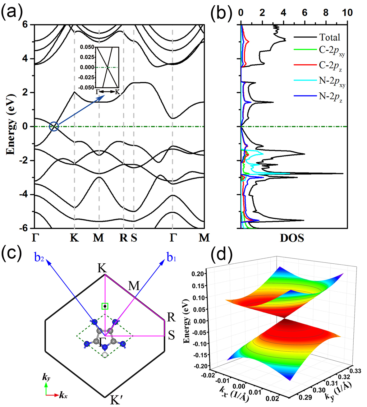
To obtain deeper insight into the Dirac states of this organic monolayer, we further calculated the Dirac cone formed by the valence and conduction bands in the vicinity of the Dirac point. As shown in Fig. 5(d), its Dirac cone is distinctly distorted, similar to that of some inorganic Dirac materials such as phagraphene 13 , 6, 6, 12-graphyne 10 and Pmmn-boronene 12 . The linear dispersion curves of energy and momentum in both the kx and ky directions around the Dirac point suggest the zero effective mass of the carriers (electrons and holes) near the Fermi level. To examine the carrier mobility around the distorted Dirac cone, we then calculated the Fermi velocity () of the C4N3H monolayer using the formula of , where is the slop of valence or conduction band near the Dirac point and is the reduced Plancks constant. The slope of the bands in the kx direction is 7.3 eV Å, equivalent to a Fermi velocity m s-1, while in the ky direction, the slop of the bands equal to 6.2 eV Å ( m s-1) and -2.8 eV Å ( m s-1)(see Fig. 4 of the Supplemental Material 33 ). The largest Fermi velocity is comparable to that in graphene and other 2D inorganic Dirac materials 10 ; 12 ; 13 ; 14 ; 15 , and is roughly one order of magnitude larger than that in 2D organic Dirac materials ever reported 17 ; 18 . It is noted that Fermi velocities in 2D organic polymers followed an approximately inverse exponential relation to their pore size, largely independent of the interconnecting oligomer 18 . That is to say, the 2D organic Dirac polymer with the small pore size is favorable to the high Fermi velocity. Thus, the high Fermi velocity of our organic monolayer may attribute to its angstrom-scale pores. In addition, the anisotropy of the distorted Dirac cone with different slopes at the Dirac point in the kx and ky directions implies the direction-dependent electronic properties of the C4N3H monolayer, indicating its more flexible applications in contrast with graphene.
Additionally, the hybrid HSE06 functional 29 and the SOC effect were respectively used to recalculate the band structure of the C4N3H monolayer for further confirming its Dirac states. As shown in Fig. 5(a) of the Supplemental Material 33 , the dispersion of the valence and conduction bands at the Fermi level given by the HSE06 functional is very similar to that computed based on the PBE functional 25 and no band gap can be identified, indicating that the above predicted intrinsic Dirac states in the C4N3H monolayer still survive to the hybrid HSE06 functional. On the other hand, we also demonstrate that the SOC effect on the electronic properties of this monolayer is negligible and the Dirac cone is still well preserved, which can be seen in Fig. 5(b) of the Supplemental Material 33 . This is unsurprising due to the fact that C, N and H are all light elements, and the SOC effect on the nontrivial gap should be very small.
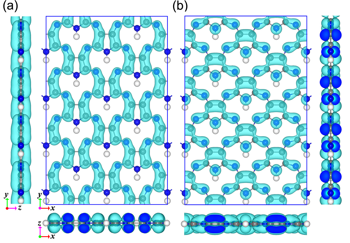
Then, we explored the physical origin of the Dirac states in the C4N3H monolayer. Through analyzing the PDOS of this monolayer [Fig. 5(b)], one can see that both the occupied and unoccupied peaks near the Fermi level mostly originate from the 2pz orbitals of C and N atoms. The calculated orbital-resolved band structures of this monolayer also show the same conclusion that the bands near the Fermi level are mainly contributed by 2pz orbitals of the atoms (see Fig. 6 of the Supplemental Material 33 ). Furthermore, we also calculated the band decomposed charge density at the Dirac point to visualize the above result. Clearly, the electron density distribution presents an obvious characteristic of 2pz orbitals [see the side views of the isosurfaces plotted in Figs. 5(a) and 5(b)]. Moreover, both the top valence band and the bottom of conduction band around the Dirac point are mainly contributed by the 2pz orbitals of C and N2 atoms, while the 2pz orbital of N1 atoms also makes a contribution to the lowest conduction band. These 2pz orbitals overlap, resulting in the formation of an extended -electron conjugation system in the C4N3H monolayer, similar to that in graphene. Accordingly, we can take the conclusion that this -electron conjugation system is the reason for the emergence of Dirac states in this organic monolayer.
IV Conclusion
To summarize, we designed a novel 2D organic material with evenly distributed heart-shaped angstrom-scale pores, namely the C4N3H monolayer. In its unique structure, every C atom is bonded with three other atoms (C or N atoms) via sp2 hybridization, giving rise to three -like orbitals placed in its basal plane and one orbital along Z axis in the perpendicular direction. These and bonds are responsible for the energy stability of the 2D C4N3H framework. Furthermore, we have confirmed its dynamic, thermal and mechanical stabilities respectively by its phonon dispersion curves, FPMD simulations and mechanical properties. Band structure and TDOS clearly reveal that this organic monolayer is a semimetal with anisotropic Dirac cones and very high Fermi velocity which is roughly one order of magnitude larger than that in 2D organic Dirac materials ever reported 17 ; 18 . Based on the PDOS and the band decomposed charge density of this monolayer, we demonstrate that the anisotropic Dirac cones originate from the extended -electron conjugation system which is mainly contributed by the 2pz orbitals of C and N atoms. These results indicate that we successfully designed a 2D organic Dirac material with high Fermi velocity which can be comparable to that in 2D inorganic ones. We hope that our findings will promote the experimental realization of this novel material and greatly push forward the study of the 2D organic Dirac materials.
Acknowledgements.
We thank Feng Liu of University of Utah for helpful discussion. This work was financially supported by the State Key Program for Basic Research (Grant Nos. 2014CB921102 and 2017YFA0206304) and NSFC (Grant Nos. 51572122 and 11304096), China. We are grateful to the High Performance Computing Center of Nanjing University for doing the numerical calculations in this paper on its blade cluster system.References
- (1) A. H. Castro Neto, F. Guinea, N. M. R. Peres, K. S. Novoselov, and A. K. Geim, Rev. Mod. Phys. 81, 109 (2009).
- (2) J. E. Moore, Nature 464, 194 (2010).
- (3) T. O.Wehling, A. M. Black-Schaffer, and A. V. Balatsky, Adv. Phys. 63, 1 (2014).
- (4) K. S. Novoselov, A. K. Geim, S. V. Morozov, D. Jiang, M. I. Katsnelson, I. V. Grigorieva, S. V. Dubonos, and A. A. Firsov, Nature 438, 197 (2005).
- (5) M. I. Katsnelson, K. S. Novoselov, and A. K. Geim, Nat. phys. 2, 620 (2006).
- (6) C. R. Dean, L.Wang, P. Maher, C. Forsythe, F. Ghahari, Y. Gao, J. Katoch, M. Ishigami, P. Moon, M. Koshino, T. Taniguchi, K.Watanabe, K. L. Shepard, J. Hone, and P. Kim, Nature 497, 598 (2013).
- (7) R. Yu, W. Zhang, H.-J. Zhang, S.-C. Zhang, X. Dai, and Z. Fang, Science 329, 61 (2010).
- (8) K. Asano and C. Hotta, Phys. Rev. B 83, 245125 (2011).
- (9) J. Wang, S. Deng, Z. Liu, and Z. Liu, Natl. Sci. Rev. 2, 22 (2015).
- (10) D. Malko, C. Neiss, F. Viñes, and A. Görling, Phys. Rev. Lett. 108, 086804 (2012).
- (11) W. Li, M. Guo, G. Zhang, and Y.-W. Zhang, Phys. Rev. B 89, 205402 (2014).
- (12) X.-F. Zhou, X. Dong, A. R. Oganov, Q. Zhu, Y. Tian, and H.-T. Wang, Phys. Rev. Lett. 112, 085502 (2014).
- (13) Z. Wang, X.-F. Zhou, X. Zhang, Q. Zhu, H. Dong, M. Zhao, and A. R. Oganov, Nano Lett. 15, 6182 (2015).
- (14) S. Cahangirov, M. Topsakal, E. Aktürk, H. Şahin, and S. Ciraci, Phys. Rev. Lett. 102, 236804 (2009).
- (15) H. Zhang, Y. Li, J. Hou, A. Du, and Z. Chen, Nano Lett. 16, 6124 (2016).
- (16) M. O. Goerbig, J.-N. Fuchs, G. Montambaux, and F. Piéchon, Phys. Rev. B 78, 045415 (2008).
- (17) M. Hirata, K. Ishikawa, K. Miyagawa, M. Tamura, C. Berthier, D. Basko, A. Kobayashi, G. Matsuno, and K. Kanoda, Nat. Commun. 7, 12666 (2016).
- (18) J.-J. Adjizian, P. Briddon, B. Humbert, J.-L. Duvail, P. Wagner, C. Adda, and C. Ewels, Nat. Commun. 5, 5842 (2014).
- (19) K. Medjanik, O. Fedchenko, S. Chernov, D. Kutnyakhov, M. Ellguth, A. Oelsner, B. Schönhense, T. R. F. Peixoto, P. Lutz, C.-H. Min, F. Reinert, S. Däster, Y. Acremann, J. Viefhaus, W. Wurth, H. J. Elmers, and G. Schönhense, Nat. Mater. 16, 615 (2017).
- (20) X. Wang, K. Maeda, A. Thomas, K. Takanabe, G. Xin, J. M. Carlsson, K. Domen, and M. Antonietti, Nat. Mater. 8, 76 (2009).
- (21) G. Algara-Siller, N. Severin, S. Y. Chong, T. Björkman, R. G. Palgrave, A. Laybourn, M. Antonietti, Y. Z. Khimyak, A. V. Krasheninnikov, J. P. Rabe, U. Kaiser, A. I. Cooper, A. Thomas, and M. J. Bojdys, Angew. Chem. Int. Ed. 53, 7450 (2014).
- (22) J. Mahmood, E. K. Lee, M. Jung, D. Shin, I.-Y. Jeon, S.-M. Jung, H.-J. Choi, J.-M. Seo, S.-Y. Bae, S.-D. Sohn, N. Park, J. H. Oh, H.-J. Shin, and J.-B. Baek, Nat. Commun. 6, 6486 (2015).
- (23) S. Yang, W. Li, C. Ye, G. Wang, H. Tian, C. Zhu, P. He, G. Ding, X. Xie, Y. Liu, Y. Lifshitz, S.-T. Lee, Z. Kang, and M. Jiang, Adv. Mater. 29, 1605625 (2017).
- (24) A. Savin, R. Nesper, S. Wengert, and T. F. Fässler, Angew. Chem. Int. Ed. 36, 1808 (1997).
- (25) J. P. Perdew, K. Burke, and M. Ernzerhof, Phys. Rev. Lett. 77, 3865 (1996).
- (26) D. Vanderbilt, Phys. Rev. B 41, 7892 (1990).
- (27) G. Kresse and J. Furthmüller, Phys. Rev. B 54, 11169 (1996).
- (28) P. E. Blöchl, Phys. Rev. B 50, 17953 (1994).
- (29) J. Heyd, G. E. Scuseria, and M. Ernzerhof, J. Chem. Phys. 124, 219906 (2006).
- (30) A. Togo, F. Oba, and I. Tanaka, Phys. Rev. B 78, 134106 (2008).
- (31) S. Nosé, Mol. Phys. 52, 255 (1984).
- (32) D. W. Boukhvalov, M. I. Katsnelson, and A. I. Lichtenstein, Phys. Rev. B 77, 035427 (2008).
- (33) See Supplemental Material at http://link.aps.org/supplemental/XXX for details on geometric structure, stability and electronic structures of the C4N3H monolayer.
- (34) G. Henkelman, A. Arnaldsson, and H. Jónsson, Comp. Mater. Sci. 36, 354 (2006).
- (35) E. Sanville, S. D. Kenny, R. Smith, and G. Henkelman, J. Comput. Chem. 28, 899 (2007).
- (36) J. Kang, S. Horzum, and F. M. Peeters, Phys. Rev. B 92, 195419 (2015).
- (37) A. J. Mannix, X.-F. Zhou, B. Kiraly, J. D. Wood, D. Alducin, B. D. Myers, X. Liu, B. L. Fisher, U. Santiago, J. R. Guest, M. J. Yacaman, A. Ponce, A. R. Oganov, M. C. Hersam, and N. P. Guisinger, Science 350, 1513 (2015).
- (38) A. Fleurence, R. Friedlein, T. Ozaki, H. Kawai, Y.Wang, and Y. Yamada-Takamura, Phys. Rev. Lett. 108, 245501 (2012).
- (39) L. Li, Y. Yu, G. J. Ye, Q. Ge, X. Ou, H. Wu, D. Feng, X. H. Chen, and Y. Zhang, Nat. Nanotechnol. 9, 372 (2014).
- (40) J.-A. Yan, W. Y. Ruan, and M. Y. Chou, Phys. Rev. B 77, 125401 (2008).
- (41) N. Mounet and N. Marzari, Phys. Rev. B 71, 205214 (2005).
- (42) H. Pan, Y. Sun, Y. Zheng, N. Tang, and Y. Du, New J. Phys. 18, 093021 (2016).
- (43) H. Zabel, J. Phys.: Condens. Matter 13, 7679 (2001).
- (44) A. Du, S. Sanvito, and S. C. Smith, Phys. Rev. Lett. 108, 197207 (2012).
- (45) S. Zhang, J. Zhou, Q. Wang, X. Chen, Y. Kawazoe, and P. Jena, Proc. Natl Acad. Sci. USA 112, 2372 (2015).
- (46) Y. Wang, F. Li, Y. Li, and Z. Chen, Nat. Commun. 7, 11488 (2016).
- (47) C. S. Diercks and O. M. Yaghi, Science 355, 923 (2017).
- (48) J. W. Colson, A. R.Woll, A. Mukherjee, M. P. Levendorf, E. L. Spitler, V. B. Shields, M. G. Spencer, J. Park, and W. R. Dichtel, Science 332, 228 (2011).
- (49) T. Kambe, R. Sakamoto, K. Hoshiko, K. Takada, M. Miyachi, J.-H. Ryu, S. Sasaki, J. Kim, K. Nakazato, M. Takata, and H. Nishihara, J. Am. Chem. Soc. 135, 2462 (2013).