Time resolved photoemission spectroscopy of electronic cooling and localization in CH3NH3PbI3 crystals
Abstract
We measure the surface of CH3NH3PbI3 single crystals by making use of two photon photoemission spectroscopy. Our method monitors the electronic distribution of photoexcited electrons, explicitly discriminating the initial thermalization from slower dynamical processes. The reported results disclose the fast dissipation channels of hot carriers (0.25 ps), set a upper bound to the surface induced recombination velocity ( cm/s) and reveal the dramatic effect of shallow traps on the electrons dynamics. The picosecond localization of excited electrons in degraded CH3NH3PbI3 samples is consistent with the progressive reduction of photoconversion efficiency in operating devices. Minimizing the density of shallow traps and solving the aging problem may boost the macroscopic efficiency of solar cells to the theoretical limit.
I Introduction
Hybrid metal-organic perovskite semiconductors such as methylammonium lead iodide CH3NH3PbI3 (MAPbI3) have emerged as promising new materials for photovoltaic devices and optoelectronics. The power conversion efficiency of solar cells based on perovskite materials exceeded 20% within eight years Zhou ; Yang ; Table and a theoretical limit of 30% has been proposed Wei . Such an impressive performance results from favorable material properties such as direct band gap of roughly 1.6 eV, large absorption coefficient and high charge carriers mobility Brenner .
The perovskite materials can be broadly divided into two types: bulk crystals and polycrystalline thin films. Single crystals of MAPbI3, have long electron-hole diffusion length (up to 175 m) and low density of recombination centers Cao ; Valverde ; Tian . Thin films are more suitable for device application but display photoexcited carriers with smaller mobility and shorter lifetime Ponseca ; Herz_Reco ; Herz_Moby . Moreover, the fast degradation of thin films in operating conditions poses serious limits to viable applications. Both the photoexposure and annealing in atmospheric conditions induces the formation of PbI2 inclusionsJemli . The main objective of our work is to show that compositional disorder leads to shallow traps where carriers localize on the picosecond timescale.
The carriers diffusion, localization and recombination is investigated by Two Photon PhotoEmission (2PPE) experiments on single MAPbI3 crystals. Remarkably, 2PPE monitors the energy distribution of excited electrons with good temporal resolution and high surface sensitivity. Moreover, the clean surface of a single crystal is a model and well controlled system where to explore the impact of localized states on the electronic motion.
The article is organized as follow: Section II contains X-rays diffraction, photoluminescence and photoemission characterization of our crystals. Section III describes the methodology and the technical aspects of the 2PPE technique. Section IV discusses the subpicosecond cooling of excited electrons. Section V proposes a diffusion model to explain the observed evolution of 2PPE signal. Section VI investigates the carriers localization in intentionally degraded crystals. Section VII deals with carriers recombination and possible effects of the surface. Section VIII reports the conclusions and acknowledgments.
II Sample characterization
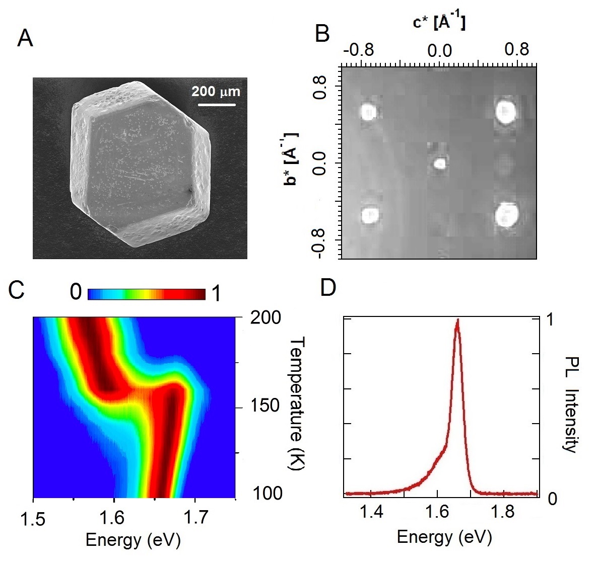
We investigate single crystals of MAPbI3 grown by inverse crystallization method. Methylammonium iodide (0.78 g, 5 mmol) and lead iodide (2.30 g, 5 mmol) were dissolved in gamma-butyrolactone (5 mL) at 60 ∘C. The yellow solution (2 mL) was placed in a vial and heated at 120 ∘C during one to four hours depending on the desired crystal size. As shown in the scanning electron microscope image of Fig. 1A, the samples are crystals of millimetric size. X-ray diffraction measurents have been performed at the CRISTAL beamline of synchrotron SOLEIL by means of a four-circle diffractometer. The Bragg’s reflections in Fig. 1B confirm the high quality of the single crystals Antonio .
Figure 1C displays the photoluminescence map of the MAPbI3 single crystals between 100 K and 200 K. The emission is composed of a single peak arising from electron-hole recombination across the band-gap. Upon cooling, the sudden blueshift of the emission line at K Deleporte is due to the widening of band gap at the tetragonal to orthorhombic phase transition. Below 160 K, the evolution of photoluminescence with temperature indicates a reduction of the band gap with lattice contraction. From the photoluminescence spectrum recorded at 130 K (see Fig. 1D), we extract the band gap energy eV. In the following, we will refer all spectroscopic measurements to the orthorhombic phase at 130 K.
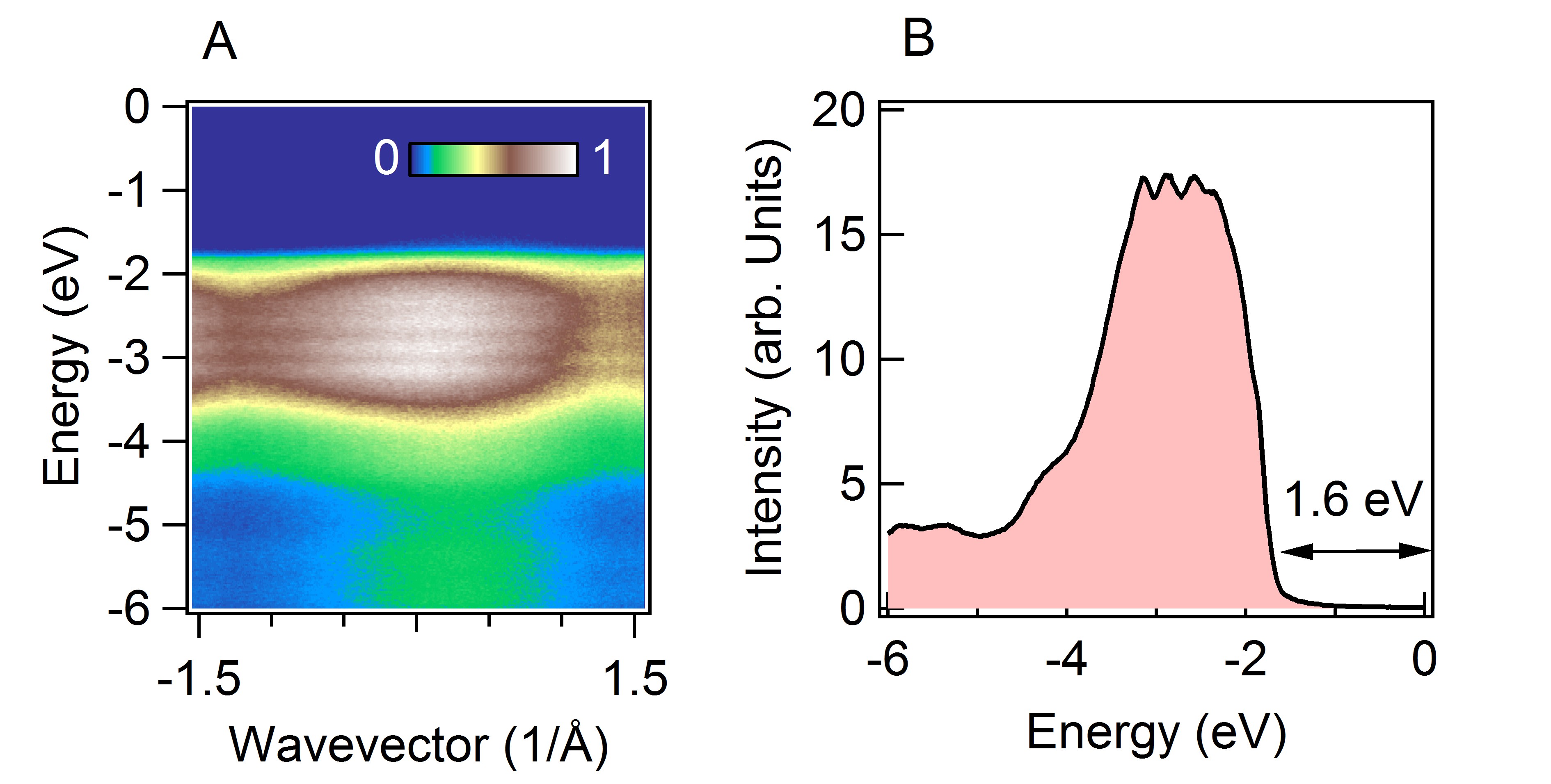
Single crytals have been mounted on the {0,1,0} plane and cleaved in ultra high vacuum at base pressure below 10-10 mbar. Despite the high crystalline quality of our samples, Low Energy Electron Diffraction (LEED) did not display any Bragg spot. We evince that cleaved surfaces are rough, probably because of the brittle nature of MAPbI3. Figure 2A shows Angle Resolved PhotoElectron Spectroscopy (ARPES) measurements performed at the CASSIOPEE beamline of synchrotron SOLEIL. The selected photon beam of 94 eV maximizes the cross section of the valence band and corresponds to a perpendicular wavevector . Variations of spectral intensity with respect to are consistent with the electronic band dispersion in the first Brillouin zone Antonio . We show in Fig. 2B the spectrum obtained by integrating the photoelectron map in the interval [-1.5,1.5] Å-1. The chemical potential is located 1.6 eV higher than the top of the valence band, indicating that MAPbI3 crystals are naturally -doped.
III Two Photon PhotoEmission
The temporal evolution of the excited state is measured by means of Two Photon PhotoEmission (2PPE). Our photon source is a Ti:Sapphire laser system delivering 6 J pulses with repetition rate of 250 kHz. Part of the fundamental beam ( eV) is converted to the second harmonic ( eV) in a -BBO crystal while the rest is employed to generate the third harmonic ( eV) Faure . We photoexcite the sample at 130 K by 50 fs pump pulses of 20 J/cm2, centered at . According to the reported value of the absorption coefficient Green , this pulse results in an electron-hole density of cm-3.
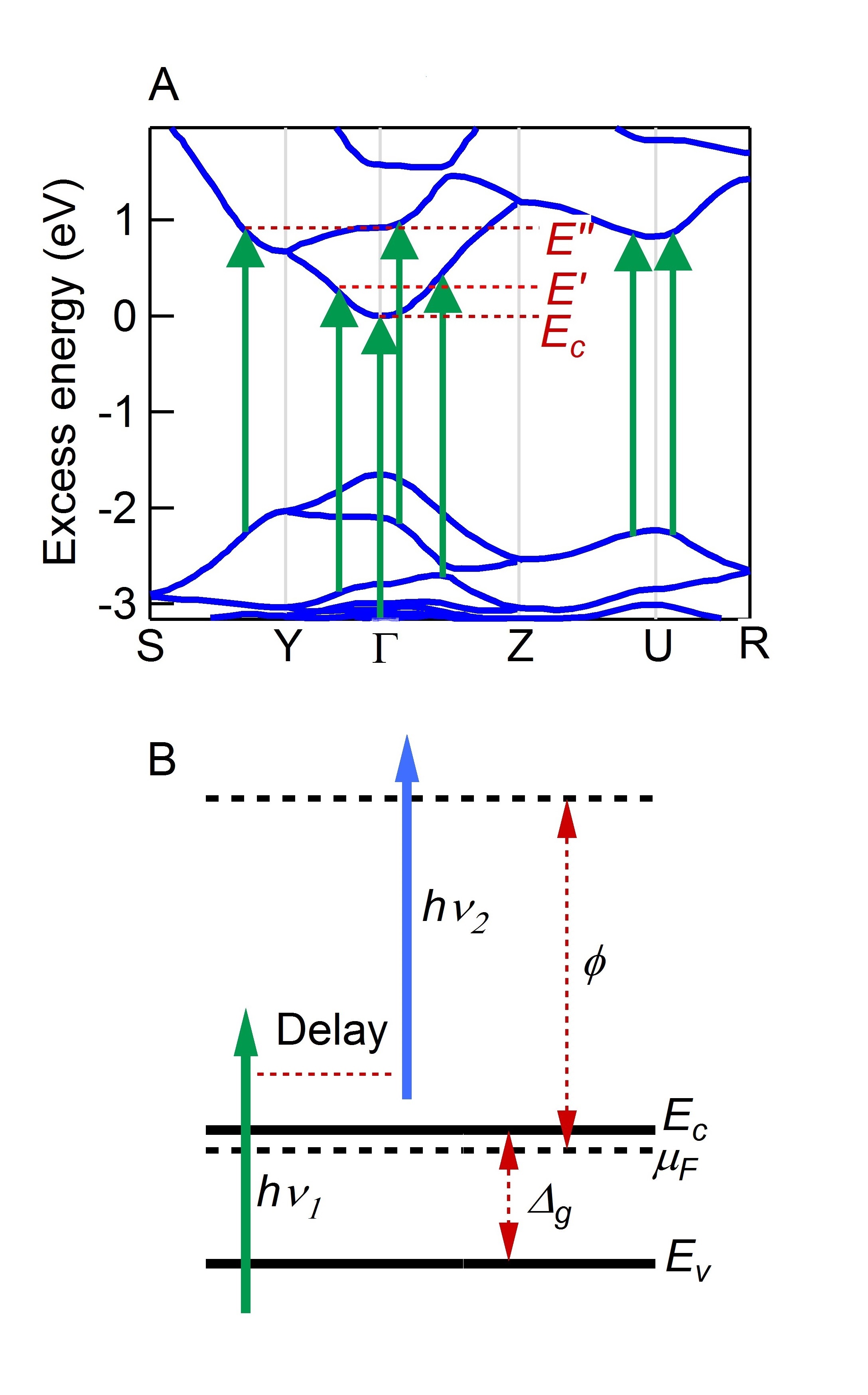
As shown in Fig. 3A the photons of the pump beam generate photoexcited electrons with excess energy up to eV, thereby inducing optical transitions in two branches of the conduction band. After a variable delay time, probe pulses centered at eV promote the excited electrons above the vacuum level (see Fig. 3B). Photoelectrons outgoing from the sample are detected by a hemispherical energy analyzer with an acceptance angle of roughly degrees2 around normal emission. The overall energy resolution of 60 meV is dominated by the bandwidth of the probe beam. This technique provides a direct mapping of the electronic distribution in the photoexcited sample. Moreover, the electrons that have absorbed the two photons hold an ineastic mean free path of few nanometers Unal . Such high surface sensitivity can be exploited to question the electrons dynamics in the topmost layers of the cleaved crystal.
IV Ultrafast cooling of hot electrons
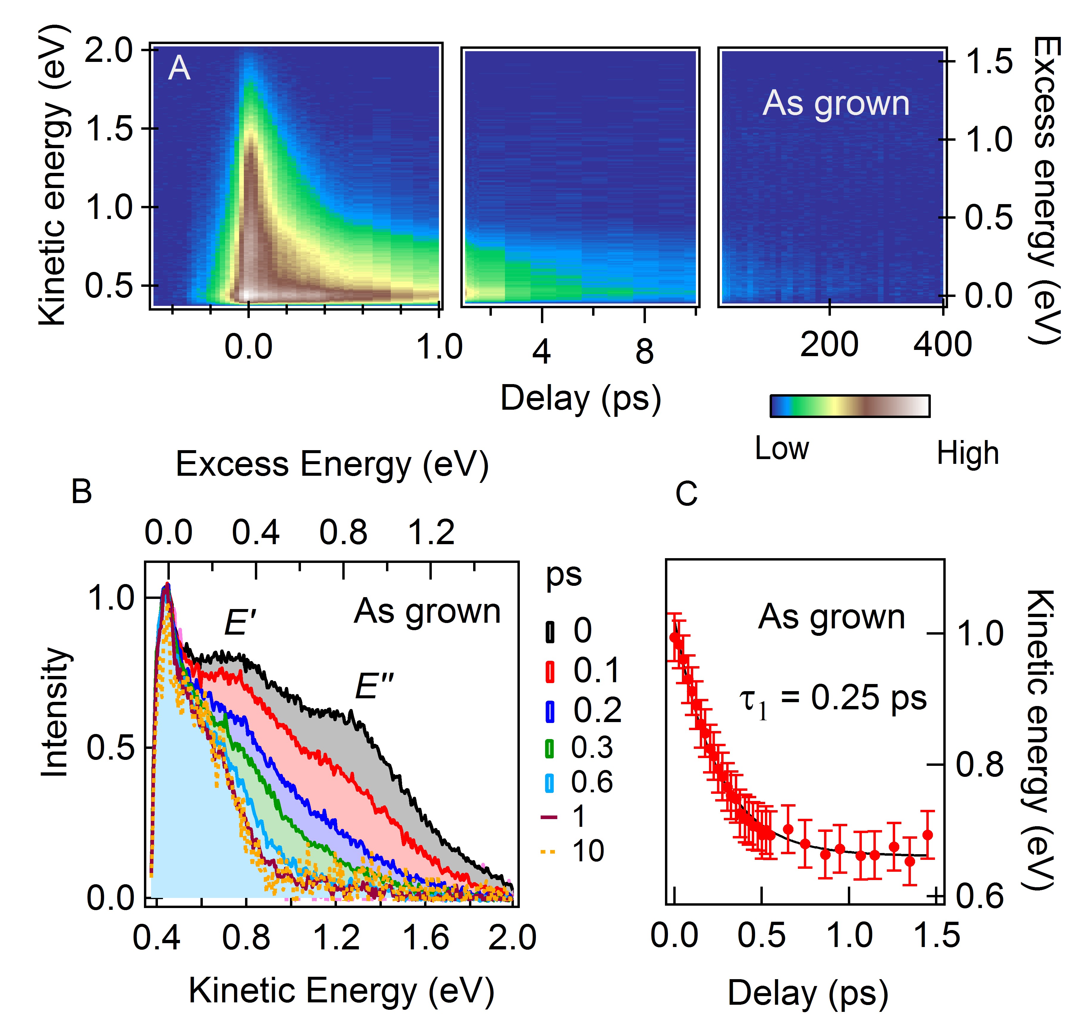
We show in Fig. 4A a color scale plot of the photoelectron intensity acquired as a function of kinetic energy and pump probe delay. The nominal kinetic energy of the conduction band minimum is eV, where eV is the workfunction of our analyzer. As shown in Fig. 4B, the spectrum acquired at the maximal overlap between pump and probe pulse (zero delay) displays a peak in proximity of , a second peak near to eV and a third peak at eV. As sketched in Fig. 3A, the structures and are located at excess energies where the 3.15 eV photons generate high density of optical transitions Filip .
Next, we consider the dynamics of the electrons soon after the arrival of the pump pulse. Figure 4B shows that the excited electronic distribution varies strongly within the first picosecond. The electrons with large excess energy thermalize towards the bottom of the conduction band by means of electron-electron scattering and phonon emission. We exclude the occurrence of carriers multiplication because the photon energy of the pump beam is lower than twice the value of the bandgap. The initial thermalization time can be quantified by evaluating the average kinetic energy contained in the spectrum as a function of time. In practice, we calculate , where is the kinetic energy, is the photoelectron intensity, and is the pump-probe delay.
Figure 4C shows the resulting together with the fit by an exponential decay with time constant of ps. This value is in excellent agreement with recent 2PPE experiments on MAPbI3 thin films Niesner and it is faster than the energy relaxation time observed in inorganic semiconductors Tanimura . We suggest that the rapid electronic cooling of MAPbI3 arises via the coupling of excited carriers to the internal vibrations of the CH3NH cations. For example, the stretching modes of C-H and N-H bonds holds quantum energy of meV and can efficiently drain the excess energy of photoexcited electrons Brivio . Moreover, the recent observation of optical sidebands in two-dimensional hybrid perovskites indicate a sizable coupling of the exciton to an organic mode with quantum energy of 40 meV Straus .
According to Fig. 4C, the hot electrons will reach quasi-equilibrium with the coupled phonons after ps. Several authors suggested that strongly coupled modes attain an occupation level higher than the thermal one and relax on the slower timescale of anharmonic interaction Beard_hot ; Price . In this respect, time resolved Raman experiments may be helpful to address the specific vibrational modes where electrons transfer their excess energy Heinz . Note in Fig. 4B that the spectra acquired at delay time of 1 ps and 10 ps display a shoulder at excess energy eV. Niesner et al. observed a similar shoulder only in the tetragonal phase of MAPbI3 and they ascribed it to an unconventional kind of polaronic dressing Niesner ; Zhu . This issue requires additional measurements and it is currently under investigation.
V Diffusion in the as-grown sample
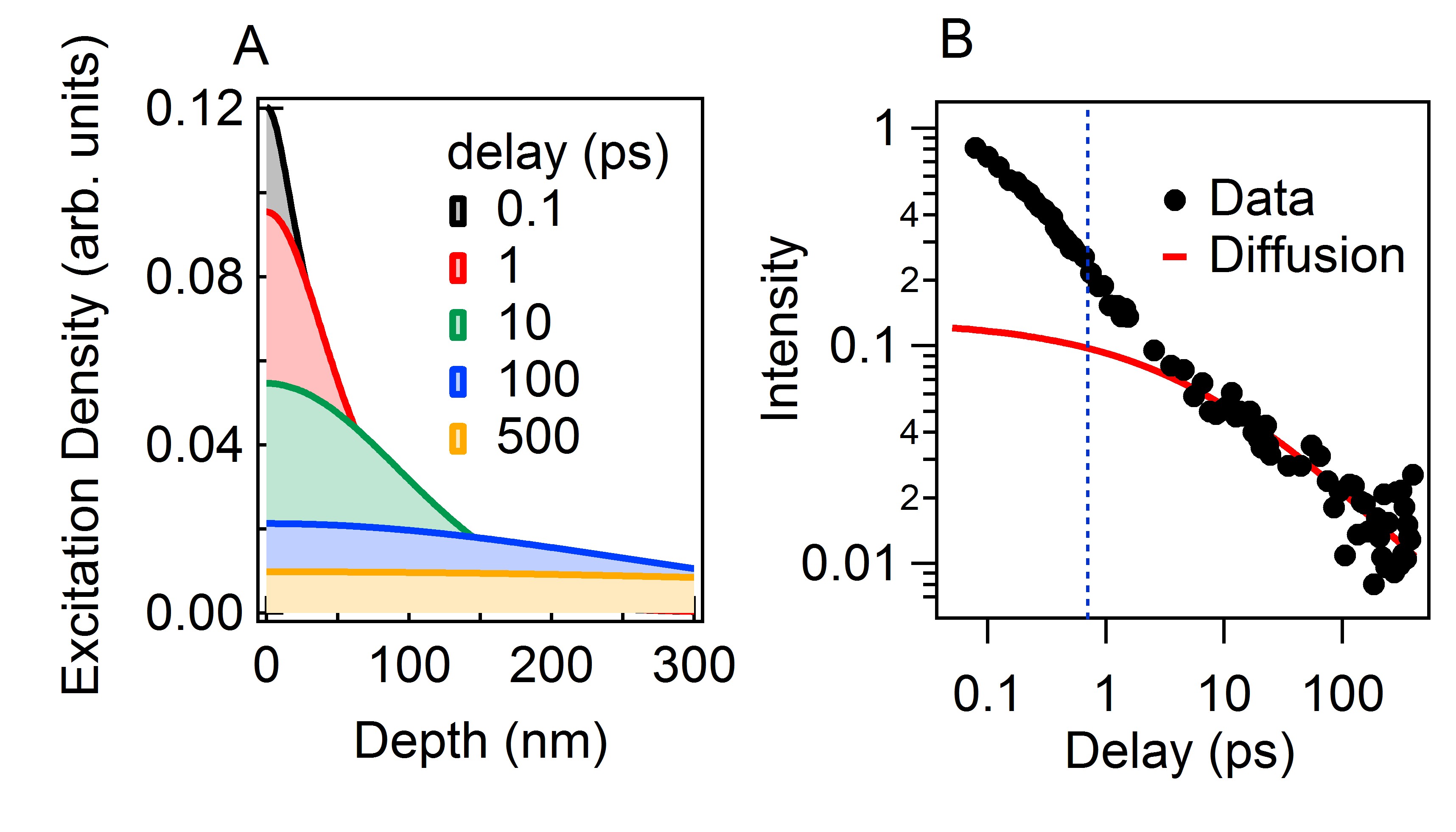
Since the 2PPE technique probes carriers within the topmost nanometers, the integrated signal follows the instantaneous electronic concentration at the surface of the sample times the photoemission cross section. Once the electrons have fully thermalized, the photoemission cross section becomes time independent. Therefore, the progressive decay of 2PPE signal that can be observed in the middle and right panel of Fig. 4A is due to the drift-diffusion of electronic charges from the surface into the bulk. First, we analyze the effect of pure diffusion on the long timescale dynamics. Electrons that are excited in an optical penetration depth Green nm move in to the bulk because of Brownian motion. The electronic concentration at distance from the surface and pump-probe delay is given by Beard_Reco
| (1) |
where and is the electrons diffusion constant of MAPbI3 crystals at 130 K. We recall that the mobility of MAPbI3 is limited by electron-phonon scattering Herz_Moby and scales as . Therefore, we can invoke the Einstein relation and refer to the literature value of at room temperature Cao in order to estimate the electron diffusion constant at T=130 K. The resulting cm2/s is plugged in to equation 1 of the electronic density. We show in Fig. 5A the resulting as a function of for selected values of . Figure 5B compares the calculated with the experimental evolution of the photoemission signal in the temporal window [0.05,400] ps. The measured decay follows the diffusion behavior for delay time larger than 3 ps but proceeds much faster during the first picosecond. Niesner et al. ascribed this initial drop to the rapid variation of the photoemission cross section during the thermalization process Niesner . On one hand, it is fully plausible that carriers changing energy and wavevector display sudden changes of cross section. On the other hand, the measured intensity deviates from the diffusion model even after that the electrons have fully thermalized (namely for ). Eventually, built-in fields at the sample surface lead to an initial drift of the electrons out of the detection regions. Such ultrafast segregation between electrons and holes has been recently observed in other doped semiconductors Hajlaoui . In the case of MAPbI3 the built-in field may originate from the residual polarity of the crystal termination She .
VI Electronic localization in annealed samples
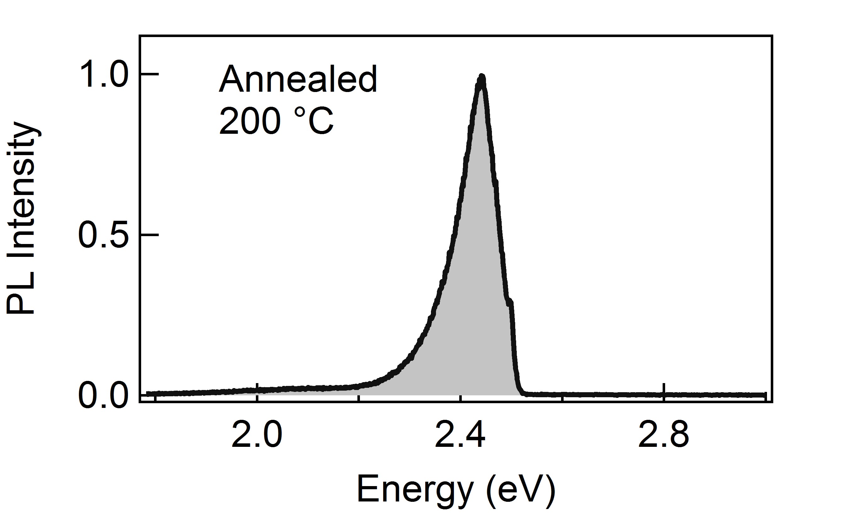
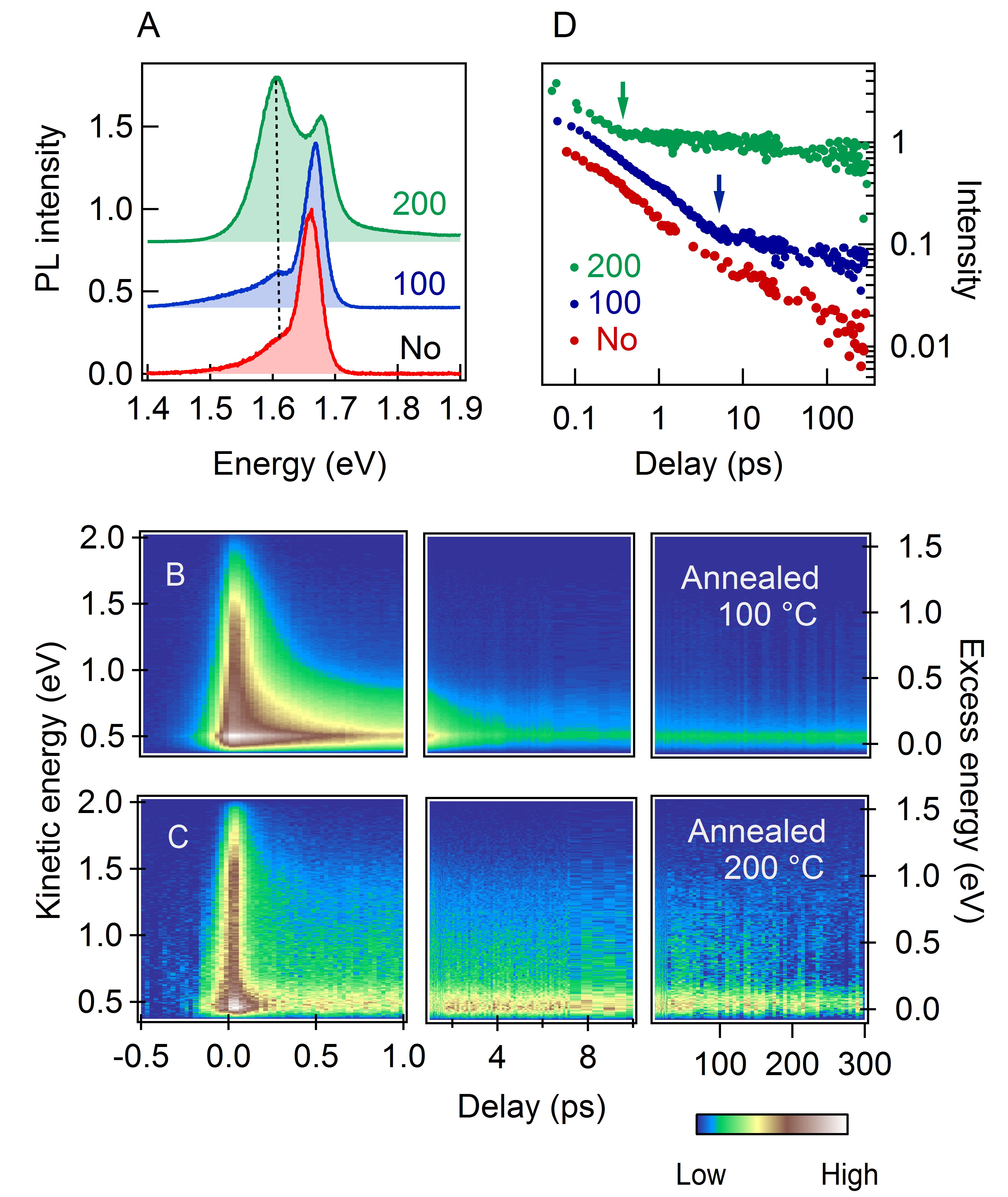
After having discussed the drift-diffusion of the electrons in high quality crystals, we can address the important role that sample degradation has on the carriers motion. The data of the as-grown crystal are compared with the ones of the samples annealed in air at 100 ∘C (MA100) and 200 ∘C (MA200) for 30 minutes. The MAPbI3 single crystal is very sensitive to humidity, illumination and annealing temperature. Figure 6A shows photoluminescence on the as-grown and annealed samples. Upon increasing the annealing temperature, a new photoluminescence peak, arising from trapped states, develops meV below the bandgap value. We report in 6B,C the photoelectron intensity map acquired on annealed samples as a function of pump-probe delay. The MA100 and the as-grown sample display similar behavior on the short timescale ( ps). However the 2PPE map of MA100 (Fig. 6B) and MA200 (Fig. 6C) holds a remnant signal up to 400 ps. We evince that shallow traps introduced by annealing lead to a partial localization of the electrons. Note in Fig. 6D that the long timescale evolution of integrated 2PPE signal deviates from the diffusive decay only in the case of annealed samples. The onset of the trapping strongly depends on the quality of the crystal. In MA100 the localization takes place on the timescale of few picoseconds whereas it falls below the picosecond in highly degraded MA200. Probably the defect density of MA200 is so high that localization takes place as soon as the electrons cool down below the mobility edge of the traps. The localization landscape of conduction electrons is related to the compositional disorder of degraded samples Jemli . According to Xie et al., an annealing to 150 ∘C leads to a shallow distribution of I and Pb components in the MAPbI3 thin film Xie . Furthermore, Deretzis et al. reported that thermodynamic degradation above 150 ∘C can induce a partial conversion of MAPbI3 in to PbI2 Deretzis . The low temperature photoluminescence measurements in Fig. 7 confirms that MA200 contains large inclusions of PbI2.
VII Radiative and surface recombination
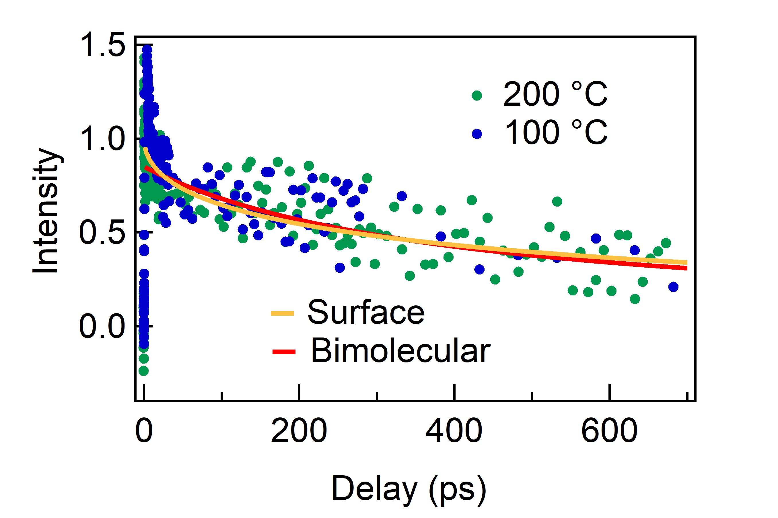
Remarkably, the long lasting presence of electrons at the surface of MA100 and MA200 indicates a long recombination time of the photoexcited carriers. It has been shown that direct recombination between electrons and holes Herz_Reco becomes dominant at photoexcitation density cm-3. We display in Fig. 8 the fitting curve obtained by a kinetic equation with bimolecular recombination rate cm3/s. The extracted value is in good agreement with previous reports and defies the Langevin prediction by four orders of magnitude Herz_Reco . Wehrenfennig et al. proposed that electrons and holes are prefentially localized in spatially distinct regions of the disordered landscape. Accordingly, density functional calculations on MaPbI3 predict that valence band maxima consist of - and orbitals of lead and iodine, respectively, while conduction band minima mostly incorporate orbitals of lead Nakao .
Next, we exploit the high surface sensitivity of 2PPE to question the surface recombination velocity of samples cleaved in ultra high vacuum conditions. By following the literature Beard_Reco ; Hoffman , we model the density of the electrons at the surface as
| (2) |
where is the diffusion constant of trapped electrons and is the velocity of surface recombination. Figure 8 compares the long timescale dynamics measured in the MA100 and MA200 crystals with the fit obtained for cm/s and cm2/s. Such value is strictly an upper bound because: i) we chose the value that provides a good fit and maximize , ii) we implicitly assume that the observed decay is ruled by surface recombination instead of bimolecular recombination. The upper bound of is not far from the surface recombination velocity estimated in other hybrid perovskites Beard_Reco ; Wu . It should be outlined that cm/s is two or three orders of magnitude lower than the surface recombination velocity of most unpassivated semiconductors Schmutten ; Riffe . Accordingly, the electronic structure calculations do not predict mid-gap states at MaPbI3 surfaces with thermodynamical stabilityHaruyama . In operating devices, this asset favors the efficient extraction or injection of carriers at the electrical contacts with the MAPbI3 layer.
VIII Conclusions
To conclude, we characterized the dynamics of excited electrons at the surface of MAPbI3. Our data provide a direct visualization of the electronic cooling at early delay times. It follows that photoexcited carriers thermalize on a subpicosecond timescale, presumably because of the coupling to the vibrations of organic cations. In the as-grown crystal, the electrons dynamics is ruled by diffusion at long timescales. Most likely, an additional drift due to built-in fields sets in at early delay.
We intentionally induce compositional disorder in some MAPbI3 crystals by thermal annealing in atmospheric conditions. As a result, the photoexcited electrons are localized by shallow traps within few picoseconds. Such localization mechanism is consistent with the drop of photoconversion efficiency in aged cells. Finally we estimate the surface recombination velocity of MAPbI3 cleaved in ultra high vacuum. The upper bound obtained by our analysis is consistent with previous results and is several orders of magnitude lower than the values reported in many unpassivated semiconductors.
The project leading to this article has received funding from the European Union’s Horizon 2020 research and innovation program under grant agreement No 687008 (GOTSolar). We also thanks dim-nanoK for funding under project ’PIED’, the DIM-Oximore and the Ecole Polytechnique for funding under the project ’ECOGAN’.
References
- (1) Huanping Zhou, Qi Chen, Gang Li, Song Luo, Tze-bing Song, Hsin-Sheng Duan, Ziruo Hong, Jingbi You, Yongsheng Liu, Yang Yang, Science 345 542 (2014).
- (2) Woon Seok Yang, Jun Hong Noh, Nam Joong Jeon, Young Chan Kim, Seungchan Ryu, Jangwon Seo, Sang Il Seok, Science 348, 1234 (2015).
- (3) Solar cell efficiency tables (version 48), Martin A. Green, Keith Emery, Yoshihiro Hishikawa, Wilhelm Warta Ewan D. Dunlop Prog. Photovolt: Res. Appl. 24 905–913 (2016).
- (4) E. I. Wei, Ren Sha Xingang, Chen Luzhou and C. H. Choy Wallace Appl. Phys. Lett. 106, 221104 (2015).
- (5) Thomas M. Brenner, David A. Egger, Leeor Kronik, Gary Hodes and David Cahen, Nature Reviews Materials 1, 15007 (2016).
- (6) Qingfeng Dong, Yanjun Fang, Yuchuan Shao, Padhraic Mulligan, Jie Qiu, Lei Cao, Jinsong Huang, Science 347 967 (2015).
- (7) David A. Valverde-Chavez, Carlito S. Ponseca, Constantinos C. Stoumpos, Arkady Yartsev, Mercouri G. Kanatzidis, Villy Sundströmb and David G. Cooke, Energy Environ. Sci. 8, 3700 (2015).
- (8) Wenming Tian, Chunyi Zhao, Jing Leng, Rongrong Cui, and Shengye Jin, J. Am. Chem. Soc. 137 12458 (2015).
- (9) Carlito S. Ponseca, Tom J. Savenije, Mohamed Abdellah, Kaibo Zheng, Arkady Yartsev, Tobjörn Pascher, Tobias Harlang, Pavel Chabera, Tonu Pullerits, Andrey Stepanov, Jean-Pierre Wolf, and Villy Sundström, J. Am. Chem. Soc. 136, 5189 (2014).
- (10) Christian Wehrenfennig, Giles E. Eperon, Michael B. Johnston, Henry J. Snaith, Laura M. Herz, Advanced Materials 26, 1584 (2014).
- (11) Perovskite Thin Films, Rebecca L. Milot , Giles E. Eperon , Henry J. Snaith , Michael B. Johnston, and Laura M. Herz, Adv. Funct. Mater. 25, 6218 (2015).
- (12) Khaoula Jemli, Hiba Diab, Ferdinand Lédée, Gaelle Trippé-Allard, Damien Garrot, Bernard Geffroy, Jean-Sébastien Lauret, Pierre Audebert, and Emmanuelle Deleporte, Molecules 21, 885 (2016).
- (13) Min-I Lee, Ana Barragán, Maya N. Nair, Vincent L. R. Jacques, David Le Bolloch, Pierre Fertey, Khaoula Jemli, Ferdinand Lédée, Gaëlle Trippé-Allard, Emmanuelle Deleporte, Amina Taleb-Ibrahimi and Antonio Tejeda, J. Phys. D: Appl. Phys. 50, 26LT02 (2017).
- (14) Hiba Diab, Gaelle Trippé-Allard, Ferdinand Ledée, ̵́Khaoula Jemli, Christele Vilar, Guillaume Bouchez, Vincent L.R. Jacques, Antonio Tejeda, Jacky Even, Jean-Sebastien Lauret, Emmanuelle Deleporte and Damien Garrot, J. Phys. Chem. Lett. 7, 5093 (2016).
- (15) J. Faure, J. Mauchain, E. Papalazarou, W. Yan, J. Pinon, M. Marsi, and L. Perfetti, Rev. Sci. Instrum. 83, 043109 (2012).
- (16) Martin A. Green, Yajie Jiang, Arman Mahboubi Soufiani, and Anita Ho-Baillie, J. Phys. Chem. Lett. 6, 4774 (2015).
- (17) A. A. Ünal, A. Winkelmann, C. Tusche, F. Bisio, M. Ellguth, C. T. Chiang, J. Henk, and J. Kirschner, Phys. Rev. B 86, 125447 (2012).
- (18) Marina R. Filip, Carla Verdi, and Feliciano Giustino, J. Phys. Chem. C 119, 25209 (2015).
- (19) D. Daniel Niesner, Haiming Zhu, Kiyoshi Miyata, Prakriti P. Joshi, Tyler. J. S. Evans, Bryan J. Kudisch, M. Tuan Trinh, Manuel Marks, and X.-Y. Zhu, J. Am. Chem. Soc. 138, 15717 (2016).
- (20) Hiroshi Tanimura, Junichi Kanasaki, Katsumi Tanimura, Jelena Sjakste, Nathalie Vast, Matteo Calandra and Francesco Mauri, Phys Rev. B 93, 161203(R) (2016).
- (21) Federico Brivio, Jarvist M. Frost, Jonathan M. Skelton, Adam J. Jackson, Oliver J. Weber, Mark T. Weller, Alejandro R. Goni, Aurélien M. A. Leguy, Piers R. F. Barnes, and Aron Walsh, Phys. Rev. B 92, 144308 (2015).
- (22) Daniel B Straus, Sebastian Hurtado Parra, Natasha Iotov, Julian Gebhardt, Andrew M. Rappe, Joseph E. Subotnik, James M. Kikkawa, and Cherie R. Kagan, J. Am. Chem. Soc. 138, 13798 (2016).
- (23) Ye Yang, David P. Ostrowski, Ryan M. France, Kai Zhu, Jao van de Lagemaat, Joseph M. Luther and Matthew C. Beard, Nature Photonics 10 53-59 (2016).
- (24) Michael B. Price, Justinas Butkus, Tom C. Jellicoe, Aditya Sadhanala, Anouk Briane, Jonathan E. Halpert, Katharina Broch, Justin M. Hodgkiss, Richard H. Friend and Felix Deschler, Nature Comm. 6, 8420 (2015).
- (25) Hugen Yan, Daohua Song, Kin Fai Mak, Ioannis Chatzakis, Janina Maultzsch, and Tony F. Heinz, Phys. Rev. B 80, 121403(R).
- (26) Haiming Zhu, Kiyoshi Miyata, Yongping Fu, Jue Wang, Prakriti P. Joshi, Daniel Niesner, Kristopher W. Williams, Song Jin, X.-Y. Zhu, Science 353, 6306 (2016).
- (27) Ye Yang, Yong Yan, Mengjin Yang, Sukgeun Choi, Kai Zhu, Joseph M. Luther and Matthew C. Beard, Nature Comm. 6, 7961 (2015).
- (28) M Hajlaoui, E Papalazarou, J Mauchain, L Perfetti, A Taleb-Ibrahimi, F Navarin, M Monteverde, P Auban-Senzier, C.R. Pasquier, N Moisan, D Boschetto, M Neupane, M.Z. Hasan, T Durakiewicz, Z Jiang, Y Xu, I Miotkowski, Y.P. Chen, S Jia, H.W. Ji, R.J. Cava and M. Marsi, Nature Comm. 5, 3003 (2014).
- (29) Limin She, Meizhuang Liu, and Dingyong Zhong, ACS Nano 10, 1126 (2016).
- (30) Haipeng Xie, Xiaoliang Liu, Lu Lyu, Dongmei Niu, Qi Wang, Jinsong Huang, and Yongli Gao, J. Phys. Chem. C 120, 215 (2016).
- (31) Deretzis, A. Alberti, G. Pellegrino, E. Smecca, F. Giannazzo, N. Sakai, T. Miyasaka and A. La Magna, Appl. Phys. Lett. 106, 131904 (2015).
- (32) T. Umebayashi, K. Asai, T. Kondo, A. Nakao, Phys. Rev. B 67, 155405, 2003
- (33) C. A. Hoffman, K.Jarasiunas, H. J. Gerritsen, and A. V.Nurmikko, Appl. Phys. Lett. 33, 536 (1978).
- (34) B. Wu, T. Nguyen, Z. Ku , G. Han, D. Giovanni, N. Mathews, H. J. Fan, T. C. Sum, Advanced Energy Materials 6, 201600551 (2016).
- (35) M. C. Beard, G. M. Turner, and C. A. Schmuttenmaer, Phys. Rev. B 62, 15764 (2000).
- (36) A. J. Sabbah and D. M. Riffe, J. Appl. Phys. 88, 6954 (2000).
- (37) Jun Haruyama, Keitaro Sodeyama, Liyuan Han, and Yoshitaka Tateyama, J. Phys. Chem. Lett. 5, 2903 (2014).