Absence of Magnetic Fluctuations in the Ferromagnetic/Topological Heterostructure EuS/Bi2Se3
Abstract
Heterostructures of topological insulators and ferromagnets offer new opportunities in spintronics and a route to novel anomalous Hall states. In one such structure, EuS/Bi2Se3 a dramatic enhancement of the Curie temperature was recently observed. We performed Raman spectroscopy on a similar set of thin films to investigate the magnetic and lattice excitations. Interfacial strain was monitored through its effects on the Bi2Se3 phonon modes while the magnetic system was probed through the EuS Raman mode. Despite its appearance in bare EuS, the heterostructures lack the corresponding EuS Raman signal. Through numerical calculations we rule out the possibility of Fabry-Perot interference suppressing the mode. We attribute the absence of a magnetic signal in EuS to a large charge transfer with the Bi2Se3. This could provide an additional pathway for manipulating the magnetic, optical, or electronic response of topological heterostructures.
Since the predictionZhang et al. (2009) and verificationChen et al. (2009); Hsieh et al. (2009) of topological surface states in Bi2Se3 there has been significant interest in the creation of heterostructures involving these topological insulators (TI). One promising combination is found in the joining of thin film ferromagnets with TI’s. The exchange field present at the interface of such a heterostructure breaks the time reversal symmetry in the TI surface statesLee et al. (2016a), opening a gapYang et al. (2013); Kandala et al. (2013); Li et al. (2015); Katmis et al. (2016); Chen et al. (2010). Such a system has been seen to display negative magnetoresistanceYang et al. (2013) and the quantum anomalous Hall effectChang et al. (2013); Kou et al. (2015), Furthermore, the strong spin-momentum locking leads to a large spin-torque which may prove useful for spintronics applicationsMellnik et al. (2014); Li et al. (2014).
Other progress in the development of applications with heterostructures has been enabled by the charge transfer phenomenon. A rewritable nanoscale metal to insulator transition making use of this has been demonstrated in LAO/STOCen et al. (2008). Beyond enabling new functionalities, charge transfer can also enhance preexisting effects. In FeSe a large charge transfer has been shown to enhance the superconducting transition temperature by nearly an order of magnitudeWang et al. (2016a). To date there has been no evidence presented of charge transfer enabling new effects in topological insulators. In this letter we present evidence for a large charge transfer in a ferromagnetic/topological heterostructure with dramatically enhanced Curie temperature (TC).
A recent report by some of us presented evidence that in a heterostructure of Bi2Se3 and the ferromagnetic insulator (FI) EuS, the TC of EuS was increased by over an order of magnitude, leading to traces of magnetization still present at room temperatureKatmis et al. (2016). Despite the exciting possibility for room temperature devices and novel physical effects, the interface and resulting changes in both materials are still poorly understood. Two important aspects that need to be addressed are the changes in the lattice and magnetic excitations due to the interface. The lattice could affect the resulting magnetism through the inverse magnetostriction effectHellman et al. (2016) and the phonons are an important factor in the transport properties of TI’sReijnders et al. (2014); Wang et al. (2012); Kim et al. (2012). Likewise, understanding the magnetic excitations can provide insight into the dynamics at the interface. In order to address both of these simultaneously we have used Raman spectroscopy, which has successfully tracked magnetic and lattice excitations in other heterostructures and 2D materialsSandilands et al. (2010); Ferrari and Basko (2013); Wang et al. (2016b); Lee et al. (2016b); Tian et al. (2016). For the case examined here, it is well established that the Raman spectra of EuS are sensitive to the presence of magnetic orderingSchlegel and Wachter (1973). Through one spectral measurement we should therefore be able to probe both the phonon structure and the magnetic ordering in nano-scale Bi2Se3/EuS heterostructures.
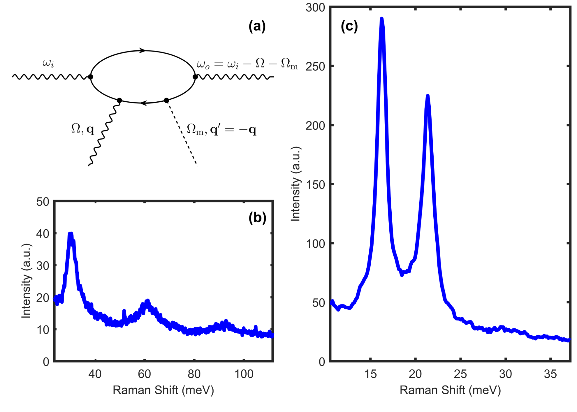
At first glance one should expect little from the Raman spectra of EuS. The crystal structure of EuS has two inter–penetrating face–centered cubic lattices and is symmetric under inversion. However, there is no unique center of inversion, and thus no modes that are even under inversion. A group theoretical analysis of the phonons in such a lattice reveals that at the zone center the optical modes are of symmetry and therefore Raman inactive. Despite this, in the EuX family of compounds (X = O, S, Se, Te) first–order Raman scattering is experimentally observedMerlin et al. (1977); Schlegel and Wachter (1973); Grünberg et al. (1977); Güntherodt et al. (1979) as seen in FIG. 1(b). The underlying mechanism behind this symmetry forbidden scattering has its origins in the spin–disorder present in the paramagnetic phaseMerlin et al. (1977). While phonons from throughout the Brillouin zone are not typically excited by optical means due to conservation of momentum, in these materials the disordered spin system is capable of providing the necessary momentum to balance out the phonon contributionGüntherodt et al. (1979). In particular, the LO phonon mode at the L point in the Brillouin zone has been shown to be excited in this scattering eventGrünberg et al. (1977); Güntherodt et al. (1979). The Feynman diagram for such a process is shown in FIG. 1(a). The incoming photon of energy excites an electron from the localized 4f valence band to the 5d conduction band, leaving behind a hole. The hole then interacts with both the lattice and the spin system, producing an LO phonon of energy and momentum , and a spin excitation with energy and momentum . The recombination of the electron and hole pair then emits the Raman scattered light of energy . Note that, although the spin system provides momentum , there is no energy cost associated with changing the spin since different spin states are degenerate in the paramagnetic phase (i.e., ). When the crystal has long–range magnetic order, the magnons at finite now require finite . However, the probability of creating a magnon via the Raman process is proportional to . Therefore as the system approaches and passes through its Curie temperature, the intensity of the Raman scattering is quenchedSchlegel and Wachter (1973); Güntherodt et al. (1979).
Since this is a higher order scattering process involving the excitation of both a phonon and a spin, the mode intensity might be expected to be weak. However, such a process is also highly resonant with the excitation energy. By tuning the laser to the right intermediate electronic state, the intensity of the EuS mode is strongly enhanced. Indeed, measurements of the scattering intensity as a function of excitation wavelength indicate that there is a strong resonance effect which has a maximum in the 2.2 eV rangeMerlin et al. (1977). Alternatively, we can achieve a similar enhancement (or suppression) by tuning the Fermi energy and changing the states involved in the optical transition. As a result of this, either through entering the magnetically ordered state, tuning the intermediate state by choice of laser or doping we can eliminate the Raman scattering from EuS.
The reported magnetic order at room temperature in EuS/Bi2Se3 heterostructures should thus also lead to a strong suppression of the magnetic Raman signatures at ambient temperatures. We explored this possibility with a series of EuS/Bi2Se3 samples with varying EuS thicknesses grown on two different substrates. This allowed us to also investigate the role of strain in these samples. Raman spectra were acquired using a WITec alpha300R confocal Raman system (detailed information about the synthesis of the heterostructures may be found inKatmis et al. (2016)). A 100X objective was used to focus the unpolarized, 532 nm (2.33 eV) light down to a 1 m spot size. A power of 10 W was used to avoid local heating of the Bi2Se3Zhao et al. (2011). Unphysical artifacts from “cosmic rays” were removed using an algorithm based on wavelet transformations and data clustering methodsTian and Burch (2016). Spectra that have had cosmic rays removed were averaged and normalized by power and integration time.
At room temperature, bare EuS should be in the paramagnetic phase and display a measurable Raman response. The results of our room temperature measurements on a film of 5 nm thick EuS (sapphire substrate) are shown in FIG. 1(b). As previously observed in the bulk, the spectrum clearly displays the fundamental mode at 30.4 meV as well as the second and third harmonic overtones (at 60.8 and 91.2 meV respectively). Our measured value for the fundamental is slightly higher than the typical room temperature value of 29.8 meVSchlegel and Wachter (1973); Merlin et al. (1977); Grünberg et al. (1977). While the reason for this shift is unclear, the ease of observation of the mode is consistent with the expectation of paramagnetism at ambient temperatures.
Surprisingly we find that the Bi2Se3/EuS heterostructures lack the EuS mode. In FIG. 1(c) we show the spectra acquired from a sample with 10 nm thick EuS and 7 QL thick Bi2Se3. While there are two peaks which belong to the Bi2Se3 (these are discussed later) the EuS mode is conspicuously absent. The thickness of the EuS layer is double that of the bare EuS sample, yet we still do not observe any corresponding Raman signatures. This is the case for every heterostructure that we measured, regardless of EuS or Bi2Se3 thickness. One possible explanation is the previously reported room temperature ferromagnetism has suppressed the magnetic excitation. Alternatively, there are two physical effects unrelated to the magnetism that may alter the Raman spectra.
The Raman from EuS could be suppressed by modifications of the electronic system. In the typical EuS Raman scattering process an electron is excited to the 5 conduction band and leaves a hole behind in the localized 4 valence band. The rest of the scattering process then proceeds as illustrated in FIG. 1(a). This process is highly resonant upon laser excitation energy with an amplification of two orders of magnitude occurring at our excitation energy of 2.33 eV, which is very nearly at the maximum of the resonanceMerlin et al. (1977). Such resonance is typically observed when the transitions in the scattering process involve real energy levels instead of virtual energy levelsCardona (1983). An implicit assumption in this discussion has been that the EuS is undoped and the Fermi level lies within the band gap of the EuS. However, if the EuS were to become doped and the Fermi level shifted into either the conduction or valence bands then we would have a change in the energy levels involved in the scattering process.
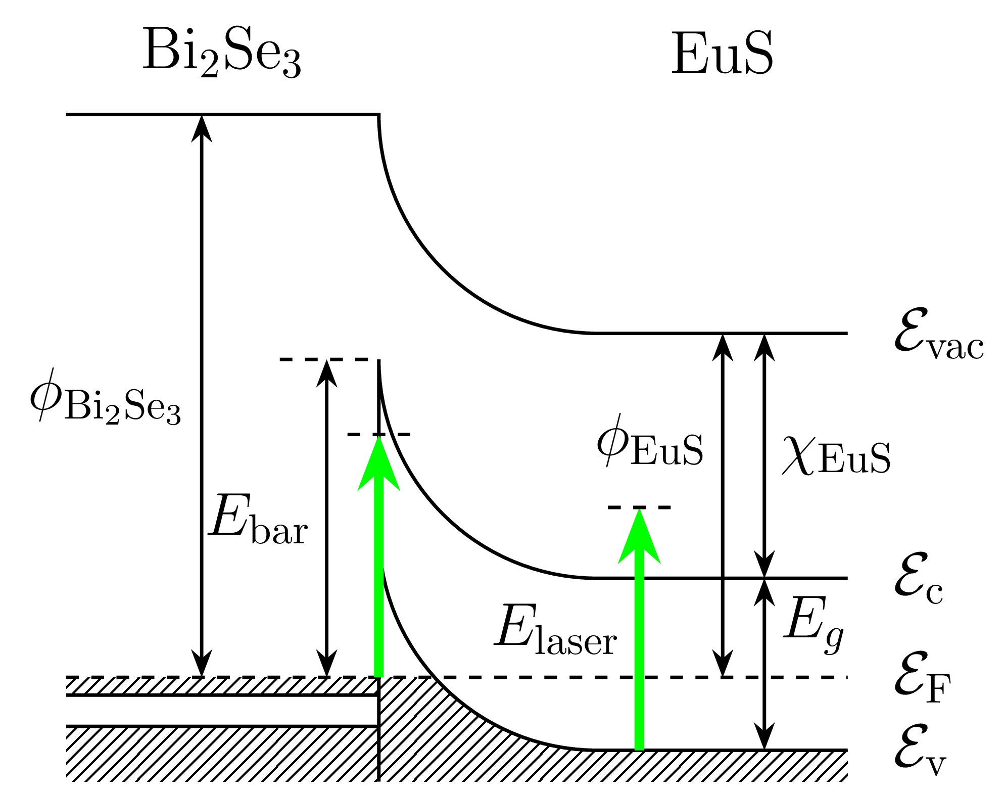
In fact, such a change in Fermi level is possible due to the band bending and the charge transfer that occurs at the Bi2Se3/EuS interface. In a simple model we may treat their interface as a metal–semiconductor junction, since the Bi2Se3 is sufficiently -doped ( cm-3) placing the Fermi energy deep in the conduction bandKatmis et al. (2016). The amount that the EuS bands will bend at the interface depends on the difference in work function between the two materials. Bi2Se3 has a work function of 5.4 eV and EuS has a work function of 3.3 eV (and electron affinity of 2.35 eV)Edmonds et al. (2014); Eastman et al. (1969).
In FIG. 2 we show a schematic of the band bending that occurs as a result of this mismatch. In order for the chemical potential at the interface between the two materials to be equal, electrons flow out of the EuS into the Bi2Se3. The barrier height formed at the interface is found as the difference between the work function of the Bi2Se3 and the EuS: eV. The difference between the barrier height and the 1.65 eV band gap in EuS tells us that the built-in potential is 1.4 eV. In other words, the Fermi level in the EuS is shifted down into the valence band by 1.4 eV. The spatial extent of this depleted layer is expected to be on the order of hundreds of nanometers and since our EuS films are only nanometers thick we expect that the entire layer experiences this effect. In the bare EuS our laser energy of 2.33 eV is capable of exciting electrons across the bandgap of 1.65 eV. However in the Bi2Se3/EuS heterostructure, the large shift in chemical potential requires eV to optically excite from the valence to conduction bands. The only available transitions for Raman scattering will then involve virtual energy levels, drastically reducing the intensity. This provides a natural explanation for the observed absence of the mode in our spectra. It is possible that future Raman experiments using a laser with higher energy per photon could be performed which would enable the observation of the EuS Raman mode.
Interestingly the band bending and associated introduction of holes into the EuS could be partially responsible for the previously reported increase in TC. Furthermore, should magnetic order be present at room temperature this could also explain the lack of a signal from the EuS. Unfortunately attempts to heat the sample above TC to observe the re-emergence of the peak were unsuccessful. Thus further studies are warranted, perhaps with ionic liquid gating or alternate capping layers to further elucidate the role of doping in our results.
A second explanation for the mode’s absence is Fabry–Perot interference due to the multi–layered nature of the samples. In a multi-layered structure there is the possibility of multiple reflections interfering with each other and either enhancing or suppressing both the incident laser and Raman scattered radiationNemanich et al. (1980); Ramsteiner et al. (1989). In order to address the role of interference, we performed numerical calculations that take into account multiple reflections at each interface. Similar calculations have been performed for a wide variety of quasi–two dimensional systems and were successful in explaining the variation in intensity with the thickness of the dielectric or exfoliated layersBlake et al. (2007); Wang et al. (2008); Yoon et al. (2009); Zhang et al. (2015); Sandilands et al. (2010); Zhao et al. (2011).
We developed an extension of the multi-reflection model (MRM) used by Zhang et al.Zhang et al. (2015). A diagram representing each of the two interference processes considered in the calculations is shown in FIG. 3. The first of these, illustrated in FIG. 3(a), is the interference of the incident laser with itself while the second, illustrated in FIG. 3(b), is the interference of the Raman scattered light. The model considers light at normal incidence, the rays are drawn at non–normal angles of incidence for clarity only. Details of the derivation for the enhancement factor may be found in the supplemental information.
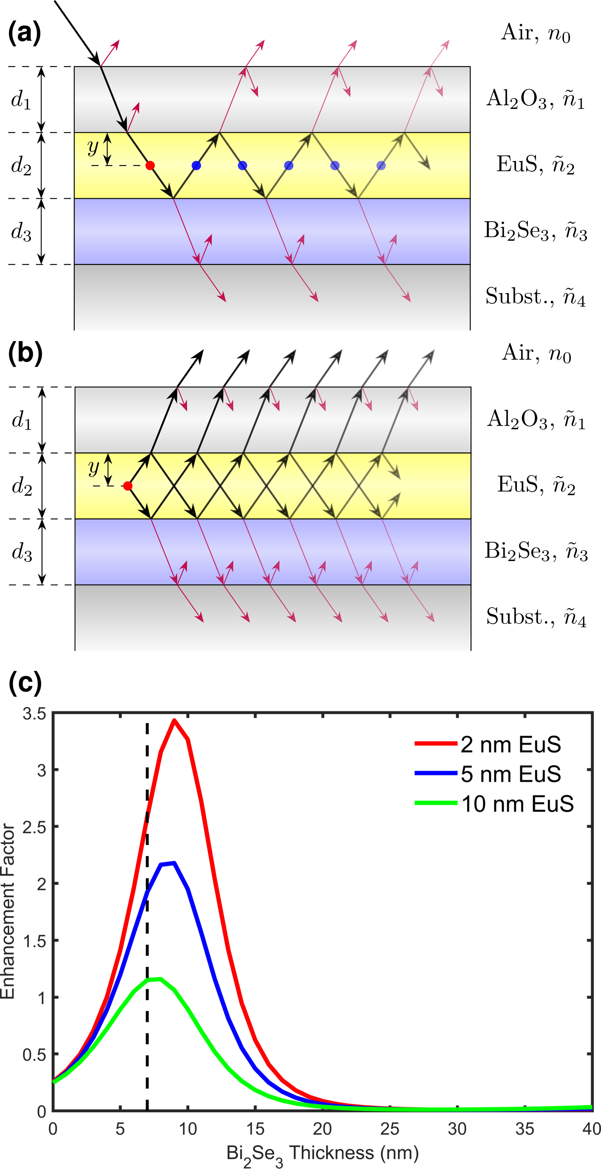
In FIG. 3(c) we show the interference enhancement factor obtained at the energy of the EuS Raman mode as a function of the Bi2Se3 thickness. The Al2O3 capping layer was fixed at 5 nm thick and the calculation repeated for multiple thicknesses of EuS. In the absence of a Bi2Se3 layer, i.e. when the thickness is zero, we see that we obtain an enhancement factor of 0.25. This indicates that, as expected due to the light exiting the back surface of the sample and the small volume, Raman signal from a thin slab of EuS will be reduced compared with a bulk crystal. In contrast, we see that at the thickness of Bi2Se3 in our samples, indicated by the dashed line, we obtain an enhancement factor of 2.5, 1.9, and 1.2 for EuS thicknesses of 2, 5, and 10 nm respectively. We should therefore expect to see a , , or times larger signal from the AlOx/EuS/Bi2Se3/sapphire films compared to just AlOx/EuS/sapphire. However, as seen in the measured spectra this is clearly not the case. We therefore rule out the possibility of FP interference causing the absence of the EuS Raman mode.
While the charge transfer discussed above seems to provide an explanation for the absence of the EuS Raman mode we can also investigate the role of the lattice in the enhancement through the spectral features associated with Bi2Se3. The interfacial strain between EuS and Bi2Se3 produces measurable effects on the phonons of the Bi2Se3 from which we can characterize the nature of the strain as well as the uniformity of the films. The results of our measurements may be found in the supplemental, but to summarize our analysis we find that there are different types of strain experienced by the Bi2Se3 depending on the type of substrate it is grown on. In the case of a sapphire substrate the Bi2Se3 experiences a tensile strain causing the phonon modes to shift down in energy, while with an STO substrate the strain is compressive, causing the phonon modes to shift up in energy. The addition of EuS adds another source of tensile strain that competes with the strain from the substrate, as observed through the dependence of the energy shifts on the thickness of the EuS layer. From Newton’s third law we infer that if EuS exerts a tensile strain on Bi2Se3 then the Bi2Se3 must exert a compressive strain on EuS. However, films with various Bi2Se3 thicknesses and substrates displayed similar TC enhancement, despite the large differences in the strain that we observed. This is somewhat surprising, given that a reduction in the lattice constant of EuS is known to increase the strength of the magnetic interactions and lead to higher Katmis et al. (2016); Goncharenko and Mirebeau (1998); Söllinger et al. (2010).
In summary, we have performed a series of Raman measurements on Bi2Se3/EuS heterostructures. The EuS Raman mode, which is an indicator of the degree of magnetic ordering, is not observed in heterostructures. While this could be a confirmation of the presence of ferromagnetism in the films at room temperature, there are other effects that could also be obscuring the observation of this mode. Our numerical calculations of optical interference indicate that this is not likely to be the cause, but rather charge transfer from the EuS is suppressing this mode. Such large charge transfer could open an additional pathway for tuning of the magnetic, optical, and electronic response of topological heterostructures. We also observed large changes in the Bi2Se3 phonons due to strain induced by EuS. This confirms a strong elastic coupling between the materials that could be exploited in future devices.
References
- Zhang et al. (2009) H. Zhang, C.-X. Liu, X.-L. Qi, X. Dai, Z. Fang, and S.-C. Zhang, Nature Physics 5, 438 (2009).
- Chen et al. (2009) Y. L. Chen, J. G. Analytis, J.-H. Chu, Z. K. Liu, S.-K. Mo, X. L. Qi, H. J. Zhang, D. H. Lu, X. Dai, Z. Fang, S. C. Zhang, I. R. Fisher, Z. Hussain, and Z.-X. Shen, Science 325, 178 (2009), http://science.sciencemag.org/content/325/5937/178.full.pdf .
- Hsieh et al. (2009) D. Hsieh, Y. Xia, D. Qian, L. Wray, F. Meier, J. H. Dil, J. Osterwalder, L. Patthey, A. V. Fedorov, H. Lin, A. Bansil, D. Grauer, Y. S. Hor, R. J. Cava, and M. Z. Hasan, Phys. Rev. Lett. 103, 146401 (2009).
- Lee et al. (2016a) C. Lee, F. Katmis, P. Jarillo-Herrero, J. Moodera, and N. Gedik, Nat. Commun. 7, 12014 (2016a).
- Yang et al. (2013) Q. I. Yang, M. Dolev, L. Zhang, J. Zhao, A. D. Fried, E. Schemm, M. Liu, A. Palevski, A. F. Marshall, S. H. Risbud, and A. Kapitulnik, Phys. Rev. B 88, 081407 (2013).
- Kandala et al. (2013) A. Kandala, A. Richardella, D. W. Rench, D. M. Zhang, T. C. Flanagan, and N. Samarth, Applied Physics Letters 103, 202409 (2013), http://dx.doi.org/10.1063/1.4831987.
- Li et al. (2015) M. Li, C.-Z. Chang, B. J. Kirby, M. E. Jamer, W. Cui, L. Wu, P. Wei, Y. Zhu, D. Heiman, J. Li, and J. S. Moodera, Phys. Rev. Lett. 115, 087201 (2015).
- Katmis et al. (2016) F. Katmis, V. Lauter, F. S. Nogueira, B. A. Assaf, M. E. Jamer, P. Wei, B. Satpati, J. W. Freeland, I. Eremin, D. Heiman, P. Jarillo-Herrero, and J. S. Moodera, Nature 533, 513 (2016).
- Chen et al. (2010) Y. L. Chen, J.-H. Chu, J. G. Analytis, Z. K. Liu, K. Igarashi, H.-H. Kuo, X. L. Qi, S. K. Mo, R. G. Moore, D. H. Lu, M. Hashimoto, T. Sasagawa, S. C. Zhang, I. R. Fisher, Z. Hussain, and Z. X. Shen, Science 329, 659 (2010), http://science.sciencemag.org/content/329/5992/659.full.pdf .
- Chang et al. (2013) C.-Z. Chang, J. Zhang, X. Feng, J. Shen, Z. Zhang, M. Guo, K. Li, Y. Ou, P. Wei, L.-L. Wang, Z.-Q. Ji, Y. Feng, S. Ji, X. Chen, J. Jia, X. Dai, Z. Fang, S.-C. Zhang, K. He, Y. Wang, L. Lu, X.-C. Ma, and Q.-K. Xue, Science 340, 167 (2013), http://science.sciencemag.org/content/340/6129/167.full.pdf .
- Kou et al. (2015) X. Kou, Y. Fan, M. Lang, P. Upadhyaya, and K. L. Wang, Solid State Communications 215–216, 34 (2015).
- Mellnik et al. (2014) A. Mellnik, J. Lee, A. Richardella, J. Grab, P. Mintun, M. Fische, A. Vaezi, A. Manchon, E.-A. Kim, N. Samarth, and D. Ralph, Nature 511, 449 (2014).
- Li et al. (2014) C. Li, M. van ’t Erve, J. Robinson, Y. Liu, L. Li, and B. Jonker, Nature Nanotechnology 9, 218 (2014).
- Cen et al. (2008) C. Cen, S. Thiel, C. Hammerl, G.and Schneider, K. Andersen, C. Hellberg, J. Mannhart, and J. Levy, Nature Materials 7, 298 (2008).
- Wang et al. (2016a) L. Wang, X. Ma, and Q.-K. Xue, Superconductor Science and Technology 29, 123001 (2016a).
- Hellman et al. (2016) F. Hellman, A. Hoffmann, Y. Tserkovnyak, G. Beach, E. Fullerton, C. Leighton, A. MacDonald, D. Ralph, D. Arena, H. Durr, P. Fischer, J. Grollier, J. Heremans, T. Jungwirth, A. Kimmel, B. Koopmans, I. Krivorotov, S. May, A. Petford-Long, J. Rondinelli, N. Samarth, I. Schuller, A. Slavin, M. Stiles, O. Tchernyshyov, A. Thiaville, and B. Zink, “Interface-induced phenomena in magnetism,” (2016), arXiv:1607.00439, arXiv:1607.00439 [cond-mat.mtrl-sci] .
- Reijnders et al. (2014) A. A. Reijnders, J. Hamilton, V. Britto, J.-B. Brubach, P. Roy, Q. D. Gibson, R. J. Cava, and K. S. Burch, Phys. Rev. B 90, 235144 (2014).
- Wang et al. (2012) Y. H. Wang, D. Hsieh, E. J. Sie, H. Steinberg, D. R. Gardner, Y. S. Lee, P. Jarillo-Herrero, and N. Gedik, Phys. Rev. Lett. 109, 127401 (2012).
- Kim et al. (2012) D. Kim, Q. Li, P. Syers, N. P. Butch, J. Paglione, S. D. Sarma, and M. S. Fuhrer, Phys. Rev. Lett. 109, 166801 (2012).
- Sandilands et al. (2010) L. J. Sandilands, J. X. Shen, G. M. Chugunov, S. Y. F. Zhao, S. Ono, Y. Ando, and K. S. Burch, Phys. Rev. B 82, 064503 (2010).
- Ferrari and Basko (2013) A. Ferrari and D. Basko, Nature Nanotechnology 8, 235 (2013).
- Wang et al. (2016b) X. Wang, K. Du, Y. Y. F. Liu, P. Hu, J. Zhang, Q. Zhang, M. H. S. Owen, X. Lu, C. K. Gan, P. Sengupta, C. Kloc, and Q. Xiong, 2D Materials 3, 031009 (2016b).
- Lee et al. (2016b) J.-U. Lee, S. Lee, J. H. Ryoo, S. Kang, T. Y. Kim, P. Kim, C.-H. Park, J.-G. Park, and H. Cheong, Nano Letters 16, 7433 (2016b), pMID: 27960508, http://dx.doi.org/10.1021/acs.nanolett.6b03052 .
- Tian et al. (2016) Y. Tian, M. J. Gray, H. Ji, R. J. Cava, and K. S. Burch, 2D Materials 3, 025035 (2016).
- Schlegel and Wachter (1973) A. Schlegel and P. Wachter, Solid State Communications 13, 1865 (1973).
- Merlin et al. (1977) R. Merlin, R. Zeyher, and G. Güntherodt, Phys. Rev. Lett. 39, 1215 (1977).
- Grünberg et al. (1977) P. Grünberg, G. Güntherodt, A. Frey, and W. Kress, Physica B+C 89, 225 (1977).
- Güntherodt et al. (1979) G. Güntherodt, R. Merlin, and P. Grünberg, Phys. Rev. B 20, 2834 (1979).
- Zhao et al. (2011) S. Y. F. Zhao, C. Beekman, L. J. Sandilands, J. E. J. Bashucky, D. Kwok, N. Lee, A. D. LaForge, S. W. Cheong, and K. S. Burch, Applied Physics Letters 98, 141911 (2011), http://dx.doi.org/10.1063/1.3573868.
- Tian and Burch (2016) Y. Tian and K. S. Burch, Applied Spectroscopy (2016), 10.1177/0003702816671065, http://asp.sagepub.com/content/early/2016/10/17/0003702816671065.full.pdf+html .
- Cardona (1983) M. Cardona, Light Scattering in Solids I, 2nd ed., Vol. 8 (Springer-Verlag Berlin Heidelberg, 1983).
- Edmonds et al. (2014) M. T. Edmonds, J. T. Hellerstedt, A. Tadich, A. Schenk, K. M. O’Donnell, J. Tosado, N. P. Butch, P. Syers, J. Paglione, and M. S. Fuhrer, ACS Nano 8, 6400 (2014), pMID: 24911767, http://dx.doi.org/10.1021/nn502031k .
- Eastman et al. (1969) D. E. Eastman, F. Holtzberg, and S. Methfessel, Phys. Rev. Lett. 23, 226 (1969).
- Nemanich et al. (1980) R. J. Nemanich, C. C. Tsai, and G. A. N. Connell, Phys. Rev. Lett. 44, 273 (1980).
- Ramsteiner et al. (1989) M. Ramsteiner, C. Wild, and J. Wagner, Appl. Opt. 28, 4017 (1989).
- Blake et al. (2007) P. Blake, E. W. Hill, A. H. Castro Neto, K. S. Novoselov, D. Jiang, R. Yang, T. J. Booth, and A. K. Geim, Applied Physics Letters 91, 063124 (2007), http://dx.doi.org/10.1063/1.2768624.
- Wang et al. (2008) Y. Y. Wang, Z. H. Ni, Z. X. Shen, H. M. Wang, and Y. H. Wu, Applied Physics Letters 92, 043121 (2008), http://dx.doi.org/10.1063/1.2838745.
- Yoon et al. (2009) D. Yoon, H. Moon, Y.-W. Son, J. S. Choi, B. H. Park, Y. H. Cha, Y. D. Kim, and H. Cheong, Phys. Rev. B 80, 125422 (2009).
- Zhang et al. (2015) H. Zhang, Y. Wan, Y. Ma, W. Wang, Y. Wang, and L. Dai, Applied Physics Letters 107, 101904 (2015), http://dx.doi.org/10.1063/1.4930257.
- Goncharenko and Mirebeau (1998) I. N. Goncharenko and I. Mirebeau, Phys. Rev. Lett. 80, 1082 (1998).
- Söllinger et al. (2010) W. Söllinger, W. Heiss, R. T. Lechner, K. Rumpf, P. Granitzer, H. Krenn, and G. Springholz, Phys. Rev. B 81, 155213 (2010).