Large tunable valley splitting in edge-free graphene quantum dots on boron nitride
Coherent manipulation of binary degrees of freedom is at the heart of modern quantum technologies. Graphene offers two binary degrees: the electron spin and the valley.
Efficient spin control has been demonstrated in many solid state systems, while exploitation of the valley has only recently been started, yet without control on the single electron level.
Here, we show that van-der Waals stacking of graphene onto hexagonal boron nitride offers a natural platform for valley control.
We use a graphene quantum dot induced by the tip of a scanning tunneling microscope and demonstrate valley splitting that is tunable from -5 to +10 meV (including valley inversion) by sub-10-nm displacements of the quantum dot position.
This boosts the range of controlled valley splitting by about one order of magnitude.
The tunable inversion of spin and valley states should enable coherent superposition of these degrees of freedom as a first step towards graphene-based qubits.
Electrical control is a central requirement to exploit the binary degrees of freedom of a single electron in a scalable way 1. This has been realized for spin systems using, e.g., small shifts of the electron spin within the field of a micro-magnet 2, 3. The valley degree of electrons has recently been detected in transport experiments on graphene 4, 5, 6, 7, 8, 9, but its control on the single electron level has not been achieved. Alternative materials, such as Si 10, offer only very small tuning ranges of the valley splitting by less than 0.5 meV 5, 11, 12, 13, 14, 15.
The valley degree of freedom in graphene is a consequence of the honeycomb structure with its two atoms within the unit cell 16, 17. Hence, breaking the equivalence of the two atoms (sublattice symmetry breaking) is the natural avenue to break the valley degeneracy as a starting point for tuning. This indeed works straightforwardly, if the time reversal symmetry is additionally broken, e.g., by a magnetic field 18. The sublattice symmetry breaking can be achieved by van-der Waals stacking of 2D materials exploiting the different stacking of the two graphene atoms on top of the supporting atoms. This stacking moreover spatially varies due to the different lattice constants of the adjacent materials 19, 20, 21, implying a spatially varying valley splitting which we exploit in our experiment.
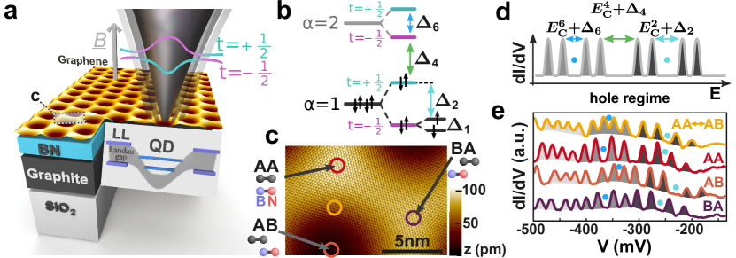
We have recently demonstrated smoothly confined Dirac fermions in an edge-free graphene quantum dot (QD) by combining the electric field of the tip with a perpendicular field (Fig. 1a) 22. The field quantizes the continuous spectrum of graphene in terms of Landau levels (LLs, LL spacing 100 meV at T) 18. The electric field of the tip exploits the energy gaps between LLs to achieve edge-free confinement, i.e., it shifts energy levels from the LLs into the gap 22. We thereby overcome the well-known problem of edge localization within etched graphene QDs 23. By confining without resorting to physical edges, these dots preserve the two-fold valley and spin symmetries of pristine graphene (Fig. 1b, d).
The charging of the confined levels has been directly measured by tuning the voltage of the STM tip such that the states cross the Fermi level . This revealed the most regularly spaced charging sequence of graphene QDs achieved to date 22. The measured level separations have been reproduced with the help of tight binding (TB) calculations. Hence, the charging peaks could be assigned to LLs and to particular orbital and valley states. Most notably, we observe quadruplets of charging peaks belonging to a single orbital quantum number of the dot and a partial splitting of single quadruplets into two doublets indicating the lifting of the valley degeneracy (Fig. 1b, d, e). This identification of the multiplet character goes far beyond the results achieved by chemical etching of monolayer graphene QDs 23 or double-sided gating of bilayer graphene QDs 24, 25, 26.
Movable quantum dot
Here, we explore the nanoscale variation of the charging sequence in detail. We use a heterostructure comprised of a SiO2/graphite support, a hexagonal boron nitride (hBN) substrate, and an active graphene layer on top which are assembled by the dry stacking method 27, 28 (Fig. 1a). The atomic lattices of graphene and hBN are collinearly aligned in order to create a hexagonal superlattice with lattice constant nm originating from the lattice mismatch of graphene and hBN.20 Different stacking regions of the C atoms with respect to the B and N atoms (Fig. 1c) naturally lead to a spatially varying adhesion energy as well as to a spatially varying sublattice symmetry breaking of graphene due to the inequivalent binding sites. The resulting structure has been extensively discussed in the literature 29, 30, 31, 32, 33, 34. It is known that the most attractive interaction is in the AB areas (Fig. 1c) leading to stretched central regions of graphene with AB stacking and closest contact to the hBN. These areas are surrounded by compressed graphene ridges of different stacking with larger separation to the hBN 30, 20. However, firm conclusions on the details of the superstructure are difficult to draw, because of the lack of knowledge of details of the van-der-Waals interaction 35.
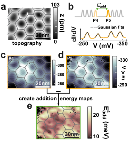
The tip induced graphene QD can be moved across the graphene superstructure by moving the STM tip 37. This allows to tune the QD properties, which we probe by tracking the position of the charging peaks within the superlattice. Therefore, we employ spatially resolved spectra (: tunneling current, : tip voltage). The resulting maps of charging energies can be directly compared with the corresponding topographic maps recorded simultaneously (Fig. 2a). The charging peaks are fitted by Gaussians (Fig. 2b) for each QD center position , rendering maps of the local variation of the voltage of the peak, (Fig. 2c, d). Typical variations between the center and the boundary of the hexagonal supercell are mV. In order to relate this to an energy variation of a particular QD level, we employ a capacitive model yielding with the lever arm 38 and electron charge . The variations are primarily caused by the spatially varying adhesion energy across the supercell, which indeed varies on the 10 meV-scale according to extensive model calculations 30. Figure 2c and d additionally exhibit a long-range variation on the 50 nm scale (amplitude mV) which we attribute to the uncontrolled, long-range disorder potential of graphene on hBN with strength of about 20 meV and correlation length of about 50 nm. Similar disorder potentials have been found previously 39, 40. Note that we carefully avoid lifting of the graphene layer by the tip forces, i.e., we regularly record curves (: tip-sample distance) verifying that the current remains below the threshold where a slope change of indicates lifting 41, 42.
Tracking orbital, valley and spin splitting
The group of the first four charging peaks, P1 to P4, is associated with the quadruplet belonging to the first hole orbital of the QD. During the charging of these levels, the QD exhibits a depth of about 100 and a width of about 50 as known from detailed Poisson calculations 38, 22. The confined wave functions are labeled with orbital quantum number for the first four peaks, valley quantum number and spin quantum number . Analogously, the next four peaks, P5 to P8, belong to the filling of the quadruplet . Subtracting the voltage of the highest peak of the first quadruplet (Fig. 2c) from that of the lowest peak of the second, (Fig. 2d), and multiplying by , yields the locally varying addition energy map (Fig. 2e). It consists of the charging energy and the energy difference . The latter includes the valley splitting and the considerably smaller Zeeman splitting (: gyromagnetic factor of graphene, : Bohr magneton). The dominant contribution comes from the orbital splitting as known from tight binding calculations 22. Since the wave function size does not change strongly as a function of (see movie in supporting information), the spatial variation of cannot explain the strong spatial variation of , which varies by a factor of two. Hence, (Fig. 2e) mostly maps out the orbital-energy spacing between and , as the quantum dot is moved across the graphene superstructure. Periodic depressions in the center of the supercell reveal the influence of the superstructure on the orbital splitting, while the long-range structure in Fig. 2e (50 nm scale) is again attributed to the long-range potential disorder.
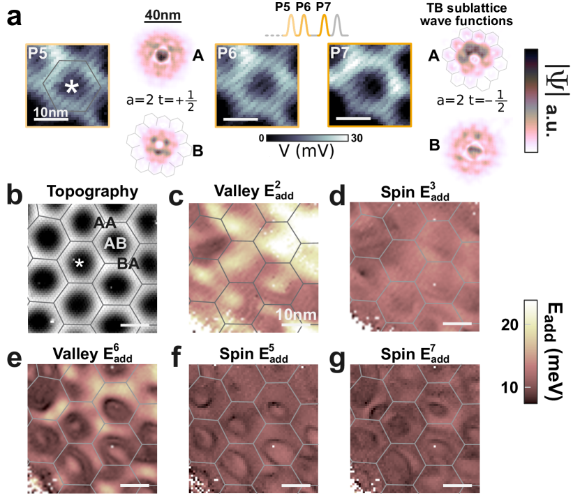
For clarity, we focus now on the second hole orbital shell (Fig. 3), while we provide other maps in the supplementary sections 4 and 5. The local variation of the voltage peaks belonging to the quadruplet allows to map out valley and spin splittings in detail. The voltage maps, and , differ on length scales well below that of the supercell size ( nm), and much smaller than the size of the QD wave function (diameter nm, calculated by our TB approach) (Fig. 3a). The addition energy maps (Fig. 3eg) clearly display short-range supercell-periodic variations on the length scale of nm. These variations appear as dark, ring-like structures around the AB stacking region of the supercell in the valley addition energy map . Similar, but slightly narrower rings appear in the spin addition energy maps and .
Analyzing the valley splitting maps
We analyze these remarkably strong nanometer scale variations by performing TB calculations 43, 31. The calculations feature three major ingredients: (i) the sublattice-independent local on-site potential representing the spatially varying adhesion energy, (ii) the sublattice symmetry-breaking on-site potential caused by the spatially varying stacking, and (iii) a locally varying hopping amplitude accounting for strain which also breaks sublattice symmetry 18, 42, 34. We use an average distance between graphene and hBN of Å, originating from DFT calculations employing the random phase approximation 29 and consistent with cross sectional electron microscopy data 44. To obtain locally varying tight-binding parameters, we first employ a continuum model of graphene with known elastic constants 32 subject to the potential landscape from the hBN 30. This reproduces the corrugation of 70 pm and the strain variation of 2 %, as visible in the STM data (Fig. 2a) 20. Based on the resulting membrane shape of the graphene layer, a molecular dynamics simulation using isotropic Lenard-Jones potentials is employed to obtain the atomically resolved strain, the variations in the local distance between hBN and graphene, and the local stacking configuration 38. Using these input parameters, we determine , and from our own DFT calculations 38. The potentials and hopping parameters provide, in turn, the input to our third-nearest neighbor TB calculation of the QD states 43, 31, 22. We emphasize that no freely adjustable parameter enters our simulation. More details are described in supplementary sections 7-10.
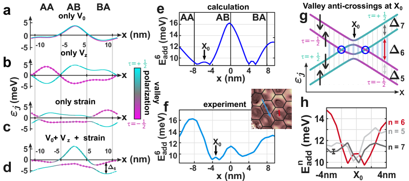
In agreement with the experiment, the calculated energies of the two valley states of the second orbital feature a pronounced variation with QD position (Fig. 4ad). To disentangle the influence of strain and of the hBN substrate interaction, we analyze the contributions due to , , and separately. While (Fig. 4a) introduces local variations of the energy of the hole orbital along the path AAABBA, it does not lift the fourfold valley and spin degeneracy. , by contrast, lifts the degeneracy between the two valley states and and even leads to an inversion of the energetic order in the AA region of the superlattice, i.e., a change of sign of (Fig. 4b). However, only when the contribution of strain is accounted for through , which inverts the sign of the valley splitting in the BA region (Fig. 4c), the correct overall level ordering with level inversion in the AB region, as seen in our experiment, emerges (Fig. 4d).
The addition energies in both, the TB model (Fig. 4e) and the experiment (Fig. 4f), show the same variation of about meV and the same order of maxima and minima along the displacement coordinate . Hence, we attribute the periodically appearing rings encircling the AB region (Fig. 3e), which correspond to the bump at with adjacent minima in Fig. 4e, as the positions of an inversion of valley ordering. Remaining quantitative differences between TB model and experiment (Fig. 4e, f) are attributed to disorder, most likely due to residual irregular strains caused by the non-perfect collinear alignment between graphene and hBN. The resulting disorder is directly visible as irregularities in the unit cell of the superstructure (Fig. 2a, Fig. 3b) and also explains the irregular distortions of the rings around the AB region.
The assignment of the rings around the AB region to valley inversions is corroborated by the appearance of the small bump in the ring minimum, marked in Fig. 4eh. It is found in theory and experiment with a height of less than 1 meV. The theoretical level diagram (Fig. 4g) provides a simple explanation: the bump is the result of the additional spin splitting during the passage through the crossing of valley levels. At , consists of and the spin splitting eV reduced by anti-crossing contributions. In contrast, the two spatially offset crossings of valley states with different spins (blue circles in Fig. 4g) feature only , resulting in the minima around the bump. Figure 4g also explains the rings in the spin splitting maps (Fig. 3f, g), which are simply the reduced and at . The spatial alignment of the bump in and the minima in are nicely corroborated by the experiment (Fig. 4h).
While we have focused here on the valley splitting of the second hole state, similar ring-like structures encircling the AB area are also found for the third hole orbital with tunability of the valley crossing up to 15 meV (Fig. S2) 38. In contrast, the first hole orbital (Fig. 3c, e) exhibits a valley tunability of about 7 meV without inversion of the valley ordering. On the electron side, the additional charging of defects within the h-BN 45 complicates the analysis 46, but some ring-like structures indicating valley inversion can also be spotted 38. Data recorded with another microtip at two different fields exhibit very similar features (Fig. S3). Moreover, the energy range of valley tunability remains independent of , corroborating that the valley tuning is caused by the interaction with the substrate and not by the field. For example, the strength of the exchange enhancement would vary with 38. In addition, it turns out to be one order of magnitude too weak to explain the experimentally observed valley tuning (supplementary section 12).
A simple estimate clarifies the resulting strength of the valley splitting of about 10 meV. The sublattice breaking interactions itself (, ) spatially vary by about 100 meV as deduced from our DFT calculations 38. Hence, shifting about 10% of the hole density of a state () from the unfavorable AB to the favorable AA region is sufficient to account for variations of the valley splitting of about 10 meV. Indeed, our detailed TB calculations find that the wave function covers about ten unit cells (Fig. 3a) and adjusts mainly its distribution within the central unit cell due to the changing potential landscape (supplemental movie).
Conclusions and outlook
The revealed tunability of a valley splitting by up to meV surpasses the highest reported values of valley tuning for other potentially nuclear spin free host materials (Si/SiO2, ) 5 by more than one order of magnitude. Hence, it might be exploited at temperatures up to 4 K. Most intriguingly, the crossings of valley and spin levels as depicted in Fig. 4g can be used to initialize superposition states of spin and valley degrees of freedom 2, 47. This could be the starting point to determine the coherence 48 of both types of states in graphene for the first time. The required interaction of the levels rendering the depicted crossings into anti-crossings is naturally provided by the spatially varying sublattice potential coupling opposite valley states (Fig. 4d). We note in passing that the breaking of the valley degeneracy is also the central requirement for exchange-based spin qubits, which could provide an all electrical spin qubit operation in graphene 49. A possible device setup for these purposes could employ side gates for moving gate-based QDs and, hence, for providing the valley tuning. Edge states, belonging to each LL, can provide tunable source and drain contacts (supplementary section 13).
Finally, we emphasize that the approach of designed van-der-Waals heterostructures 19, 20, 21 for a versatile tuning of electronic degrees of freedom might be extended to physical spin schemes by using an atomically varying spin orbit interaction as present, e.g., for graphene on WSe2 50.
Acknowledgements
The authors appreciate helpful discussions with C. Stampfer, H. Bluhm, R. Bindel, M. Liebmann, and K. Flöhr as well as the assisting during the measurements by A. Georgi. NMF, PNI and MM acknowledge support from the European Union Seventh Framework Programme under Grant Agreement No. 696656 (Graphene Flagship) and the German Science foundation (Li 1050-2/2 through SPP-1459), LAC, JB and FL from the Austrian Fonds zur Förderung der wissenschaftlichen Forschung (FWF) through the SFB 041-ViCom and doctoral college Solids4Fun (W1243). TB calculations were performed on the Vienna Scientific Cluster. RVG, AKG and KSN also acknowledge support from EPSRC (Towards Engineering Grand Challenges and Fellowship programs), the Royal Society, US Army Research Office, US Navy Research Office, US Airforce Research Office. KSN is also grateful to ERC for support via Synergy grant Hetero2D. AKG was supported by Lloyd’s Register Foundation. PNI acknowledges the support from the Hungarian Academy of Sciences Lendület grant no. LP2017-9/2017.
Author contributions
N.M.F. carried out the STM measurements with assistance of P.N.I. and C.H. and evaluated the experimental data under supervision of P.N.I. and M.M.; P.N.I. has performed the strain calculations, while T.R., F.L., and L.A.C. have contributed DFT and TB calculations; C.R.W., Y.C., R.V.G., A.K.G. and K.S.N. provided the sample; M.M. conceived and coordinated the project partly together with N.M.F., P.N.I. and F.L.; the comparison between theory and experiment has been conducted by N.M.F., M.M., F.L., and P.N.I.; M.M., N.M.F., P.N.I. and F.L. wrote the manuscript with contributions from all authors.
References
- 1 Ladd, T. D. et al. Quantum computers. Nature 464, 45–53 (2010).
- 2 Pioro-Ladriere, M. et al. Electrically driven single-electron spin resonance in a slanting zeeman field. Nat. Phys. 4, 776–779 (2008).
- 3 Wu, X. et al. Two-axis control of a singlet-triplet qubit with an integrated micromagnet. Proc. Natl. Acad. Sci. U.S.A. 111, 11938–11942 (2014).
- 4 Abanin, D. A. et al. Giant Nonlocality Near the Dirac Point in Graphene. Science 332, 328–330 (2011).
- 5 Yang, C. H. et al. Spin-valley lifetimes in a silicon quantum dot with tunable valley splitting. Nat. Commun. 4, 2069 (2013).
- 6 Shimazaki, Y. et al. Generation and detection of pure valley current by electrically induced Berry curvature in bilayer graphene. Nat. Phys. 11, 1032–1036 (2015).
- 7 Sui, M. et al. Gate-tunable topological valley transport in bilayer graphene. Nat. Phys. 11, 1027–1031 (2015).
- 8 Ju, L. et al. Topological valley transport at bilayer graphene domain walls. Nature 520, 650–655 (2015).
- 9 Wallbank, J. R. et al. Tuning the valley and chiral quantum state of Dirac electrons in van der Waals heterostructures. Science 353, 575–579 (2016).
- 10 Rahman, R. et al. Engineered valley-orbit splittings in quantum-confined nanostructures in silicon. Phys. Rev. B 83, 195323 (2011).
- 11 Gokmen, T. et al. Parallel magnetic-field tuning of valley splitting in alas two-dimensional electrons. Phys. Rev. B 78, 233306 (2008).
- 12 Kobayashi, T. et al. Resonant tunneling spectroscopy of valley eigenstates on a donor-quantum dot coupled system. Appl. Phys. Lett. 108, 152102 (2016).
- 13 Gamble, J. K. et al. Valley splitting of single-electron si MOS quantum dots. Appl. Phys. Lett. 109, 253101 (2016).
- 14 Scarlino, P. et al. Dressed photon-orbital states in a quantum dot: Intervalley spin resonance. Phys. Rev. B 95, 165429 (2017).
- 15 Mi, X., Péterfalvi, C. G., Burkard, G. & Petta, J. High-resolution valley spectroscopy of Si quantum dots. Phys. Rev. Lett. 119, 176803 (2017).
- 16 Xiao, D., Yao, W. & Niu, Q. Valley-contrasting physics in graphene: Magnetic moment and topological transport. Phys. Rev. Lett. 99, 236809 (2007).
- 17 Pesin, D. & MacDonald, A. H. Spintronics and pseudospintronics in graphene and topological insulators. Nat. Mater. 11, 409–416 (2012).
- 18 Castro Neto, A. H., Guinea, F., Peres, N. M. R., Novoselov, K. S. & Geim, A. K. The electronic properties of graphene. Rev. Mod. Phys. 81, 109–162 (2009).
- 19 Geim, A. K. & Grigorieva, I. V. Van der waals heterostructures. Nature 499, 419–425 (2013).
- 20 Woods, C. R. et al. Commensurate-incommensurate transition in graphene on hexagonal boron nitride. Nat. Phys. 10, 451–456 (2014).
- 21 Novoselov, K. S., Mishchenko, A., Carvalho, A. & Castro Neto, A. H. 2D materials and van der Waals heterostructures. Science 353, 461–470 (2016).
- 22 Freitag, N. M. et al. Electrostatically confined monolayer graphene quantum dots with orbital and valley splittings. Nano Lett. 16, 5798–5805 (2016).
- 23 Bischoff, D. et al. Localized charge carriers in graphene nanodevices. Appl. Phys. Rev. 2, 031301 (2015).
- 24 Allen, M. T., Martin, J. & Yacoby, A. Gate-defined quantum confinement in suspended bilayer graphene. Nat. Commun. 3, 934 (2012).
- 25 Goossens, A. M. et al. Gate-defined confinement in bilayer graphene-hexagonal boron nitride hybrid devices. Nano Lett. 12, 4656–4660 (2012).
- 26 Müller, A. et al. Bilayer graphene quantum dot defined by topgates. J. Appl. Phys. 115, 233710 (2014).
- 27 Mayorov, A. S. et al. Micrometer-scale ballistic transport in encapsulated graphene at room temperature. Nano Lett. 11, 2396–2399 (2011).
- 28 Kretinin, A. V. et al. Electronic properties of graphene encapsulated with different two-dimensional atomic crystals. Nano Lett. 14, 3270–3276 (2014).
- 29 Sachs, B., Wehling, T. O., Katsnelson, M. I. & Lichtenstein, A. I. Adhesion and electronic structure of graphene on hexagonal boron nitride substrates. Phys. Rev. B 84, 195414 (2011).
- 30 van Wijk, M. M., Schuring, A., Katsnelson, M. I. & Fasolino, A. Moiré patterns as a probe of interplanar interactions for graphene on h-bn. Phys. Rev. Lett. 113, 135504 (2014).
- 31 Chizhova, L. A., Libisch, F. & Burgdörfer, J. Graphene quantum dot on boron nitride: Dirac cone replica and hofstadter butterfly. Phys. Rev. B 90, 165404 (2014).
- 32 San-Jose, P., Gutiérrez-Rubio, A., Sturla, M. & Guinea, F. Spontaneous strains and gap in graphene on boron nitride. Phys. Rev. B 90, 075428 (2014).
- 33 Slotman, G. J. et al. Effect of structural relaxation on the electronic structure of graphene on hexagonal boron nitride. Phys. Rev. Lett. 115, 186801 (2015).
- 34 Jung, J. et al. Moiré band model and band gaps of graphene on hexagonal boron nitride. Phys. Rev. B 96, 085442 (2017).
- 35 Ambrosetti, A., Ferri, N., DiStasio, R. A., Jr. & Tkatchenko, A. Wavelike charge density fluctuations and van der Waals interactions at the nanoscale. Science 351, 1171–1176 (2016).
- 36 Morgenstern, M. et al. Origin of landau oscillations observed in scanning tunneling spectroscopy on n-inas(110). Phys. Rev. B 62, 7257–7263 (2000).
- 37 Dombrowski, R., Steinebach, C., Wittneven, C., Morgenstern, M. & Wiesendanger, R. Tip-induced band bending by scanning tunneling spectroscopy of the states of the tip-induced quantum dot on inas(110). Phys. Rev. B 59, 8043–8048 (1999).
- 38 Freitag, N. et al. see supplementary information .
- 39 Xue, J. M. et al. Scanning tunnelling microscopy and spectroscopy of ultra-flat graphene on hexagonal boron nitride. Nat. Mater. 10, 282–285 (2011).
- 40 Decker, R. et al. Local electronic properties of graphene on a bn substrate via scanning tunneling microscopy. Nano Lett. 11, 2291–2295 (2011).
- 41 Mashoff, T. et al. Bistability and Oscillatory Motion of Natural Nanomembranes Appearing within Monolayer Graphene on Silicon Dioxide. Nano Lett. 10, 461–465 (2010).
- 42 Georgi, A. et al. Tuning the Pseudospin Polarization of Graphene by a Pseudomagnetic Field. Nano Lett. 17, 2240–2245 (2017).
- 43 Libisch, F., Rotter, S., Güttinger, J., Stampfer, C. & Burgdörfer, J. Transition to landau levels in graphene quantum dots. Phys. Rev. B 81, 245411 (2010).
- 44 Haigh, S. J. et al. Cross-sectional imaging of individual layers and buried interfaces of graphene-based heterostructures and superlattices. Nat. Mater. 11, 764–767 (2012).
- 45 Wong, D. et al. Characterization and manipulation of individual defects in insulating hexagonal boron nitride using scanning tunnelling microscopy. Nat. Nanotechnol. 10, 949–953 (2015).
- 46 Morgenstern, M., Freitag, N., Nent, A., Nemes-Incze, P. & Liebmann, M. Graphene quantum dots probed by scanning tunneling microscopy. Ann. d. Phys. 529, 1700018 (2017).
- 47 Petta, J. et al. Coherent manipulation of coupled electron spins in semiconductor quantum dots. Science 309, 2180–2184 (2005).
- 48 Elzerman, J. M. et al. Single-shot read-out of an individual electron spin in a quantum dot. Nature 430, 431 (2004).
- 49 Trauzettel, B., Bulaev, D. V., Loss, D. & Burkard, G. Spin qubits in graphene quantum dots. Nat. Phys. 3, 192–196 (2007).
- 50 Wang, Z. et al. Origin and Magnitude of ‘Designer’ Spin-Orbit Interaction in Graphene on Semiconducting Transition Metal Dichalcogenides. Phys. Rev. X 6, 041020 (2016).
Methods
The sample was prepared by exfoliating graphite flakes on a SiO2 substrate, followed by two consecutive dry transfers27, 28 of thick hexagonal hBN and monolayer graphene, respectively. During the graphene transfer, we took care to minimize the angular misalignment between the graphene lattice and the hBN lattice. Remaining small misalignments in the regime cannot be excluded 20. Moreover, a few small bubbles between the graphene and the h-BN apppear after transfer (see chapter S7 of Ref. 42). Both of these effects lead to mechanical stresses which perturb the graphene/BN superlattice in period or shape 1 (Fig. 2a and 3b of the main text). The graphene flake overlaps the hBN completely. This avoids insulating areas, which would be hazardous to the STM tip, but does not allow for back-gate operation. Finally, electrical Cr/Au contacts (/) are evaporated onto the large bottom graphite flake via a shadow mask. Optical images of the device structure are available in the supplement of a previous publication 22.
STM and STS measurements are performed in a home-built ultra-high-vacuum STM chamber operating at temperature K and in magnetic fields up to T perpendicular to the surface.2 Tungsten tips are prepared by etching of W wires, which are subsequently controlled with an optical microscope. The microtips are transferred into the STM within the UHV chamber, where they are reshaped by controlled indentation into the Au(111) surface of a Au bead.3
Thereby, they form a Au apex of a few in length as crosschecked by electron microscopy.
We characterize the tips in-situ by mapping the topographic and spectroscopic features of the Au(111) surface prior to exchanging the Au crystal by the graphene sample.
Scanning tunneling microscopy (STM) images are recorded in constant current mode at tunneling current and tip voltage .
Differential conductance curves are recorded by lock-in detection using a modulation voltage with amplitude and frequency . After stabilizing the tip-sample distance at stabilization voltage and stabilization current ,
the feedback loop is opened for the recording. During the recording, the tip-sample distance is changed at a rate of pm/V, approaching the sample by Å while sweeping from to and retracting it by the same distance while continuing to . This compensates for the changing height of the tunneling barrier as a function of .4
The resulting change in tip-sample capacitance is below %.22 It is, thus, neglected, since much smaller than other capacitance uncertainties (see below).
Additionally, we normalize the data according to with being the firstly detected current after opening the feedback loop. This compensates for the influence of vibrations during the stabilization process.
We focus on the first two orbital states for confined holes, originating from LL-1 (see below), as they capture the essential features.
On the electron side, charging of randomly distributed defects in the hBN 45 impedes an unambiguous analysis of the QD charging patterns (see Fig. S2 of the supplement) 22.
Data availability
The data that support the plots within this paper and other findings of this study are available from the corresponding author upon reasonable request.
Additional information
Supplementary information is available in the online version of the paper. Reprints and permission information is available online at www.nature.com/reprints. Correspondence and requests for materials should be addressed to M.M.
References
- 1 Jiang, Y. et al. Visualizing strain-induced pseudomagnetic fields in graphene through an hBN magnifying glass. Nano Lett. 17, 2839–2843 (2017).
- 2 Mashoff, T., Pratzer, M. & Morgenstern, M. A low-temperature high resolution scanning tunneling microscope with a three-dimensional magnetic vector field operating in ultrahigh vacuum. Rev. Sci. Instr. 80, 053702 (2009).
- 3 Voigtländer, B., Cherepanov, V., Elsaesser, C. & Linke, U. Metal bead crystals for easy heating by direct current. Rev. Sci. Instr. 79, 033911 (2008).
- 4 Feenstra, R. Tunneling spectroscopy of the (110)-surface of direct-gap III-V semiconductors. Phys. Rev. B 50, 4561–4570 (1994).