Mapping the band structure of GeSbTe phase change alloys around the Fermi level
Abstract
Phase change alloys are used for non-volatile random access memories exploiting the conductivity contrast between amorphous and metastable, crystalline phase. However, this contrast has never been directly related to the electronic band structure. Here, we employ photoelectron spectroscopy to map the relevant bands for metastable, epitaxial GeSbTe films. The constant energy surfaces of the valence band close to the Fermi level are hexagonal tubes with little dispersion perpendicular to the (111) surface. The electron density responsible for transport belongs to the tails of this bulk valence band, which is broadened by disorder, i.e., the Fermi level is 100 meV above the valence band maximum. This result is consistent with transport data of such films in terms of charge carrier density and scattering time. In addition, we find a state in the bulk band gap with linear dispersion, which might be of topological origin.
Introduction
Phase change alloys are the essential components for optical data storage (DVD-RW, Blu-ray Disc) and for electrically addressable phase-change random-access memories (PC-RAM)1; 2. The latter are envisioned to become more energy efficient using interfacial phase-change memories, whose phase change has been related to a topological phase transition3. Phase change alloys are typically chalcogenides consisting of Ge, Sb and Te (GST) with Ge2Sb2Te5 (GST-225) being the prototype1; 4. They exhibit three different structural phases: an amorphous, a metastable rock salt, and a stable trigonal phase. Switching the system from amorphous to metastable leads to a large contrast in electrical conductivity and optical reflectivity, which is exploited for data storage5; 6. Such switching favorably occurs within nanoseconds7; 8 and at an energy cost down to 1 fJ for a single cell9.
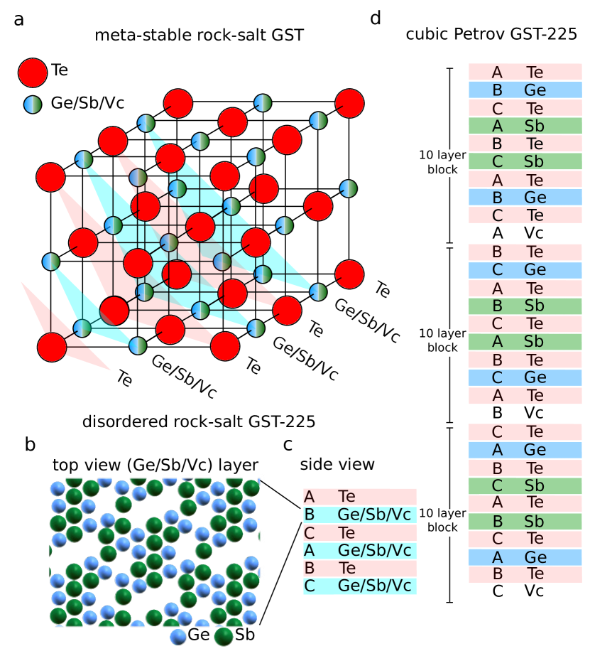
The technologically relevant, metastable phase10, usually obtained by rapid quenching from the melt, has a rock salt like structure with Te atoms at one sublattice and a mixture of randomly distributed Ge, Sb and vacancies (Vcs) on the other sublattice (Fig. 1a, b)11; 12; 13; 14. The stable phase consists of hexagonally close-packed layers of either Ge, Sb or Vcs with hexagonal layers of Te in between. Hence, the Vc layers bridge adjacent Te layers 15; 16. The stable phase has trigonal symmetry and is distinct in stacking of the hexagonal layers from the regular ABC stacking within the rock salt like metastable phase (Fig. 1c, d).
In the metastable phase, the disorder on the (Ge,Sb,Vc) site leads to Anderson localization of the electrons 17. The localization is lifted by annealing due to the respective continuous ordering of the Ge, Sb, and Vcs into different layers 18; 19; 20. This is accompanied by a shift of the Fermi level towards the valence band (VB)17; 21. However, the corresponding Fermi surface is not known as well as the exact position of , such that it is difficult to understand the electrical conductivity in detail.
Most of the electrical transport measurements so far were conducted using polycrystalline GST 17; 22, such that many established tools requiring crystallinity of the samples could not be applied. Only recently, epitaxial films of single crystalline quality have been achieved by molecular beam epitaxy (MBE)23; 24; 25; 20; 26. These films have been probed so far by X-ray diffraction (XRD), electron microscopy23; 24; 25; 20; 27; 26, magnetotransport studies20, Raman spectroscopy, and Fourier transform infrared spectroscopy26; 28. Most importantly, it was found that the epitaxial GST films are in the technologically relevant rock salt phase, but often exhibit ordering of the vacancies in separate layers20.
Here, we provide the first detailed measurement of the band structure of such epitaxial films by angular resolved photoelectron spectroscopy (ARPES). We focus on the nominal composition GST-225, and employ an ultrahigh-vacuum (UHV) transfer from the MBE system to prevent surface oxidation29 (see methods). Within the whole Brillouin zone (BZ), we find an M-shaped bulk VB in all directions parallel to the surface. This is in qualitative agreement with density functional theory (DFT) calculations of the cubic adaption of the trigonal Petrov phase15; 30, sketched in Fig. 1d. For brevity, we call this structure the cubic Petrov phase. Connecting the VB maxima of the experimental data results in a hexagonal tube at an energy about 100 meV below . Hence, the classical Fermi volume of a strictly periodic system would be zero, which contradicts the observation of metallic conductivity20. This apparent contradiction is solved by the significant broadening of the states due to disorder, such that there is still considerable weight of the valence band states above . The sum of these weights results in a charge carrier density consistent with the charge carrier density obtained from Hall measurements of the MBE films. The width of the states is, moreover, compatible with the scattering time deduced from the transport data. Such a detailed description of electrical transport provides a significant improvement over more simplistic models based on a parabolic and isotropic valence band as used so far17; 22.
Additionally, we find an electronic band within the fundamental bulk band gap of the metastable phase by two-photon ARPES. This band exhibits a largely isotropic, linear dispersion and circular dichroism such as known for topological surface states (TSS) 31; 32; 31; 33. We also find states close to the VB maximum with a strong in-plane spin polarization perpendicular to by conventional ARPES again similar to TSSs. A non-trivial topology of GST-225 has indeed been predicted for certain stacking configurations by DFT calculations34; 35; 36; 37; 38 and has been conjectured from the M-type VB dispersion39. Assuming that the Dirac-type state is indeed a TSS and, hence, cuts , it would contribute to the electronic transport. It would even dominate the conductivity, if its mobility is larger than . This is lower than the best TSS mobilities found in other topological insulators such as Bi2Se3 and BiSbTeSe2 films ()40; 41.
Results
Constant energy surfaces
ARPES experiments were performed at 29 different photon energies eV with a step size of eV. This allows a detailed determination of the dispersion of the bands (: wave vector perpendicular to the surface). Using the estimated crystal potential eV (methods), the chosen relate to Å-1. The ARPES spectra show an inverted M-shaped VB in energy-momentum cuts (EMCs) taken along the surface plane (Fig. 2d). The independently measured Fermi level is well above the VB maximum. Both is in line with earlier, less extensive results39. We label additionally with the superscript PES, since it differs from in DFT calculations with respect to the VB maximum. Figure 2a displays constant energy cuts (CECs) of the normalized photoelectron intensity (methods) at for selected . To determine peak positions, momentum distribution curves (MDCs) are extracted and fitted by Voigt peaks (Fig. 2b,c). The resulting peak momenta form a hexagonal tube (Fig. 2e,f) called the pseudo Fermi surface of GST-225. We call it pseudo, since the peak energies resulting from fits of energy distribution curves (EDCs) do not cross for any , as visible, e.g., in Fig. 2d. Consequently, there are no band centers at as required for a conventional Fermi surface 42. Only the tails of the broadened energy peaks cross . The sizes of the hexagons of the pseudo Fermi surface slightly vary with , i.e. along , with minimal diameter at eV (arrow in Fig. 2f). We conjecture (in accordance with DFT) that this minimum corresponds to the BZ boundary and, hence, use it to determine eV, unambiguously relating to (methods). For the Fermi wave number in () direction, we find (), where the interval describes the full variation along . Hence, with a precision of 20 %, the pseudo Fermi surface is a hexagonal tube without dispersion along .
The EDCs consist of up to two peaks down to eV for all probed . These peaks are fitted by two Voigt peaks with peak centers (). The highest peak energy for all , i.e., the VB maximum, is found at meV with , as well as at equivalent points. Projecting back to the first BZ, we get , i.e., the VB maximum is offset from also in direction.
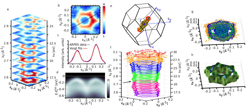
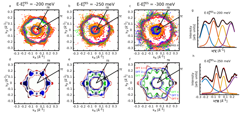
Constant energy surfaces (CESs) of are constructed below the VB maximum 43; 44; 45; 42. They are compared with CESs from DFT calculations, which require periodic boundary conditions, i.e., a distinct order within the Ge/Sb/Vc layer. We have chosen the cubic Petrov phase (Fig. 1d) to represent the metastable ABC stacking of the rock salt structure employing chemically pure Sb, Ge and Vc layers 30; 39. Since the corresponding DFT BZ is reduced in direction by a factor of with respect to the disordered rock salt phase (Fig. 1a-c), the ARPES data have to be back-folded into a range of Å-1 for comparison. Therefore, the measured data are divided into parts covering Å-1 each (see color code in Fig. 2f) and projected accordingly. Results at meV are shown in Fig. 2g, where each MDC has been fitted by four Voigt peaks as exemplary shown in Fig. 3g. The qualitative agreement with the DFT CESs (Fig. 2h) is reasonable, in particular, for the outer hexagon. Such agreement is also found at other energies as shown in Fig. 3a-f, where the different values are projected to the plane. However, quantitative differences are apparent as discussed in Supplementary Note 1.
Effective charge carrier density from ARPES and magnetotransport
Next, we deduce the effective charge carrier density from the detailed mapping of the VBs by ARPES. Since the VB maximum is found 105 meV below (Fig. 2d), one might conjecture the absence of a Fermi surface, i.e., , at least close to the surface, i.e., at the origin of the ARPES signal. However, the bands are significantly broadened, such that their tails cut (Fig. 2). Hence, the tails of the VB give rise to a non-vanishing . Accordingly, we replace the usual
| (1) |
where the Fermi volume includes all occupied states, with:
| (2) |
The integral covers the whole BZ and includes the weight of each state above (inset of Fig. 4a) according to
| (3) |
Here, is the fitted EDC peak at of band , after normalizing its area to unity.
Figure 4a shows an exemplary EDC (black points) fitted with two Voigt peaks (blue and green line), which are multiplied by the Fermi distribution function at K (thin, red line). This provides an excellent fitting result (thick red line). The weights of the two peaks above are evaluated to be % and % (inset of Fig. 4a) (methods). Generally, we find % for 97 % of the EDCs, where the largest are coincident with the maxima of . This is illustrated in the inset of Fig. 4d showing and for the EMC of Fig. 4b.
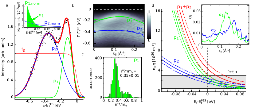
We only evaluate the contributions of the two upper VBs (, ), since all other bands are more than 1 eV below . Then, the for different are summed up and multiplied by in order to compensate for the part of the BZ, which is not probed by ARPES. Finally, we normalize appropriately. This eventually leads to with uncertainty resulting from the individual error bars of peak energies and peak widths within the Voigt fits. Taking only the contributions from the upper peak , we get . Since the surface might be influenced by band bending, we also calculated for an artificially varying with respect to the measured as displayed in Fig. 4d.
Next, we compare these with the results from Hall measurements, which yields the bulk charge carrier density (: Hall conductivity, : magnetic field) varying between and for nominally identical samples (table 3, methods). The variation is probably caused by the known, strong sensitivity of GST transport properties to disorder 17. The temperature dependence of is small within the interval K (changes %) demonstrating metallic conductivity. The interval of the data is marked in Fig. 4d. The larger excellently match , while the smaller ones are compatible with an shifted further upwards. In any case, the tails of the VB provide enough density of states to host the charge carrier density . We conclude that of GST-225 is indeed well above the VB maximum. In turn, we can estimate the required to locate at the VB maximum ( meV) to be (), i.e., an order of magnitude larger than the highest values found by the Hall measurements. This excludes a significant downwards band bending of the VB towards the surface.
In principle, one could argue that the peak width is not due to disorder, but due to the finite lifetime of the photo-hole produced by ARPES 43; 44. However, the Voigt fits, which add up a Gaussian peak and a Lorentzian peak, exhibit, on average, 99 % (97 %) Gaussian contribution and 1 % (3 %) Lorentzian contribution for (). Therefore, the lifetime broadening, encoded in the Lorentzian part, is negligible 43; 44. Moreover, the average electron scattering time detected by magnetotransport reasonably fits to the disorder induced peak widths (see below).
Electron mean free path from ARPES and magnetotransport
| (nm) | |||
|---|---|---|---|
| 1.04 |
Next, we deduce the average scattering lifetime of the electrons () and the average mean free path from the combination of ARPES and magnetotransport. In Supplementary Note 2, we show that the longitudinal conductivity and can be straightforwardly related to for an isotropic, M-shaped parabolic band in direction with negligible dispersion in direction and without peak broadening. Thus, in line with the ARPES data, we approximate the dispersion as
| (4) |
with being the cusp of the inverted parabola and representing the curvature in radial in-plane direction. This is different from a universal effective mass of the VB, since the band curvature differs for other directions. We obtain (Supplementary Note 2):
| (5) | |||||
| (6) |
with being distinct by a factor of from the standard Drude result, which is only valid for an isotropic, parabolic band centered at . To determine , we have, hence, to deduce from ARPES, besides . Corresponding parabolic fits to , exemplary shown in Fig. 4b, are executed for all EMCs at different azimuths in (, ) direction and different . This leads to the histogram of values in Fig. 4c with mean (: bare electron mass, table 1).
During the same fit, we naturally get an average as given in table 1 () and an average being meV. With the determined , we can use magnetotransport data and eq. 5 to estimate . For the sample, where fits best to from ARPES (table 3, methods), we measured and (at 300 K) leading to fs (table 2). The variation between different samples grown with the same parameters (methods, table 3) is negligible.
Straightforwardly, we can determine other parameters of the dispersion of eq. 4 including the Fermi wave vector and the Fermi velocity , while still neglecting the peak broadening (Supplementary Note 2):
| (7) | |||
| (8) | |||
| (9) | |||
| (10) | |||
| (11) |
where nm (table 1) is the length of the unit cell of the metastable rock salt phase (structure model in Fig. 1ac) perpendicular to the layers. The numerical values are again given for the sample with and (methods, table 3). is located in the band belonging to for all of our samples. Note that neither , as usual, nor , as typical for two-dimensional (2D) systems 47, enters the evaluation of , but only does. This reflects the dominating 2D-type dispersion for GST-225.
We also used a more refined, numerical calculation, which considers the variation of across the BZ and the peak broadening, i.e., the fact that is above the VB maximum, explicitly. Therefore, we use the low-temperature limit of Boltzmann’s relaxation model. We assume that the scattering time does not depend on and band index , reading which leads to
The group velocity is determined from the ARPES data as with the derivative taken at and not at . Since the results now depend critically on , we restrict the analysis to the sample with as used in eq. 7. Numerically, we obtain fs, which is nearly a factor of two smaller than within the simplified calculation. By the same numerical weighting, we determine the average group velocity at as leading to nm (table 2).
| Simple model | Full model | |
|---|---|---|
| in fs | ||
| in | ||
| in nm |
We compare the results of the refined model and the simplified model (eq. 5, 7) in table 2 revealing that the simplified model returns reasonable values, but deviates from the more exact, refined model by up to 40 %. This must be considered for the interpretation of magnetotransport data, where eq. 5 and 7 provide only reasonable estimates for , , , and with an intrinsic error of about 40 %.
Finally, we comment on the peak width, which is, on average, eV (FWHM) for the band . This can be compared with (Supplementary Note 3). We find fs in excellent agreement with fs as deduced from the transport data of the sample with highest conductivity (largest ) (table 2). This corroborates the assignment of the peak widths to disorder broadening, as already conjectured from its dominating Gaussian shapes. The fact that increases by only 15 % between room temperature and K 20 additionally shows that is dominated by disorder scattering. We conclude that disorder broadening is responsible for the peak widths within the spectral function of the upper valence band of GST-225. The relatively large peak widths (0.2 eV) allows the Fermi level to be well above all peak maxima, i.e., the charge carrier density fits into the tails of the bands. We finally stress that the peak broadening is not the origin of the p-type doping, which has been found previously to be dominated by excess vacancy formation 48; 49.
In-gap surface state
Motivated by our previous finding, that an M-shaped VB with maxima away from high symmetry points is only compatible with DFT calculations of GST exhibiting nontrivial topology 39, we searched for a surface state within the fundamental band gap. We found such a state by two-photon ARPES (2P-ARPES) exhibiting a linear, largely isotropic dispersion as well as helical, circular dichroism. The state is probably connected to a strongly spin-polarized state at the VB maximum revealed by spin polarized ARPES (S-ARPES).
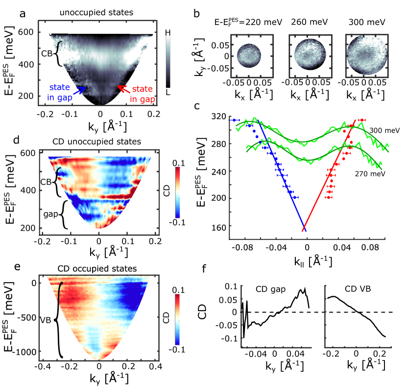
Optical measurements revealed a band gap of GST-225 of eV in rough agreement with DFT data 50, which was recently corroborated by scanning tunneling spectroscopy ( eV) 39; 51; 52. Hence, we have to probe this energy interval above the VB maximum, which does not contain bulk states. We employed laser-based 2P-ARPES at pump energy eV and probe energy eV, hence, populating states in the bulk band gap and in the lower part of the conduction band by the pump, which are subsequently probed by ARPES using the probe pulse. The time delay ps is chosen to optimize the contrast of the states within the bulk band gap. The EMC in Fig. 5a reveals a strong band above meV, which we attribute to the bulk conduction band (CB) at 450 meV above the VB maximum. Below this CB, a mostly linearly dispersing band faintly appears (arrows). Corresponding CECs (Fig. 5b) exhibit a largely circular structure of this band in the plane increasing in diameter with increasing energy. The linear dispersion of the band is deduced by applying two Voigt fits to each MDC as shown for two examples in Figure 5c. The resulting (points), averaged along and , are fitted using (red and blue line). This reveals a presumable band crossing at meV and a band velocity .
Due to the relatively strong one-photon background (methods), we could not evaluate the 2P-ARPES signal at lower , such that the presumable crossing point was not probed directly. However, all signatures of this band are compatible with a TSS with mostly linear dispersion.
In addition, we probed the circular dichroism (CD) by 2P-ARPES using a linearly polarized pump and a circular polarized probe pulse 53. The CD intensity is the scaled difference of photoelectron intensity after clockwise and counterclockwise circular polarization of the probe. It is known that the CD cannot be directly assigned to a spin polarization of initial states,32 but is likely related to an interplay of spin and orbital textures 54. In our case, it shows a sign inversion with the sign of (Fig. 5d). The opposite inversion is found within the CB and the upper VB, the latter probed by CD measurements of conventional ARPES (Fig. 5e). The same sequence of CD inversions between VB, TSS, and CB has been found for the prototype strong topological insulators Bi2Se331, Bi2Te3 32; 31, and Sb2Te3 33, which is an additional hint that the linearly dispersing state within the bulk band gap is a TSS.
Another fingerprint of non-trivial surface states is spin polarization 55; 56; 57. Such spin polarized surface states have been predicted by DFT calculations of the cubic Petrov phase of GST-225, in particular, a TSS traversing the band gap and a Rashba-type surface state at … meV 39. To this end, we probe the spin polarization of the occupied states at a selected pair of in-plane wave vectors (Fig. 6). We choose eV such that the CEC of the bulk VB is large in diameter (Fig. 2f), thereby increasing the possibility to probe a surface state in the inner part of the BZ, where DFT of the cubic Petrov phase predicted the presence of a TSS 39. Moreover, we used Å-1, large enough to avoid overlap of intensity from and , thereby getting along with the typically reduced angular resolution of S-ARPES. Indeed, we find strong in-plane spin-polarization of 40 % close to (Fig. 6b,c). The spin polarization inverts sign with the sign of the in-plane wave vector and is perpendicular to within error bars (Fig. 6c,d). The other spin polarized state at lower … eV might be related to the Rashba state mentioned above, which has similarly been found, e.g., for Sb2Te3(0001) 58.
The peak energy of the spin polarized state close to is meV (Fig. 6b), i.e., very close to the VB maximum, such that likely the spin-polarized state extends into the band gap. The error mostly comes from the different peak energies at and . We cannot prove that this state is connected to the linearly dispersing state of Fig. 5, which would hit the VB maximum at Å-1, if perfectly linear in dispersion down to the VB , but we believe that this is likely.
One might ask why such a linearly dispersing state is not observed in the one-photon ARPES data. A possible explanation is the fact that a surface state will follow the roughness of the surface, which for our films amounts to angles of 0.5 3∘ according to atomic force microscopy 39.
Assuming, for the sake of simplicity, the same state dispersion on all surfaces, this results in a broadening of the surface state by for eV. The widths of the 2P-ARPES peaks in Fig. 5c is and, hence, well compatible with this analysis. Since the bulk states are not influenced by this broadening mechanism, it gets rather difficult to discriminate the TSS in the presence of bulk VB states at similar as within our one-photon ARPES data.
We did not reproduce the dispersion of the found state in the bulk band gap by the DFT calculations of slabs of the cubic Petrov phase, which revealed a less steep dispersion of its TSS and another 39. We ascribe this discrepancy to the known, strong sensitivity of the TSS to details of GST’s atomic structure 34; 35; 36; 37; 38; 39. However, besides these remaining questions, both, the strong spin polarization close to the VB maximum and the linear dispersion within the bulk band gap are compatible with a TSS. This corrobarates the previous conjecture of a topologically inverted band structure of metastable GST-225 39.
Possible contribution of the topological surface state to conductivity
The possible presence of a TSS at , naturally protected from backscattering 55; 56; 57, raises the question whether it would contribute significantly to the conductivity. To answer this, we firstly compare the charge carrier density of the presumable TSS with the measured charge carrier density of the epitaxial film, after projecting to 2D according to (: film thickness). The latter varies between (film of largest conductivity) and (table 3, methods). For the non-degenerate 2D band of a linearly dispersing TSS, we have47:
| (14) |
A reasonable assumption for results from extrapolating the fitted linear dispersion of Fig. 5(c) to leading to . An upper estimate is , i.e., the value of the spin polarized state at the VB maximum. Hence, we get , respectively .
Comparing with the sample exhibiting (), is more than an order of magnitude larger than . We conclude that the charge carrier density is dominated by the bulk VB.
However, the mobility of a TSS () could be much larger than the mobility of the bulk VB (). Such a TSS conductivity dominates, if (: charge carrier density in the bulk VB after 2D projection). Within the two band model, we have 47
| (15) | |||||
| (16) |
We evaluate these equations for the sample with () using the assumption of a linearly dispersing TSS down to (). We solve eq. 15 and for the three remaining unknowns (, , ) leading to . The threshold for dominating is even lower for the other samples (table 3, methods). We moreover assume that only the surface contains a highly mobile TSS. In turn, the threshold for dominating has to be divided by two, if the interface to the Si(111) contains a TSS with the same and . For comparison, the record mobilities found for TSS in other systems (Bi2Se3, BiSbTeSe2) are 40; 41, i.e., significantly larger than the threshold.
We conclude with the encouraging possibility to prepare highly mobile, metastable GST-225 films, noting that polycrystalline films exhibit 22, which is an order of magnitude lower than for our best epitaxial film. Thus, one might boost the GST-225 conductivity by the combination of epitaxial films and adequate interface design leading to optimized TSS mobility 40; 41. This could be exploited within innovative devices combining the fast 7; 8 and energy efficient 9 phase change with ultrahigh mobility of the on-state.
Summary
We have mapped the 3D electronic bulk band structure close to of epitaxial GST films in the metastable rock salt phase and have correlated the results with magnetotransport data of identically prepared samples. The constant energy surfaces of the valence band close to are hexagonal tubes with little dispersion along , the direction perpendicular to the chemically distinct layers. The valence band maximum is about 100 meV below , such that only the tails of the disorder broadened states contribute to the conductivity. This is in line with the measured charge carrier densities from Hall measurements. We use the mapped band structure in combination with magnetotransport to determine the elastic scattering time (3 fs) and the mean free path (0.4 nm), the former being compatible with the peak widths found in ARPES.
Our detailed modeling reveals that variations of the band structure across the BZ. i.e., different band curvatures and peak broadenings, modify the deduced scattering time and average mean free path by about 40 %, such that simplified models, as typically used for the interpretation of magnetotransport data, cannot provide a better accuracy.
Besides, we find a linearly dispersing state within the bulk band gap which might have a topological origin. We estimate that this state would dominate the longitudinal conductivity at a mobility above , which is lower than the best mobilities of topological surface states so far () 40; 41. Currently, topological conductivity is not expected to be dominant, but by surface or interface optimization one might exploit it in future GST devices providing an ultrahigh mobility on-state.
Methods
Sample preparation. The GST films are grown by MBE at base presure Pa on a Si(111) substrate using elementary sources of Ge, Sb and Te and a substrate temperature of C. The growth rate was and the pressure increased to Pa during growth. XRD reveals that the films grow epitaxially in the single crystalline, metastable rock salt phase with [111] surface. The surface is Te terminated as evidenced by DFT calculations (not shown). The film thickness is determined by XRD fringes or by X-ray reflectometry to be 25 nm, 18 nm, and 13 nm for the samples used for ARPES, 2P-ARPES and S-ARPES, respectively. Twin domains are found, i.e., adjacent areas of ABC and CBA stacking of the hexagonal layers 39. A peak indicating the formation of a vacancy layer is observed by XRD, hinting to more ordered samples than in the purely disordered rock salt phase 20. The XRD data recorded after the ARPES measurements show variations in the (222) peak position by up to 1.5 % 20 and in the height of the vacancy layer peak by 15-25 %. However, the ARPES data of these samples are quite similar, i.e., peak positions of the VB vary by less than the peak widths. Samples are transferred in UHV between the MBE and the three different, analyzing ARPES systems using a UHV shuttle with background pressure of mbar. This prevents oxidation and surface contamination as cross-checked by x-ray photoelectron spectroscopy (XPS), such that no further preparation steps are required. The UHV transfer is crucial, since surface oxidation starts already at Pas of O2 29.
Photoelectron spectroscopy. The ARPES measurements of the valence band are recorded at a sample temperature K at BESSY II (beam line UE112-lowE-PGM2 ()) using a Scienta R8000 analyzer with energy resolution 20 meV and angular resolution . Linearly p-polarized light with photon energies eV and an incidence angle of is applied, which enabled a three-dimensional mapping of the band structure in momentum space (, , ). The Fermi energy of the ARPES setup has been determined on polycrystalline Cu with 5 meV precision.
The data set contained pixels, i.e., 998 different photoelectron energies , 666 different azimuthal angles , 49 polar angles , and 29 photon energies . The energy interval eV, eV] is used for background subtraction for each energy distribution curve (EDC) at a particular (, , ). Subsequently, the data are smoothed along and by a 5-point averaging. Accordingly, the data set is reduced to pixels. Finally, all EDCs are scaled to the same average value for each (, , ).
In order to deduce band centers of band , MDCs and EDCs at constant are extracted from the data and fitted by two or four Voigt peaks with variable intensities, widths, and relative contributions of the Gaussian and the Lorentzian. This leads to an excellent fit quality with negligible residuals as exemplarily shown in Fig. 2c, Fig. 3g-h, and Fig. 4a. The resulting up to four of MDC fits are then attributed to the preselected , respectively, the resulting of EDC fits are attributed to the preselected values. The resulting curves deduced from the two methods vary by Å-1, respectively, by meV, except for extreme values (see main text). The small deviations contribute straightforwardly to the error of the determined effective charge carrier densities and curvature parameters (Fig. 4).
Displaying the upper at selected for different , as shown for energy in Fig. 2f, consistently reveals a minimum diameter of the resulting constant energy lines at eV. Since DFT finds the minimum diameter of the upper VBs at the BZ boundary (e.g., Fig. 2h), we assume that the minimum at eV corresponds to the BZ boundary in direction.
This assumption is used to determine the inner potential with respect to the vacuum level for the final state electrons in the crystal
according to .
Restricting between 10 eV and 25 eV leaves us with the only possibility of eV. However, if the minimum diameter is in the center of the BZ, we would get eV. Since these differences are not important for our main conclusions, we select the most reasonable assumption that the smallest diameter is at the BZ boundary.
Using the inner potential, we calculate according to . For the CECs and CESs in Fig. 2, we use an average value of to relate to .
The ARPES data cover only 80 % of the BZ , i.e., a small part in direction is missing (Fig. 2e). This is due to the fact, that at lower and higher , the ARPES intensity drops drastically, such that fits become unreliable. However, in line with the DFT results, we do not believe that the hexagons change strongly within the remaining 20 %.
Fit procedures and fit errors All peaks of MDC and EDC curves are fitted by several Voigt peaks, i.e., by a combination of a Gaussian and a Lorentzian peak with the same maximum each. Comparing the results of MDC fits and EDC fits for energies below the VB maximum reveals only small differences between deduced values by or 10 meV on average, except for the extreme cases and (). The small discrepancies set a lower bound for error margins.
In order to extract from the fitted peaks of EDCs, the peak areas of () are normalized to one leading to , from which we evaluate the relative part of the peaks above (inset of Fig. 4a), being , the unoccupied percentage of the corresponding state.
The error of is only slightly smaller than the error of individual , being 5 % on average, which is due to the considerable variation of across the BZ (Fig. 4c). The deviation of individual curves from the parabola is negligible (Fig. 4b), i.e., the average energy distance of individual from the parabola ( meV) is less than the average fit error from the determination of by Voigt fits ( meV).
Spin polarized photoelectron spectroscopy. Spin resolved ARPES measurements are conducted at BESSY II, too, using the electron analyzer SPECS PHOIBOS 150 and linearly p-polarized synchrotron radiation at eV and incidence angle at K, providing an energy resolution of 100 meV and an angular resolution of . Spin analysis is performed with a Rice University Mott polarimeter operated at 26 kV resulting in a Sherman function of .
Two photon photoelectron spectroscopy. Angle-resolved bichromatic 2P-ARPES and additional, conventional ARPES experiments are conducted using the first, third and fourth harmonic of a titanium:sapphire oscillator, i.e., eV, eV, and eV, within a home-built setup 59; 53. The repetition rate of the laser is 80 MHz and the pulse length is 166 fs. The beam is initially p-polarized with an incidence angle of . The photon energy eV is used for the pump pulse followed by the probe pulse at eV, which hits the sample at a time delay after the pump. Due to time restrictions, of the probe pulse has not been changed such that we probe only a single . The photon energy eV is used for conventional ARPES to cross check the results obtained at BESSY II. Circular polarization, necessary for circular dichroism (CD) experiments, is obtained using a wave plate. Two-dimensional momentum distribution patterns at constant are recorded using an ellipsoidal ’display-type’ analyzer exhibiting an energy and angular resolution of meV and , respectively 60; 53. The work function of GST-225 turned out to be eV leading to a strong one-photon photoemission background from the probe pulse. In order to discriminate 2P-ARPES data from this background, the intensity of measurements at ps is subtracted from the data recorded at ps. Subsequently, the data are normalized to compensate for inhomogeneities of the channel plates. CD intensity displays the difference of photoelectron intensity using clock wise and counterclockwise polarized probe pulses divided by the sum of the two intensities.
Magnetotransport. Magnetotransport measurements are performed ex-situ. Since Hall measurements require insulating substrates while ARPES requires a conducting sample, the Hall data are from samples with lower substrate doping, but grown with identical parameters. After growth they are capped by Te to protect from oxidation. The samples are cut in square shapes of and, after decapping by a HF dip, are contacted by In and Au bond wires in a four-contact van der Pauw geometry. Magnetotransport measurements are conducted at K, current mA, and magnetic field T perpendicular to the surface. This leads to charge carrier densities and longitudinal conductivities as displayed in table 3 for K. It is likely that the upper 5 nm of the sample are oxidized 29; 61; 62 resulting in a systematic error of 25 % . We find a relatively broad statistical distribution of and , but due to correlations between the two values, the variation of the mobility is relatively small.
| (nm) | |||
|---|---|---|---|
| 0.13 | 2.700 | 0.0013 | 19 |
| 0.26 | 4.000 | 0.0010 | 28 |
| 3.0 | 60.000 | 0.0012 | 23 |
Band structure calculations. Density functional theory (DFT) calculations are performed within the generalized gradient approximation. We employ the full-potential linearized augmented plane-wave method in bulk and thin-film geometry as implemented in the FLEUR code. According to Ref. 30, the Petrov stacking sequence (Te-Sb-Te-Ge-Te-Vc-Te-Ge-Te-Sb-) 15 is assumed for the metastable rock salt phase by tripling the Petrov-type unit cell containing 10 layers in order to realize the ABC stacking of the rock salt phase (Fig. 1d). The resulting BZ of the unit cell of 30 layers, is a factor of five smaller in direction ( Å-1) than the BZ of the disordered metastable rock salt phase, relevant for the ARPES data ( layers in a unit cell, Fig. 1c). Hence, we use fivefold backfolding of the experimental data (Fig. 2g) to compare with the DFT data (Fig. 2h).
Additional DFT calculations are performed for disordered slabs (Fig. 1b) with methodology otherwise similar to Ref. 63. We simulate maximum disorder by occupying each cationic plane randomly with Ge:Sb:Vc in a 2:2:1 ratio. These planes are parallel to the (111) surface, and include the disordered subsurface layer, whereas the surface itself is terminated by Te 63. Different structure models of the cationic plane were randomly generated, and after relaxation showed a standard deviation of 3 meV/atom in total energies. The computed surface energies range from 12 to 17 meV Å-2 in a Te-poor environment, which can well be reconciled with previous results for ideally ordered GST 63.
More details including atomic coordinates are given in Supplementary Note 4.
Acknowledgements.
We gratefully acknowledge helpful discussions with H. Bluhm, M. Wuttig, and C. M. Schneider as well as financial support by the German Science Foundation (DFG): SFB 917 via Project A3, SPP 1666 (Topological Insulators) via Mo858/13-1, and Helmholtz-Zentrum Berlin (HZB). V.L.D. was supported by the German Academic Scholarship Foundation. Computing time was provided to G.B. by the Jülich-Aachen Research Alliance (JARA-HPC) on the supercomputer JURECA at Forschungszentrum Jülich.Author contributions
M.M. provided the idea of the experiment. J.K., M.L. and C.P. carried out all (S)ARPES experiments under the supervision of E.G., J.S-B., O.R., and M.M.. S.O., J.K., P.K., and P.B. performed the 2P-ARPES measurements under the supervision of T.F.. J.E.B., R.N.W., S.C., and V.B. grew the samples via MBE, supervised by R.C.. V.B. performed the electrical transport measurements also supervised by R.C.. G.B. provided the DFT calculations for comparison to the ARPES data. V.L.D. and R.D. performed the additional DFT modelling of the disordered, metastable surfaces. M.L., J.K, and S.O. evaluated the experimental data. M.L., M.M., and J.K. derived the models for the interpretation of the data as discussed in the manuscript. M.M., M.L. and J.K. wrote the manuscript containing contributions from all co-authors. The authors declare no competing financial interests.
Supplementary Note 1: Comparison between ARPES data and DFT data of the cubic Petrov phase
| meV | meV | meV | ||||
|---|---|---|---|---|---|---|
| Direction | ||||||
| ARPES I | ||||||
| DFT 1 | ||||||
| DFT 2 | ||||||
| DFT 3 | ||||||
| ARPES II | ||||||
| DFT 4 | ||||||
| DFT 5 | ||||||
| DFT 6 | ||||||
As visible in Fig. 3 of the main text, there are differences between DFT and ARPES results. Besides the mostly excellent fit quality of the ARPES data (Fig. 3g-h), there are more distinct bands in the DFT calculation (red, blue and green contours), which we tentatively attribute to the higher degree of order in the cubic Petrov phase with respect to the more disordered rock-salt phase probed by ARPES. The different bands in DFT can be attributed mostly to Sb p-states with different nodal structure along the large unit cell of the Petrov phase in direction. We assume that these different bands are differently sensitive to the arrangement of the pure Sb layers, which are only present in the idealized Petrov phase, but not in the experiment. The resulting stronger dispersion along (of a hypothetical rock-salt BZ) even induces closed CESs between the tubes at higher (Fig. 3d), which are not observed in the experiment (Fig. 3a). Additionally, the inner constant energy surfaces (CESs) of the ARPES data and the DFT data are different. Corresponding values for the up to 6 different CESs from DFT and the 2 CESs from ARPES are shown in Supplementary Table 4. While the outer, experimental CES (ARPES I) reasonably fits with the outer DFT CESs (DFT ), the inner, experimental CES (ARPES II) is smaller than the corresponding DFT CESs (DFT ). Additionally, the values of DFT disperse more strongly with energy than for ARPES II, i.e., the experimental is steeper in (, ) direction. Again, we believe that these differences are caused by the additional order in the cubic Petrov phase, assumed for the DFT calculations.
Supplementary Note 2: Boltzmann relaxation model for an energy broadened M-shaped band
Summary of basic equations
The relation between electric field and current density in a two-dimensional solid (thin film) is:
| (17) |
where is the conductivity matrix.
Within Boltzmann’s relaxation model for a single spin degenerate band, one gets 64:
| (18) | |||||
| (19) |
Here, is the group velocity in current direction , is the relaxation time, is the Fermi distribution function, is the magnetic induction applied perpendicular to the (,) plane, and
| (20) |
where Fermi volume is the Fermi volume of the spin-degenerate band, i.e., the volume within the BZ, which is enclosed by the corresponding Fermi surfaces.
Taking the band broadening into account, we have to replace the selected energies by the more general binding energy and have to multiply the Fermi distribution function at with the normalized peak intensity at being , i.e.:
| (21) |
For the sake of completeness, we finally add the standard derivation of the Drude result at K, simplifying Supplementary Equation 18 to:
| (22) |
with the sum covering the possibly multiple Fermi surfaces of different spin degenerate bands, being the corresponding Fermi wave vector, and being the group velocity in the direction perpendicular to the Fermi surface. This ( K)-approximation is reasonably valid as long as , , and vary negligibly within an energy interval of around (: Boltzmann constant).
For a single, parabolic band with dispersion and the assumption that is independent of , one straightforwardly recovers the well-known Drude result:
| (23) |
Boltzmann model for the M-shaped valence band of GST-225
Neglecting the disorder broadening, the upper valence band of GST-225 found by ARPES can be reasonably fitted by:
| (24) |
with , i.e., an inverted, quadratic dispersion exhibiting rotational symmetry in the plane and no dispersion in direction. The cusp of the parabola is at and the curvature in radial in-plane direction is given by .
The resulting group velocities are:
| (25) | |||||
| (26) |
where the latter exploits the cylindrical shape of the Fermi surface.
Defining as the angle between and , i.e., , we get:
| (27) |
Averaging over all angles leads to:
| (28) |
Thus, Supplementary Equation 22 reads for independent of :
| (29) |
with being the radius of the Fermi cylinder. Thus, we are left with the task to determine the area of the two cylindrical Fermi surfaces of the M-shaped band:
| (30) |
with nm being the extension of the unit cell of the disordered rock-salt phase along the stacking direction of the layers (Fig. 1a, c of main text).46 Using , i.e., exploiting the symmetric parabolicity of the band, we get:
| (31) | |||||
Supplementary Note 3: Relation between scattering time and peak width
Generally, one can argue that the mean free path of an electron sets the limit for its continuous wave-type propagation. Hence, the electron wave function gets additionally structured on this length scale leading, e.g., to nodes at repulsive scatterers. This can be approximated by with a proportionality constant of order one, depending in detail on the potential shape of the scatterers and the effective dimension 65; 66. Here, describes the width of the peaks within the spectral function in momentum space. Using with group velocity and scattering time as well as , as valid for an isotropic in-plane movement as largely present in GST-225, we get straightforwardly by Taylor expansion:
| (35) |
Supplementary Note 4: Crystal structures for the DFT calculations
The cubic Petrov phase, as sketched in Fig.1d of the main text, is calculated using DFT in the generalized gradient approximation 67 with the full-potential linearized augmented planewave method 68. The structure is derived from the hexagonal Petrov phase by stacking three hexagonal unit cells and displacing them by with respect to each other in the [0001] plane. The resulting hexagonal unit cell has lattice parameters Å and Å and atomic positions as indicated in Supplementary Table 5.
| atom | ||||||
|---|---|---|---|---|---|---|
| Te | B | C | A | |||
| Ge | C | A | B | |||
| Te | A | B | C | |||
| Sb | B | C | A | |||
| Te | C | A | B | |||
| Sb | A | B | C | |||
| Te | B | C | A | |||
| Ge | C | A | B | |||
| Te | A | B | C |
The muffin-tin radii, , used in the calculations are Å for Te and Ge and Å for the Sb atoms. The basis-set cutoff was limited to and for the self-consistent calculations -points were used in the irreducible Brillouin zone. For the plotting of the CECs, the reciprocal space was sampled with -points. For the disordered surface models, a ZIP file provided additionally as Supporting Information contains the six structural models (in VASP CONTCAR format), exemplary input files (INCAR and KPOINTS) summarizing the parameters, as well as information on the particular pseudopotential files (POTCAR) employed for the computations.
References
- Wuttig and Yamada (2007) M. Wuttig and N. Yamada, Nat. Mater. 6, 824 (2007).
- Wuttig and Raoux (2012) M. Wuttig and S. Raoux, Z. Anorg. Allg. Chem. 638, 2455 (2012).
- Tominaga et al. (2013) J. Tominaga, A. V. Kolobov, P. Fons, T. Nakano, and S. Murakami, Adv. Mater. Interfaces 1, 1300027 (2013).
- Deringer et al. (2015) V. L. Deringer, R. Dronskowski, and M. Wuttig, Adv. Funct. Mater. 25, 6343 (2015).
- Ovshinsky (1968) S. R. Ovshinsky, Phys. Rev. Lett. 21, 1450 (1968).
- Yamada et al. (1987) N. Yamada, E. Ohno, N. Akahira, K. Nishiuchi, K. Nagata, and M. Takao, Jpn. J. Appl. Phys. 26, 61 (1987).
- Yamada et al. (1991) N. Yamada, E. Ohno, K. Nishiuchi, N. Akahira, and M. Takao, J. Appl. Phys. 69, 2849 (1991).
- Loke et al. (2012) D. Loke, T. H. Lee, W. J. Wang, L. P. Shi, R. Zhao, Y. C. Yeo, T. C. Chong, and S. R. Elliott, Science 336, 1566 (2012).
- Xiong et al. (2011) F. Xiong, A. D. Liao, D. Estrada, and E. Pop., Science 332, 568 (2011).
- Park et al. (2007) J.-B. Park, G.-S. Park, H.-S. Baik, J.-H. Lee, H. Jeong, and K. Kim, J. Electrochem. Soc. 154, H139 (2007).
- Matsunaga and Yamada (2004) T. Matsunaga and N. Yamada, Phys. Rev. B 69, 104111 (2004).
- Matsunaga et al. (2006) T. Matsunaga, R. Kojima, N. Yamada, K. Kifune, Y. Kubota, Y. Tabata, and M. Takata, Inorg. Chem. 45, 2235 (2006).
- Matsunaga et al. (2008) T. Matsunaga, H. Morita, R. Kojima, N. Yamada, K. Kifune, Y. Kubota, Y. Tabata, J.-J. Kim, M. Kobata, E. Ikenaga, and K. Kobayashi, J. Appl. Phys. 103, 093511 (2008).
- Silva et al. (2008) J. L. F. D. Silva, A. Walsh, and H. Lee, Phys. Rev. B 78, 224111 (2008).
- Petrov et al. (1968) I. I. Petrov, R. M. Imamov, and Z. G. Pinsker, Sov. Phys. Crystallogr. 13, 339 (1968).
- Kooi and Hosson (2002) B. J. Kooi and J. T. M. D. Hosson, J. Appl. Phys. 92, 3584 (2002).
- Siegrist et al. (2011) T. Siegrist, P. Jost, H. Volker, M. Woda, P. Merkelbach, C. Schlockermann, and M. Wuttig, Nat. Mater. 10, 202 (2011).
- Schneider et al. (2012) M. N. Schneider, X. Biquard, C. Stiewe, T. Schröder, P. Urban, and O. Oeckler, Chem. Commun. 48, 2192 (2012).
- Zhang et al. (2012) W. Zhang, A. Thiess, P. Zalden, R. Zeller, P. H. Dederichs, J.-Y. Raty, M. Wuttig, S. Blügel, and R. Mazzarello, Nat. Mater. 11, 952 (2012).
- Bragaglia et al. (2016a) V. Bragaglia, F. Arciprete, W. Zhang, A. M. Mio, E. Zallo, K. Perumal, A. Giussani, S. Cecchi, J. E. Boschker, H. Riechert, S. Privitera, E. Rimini, R. Mazzarello, and R. Calarco, Sci. Rep. 6, 23843 (2016a).
- Subramaniam et al. (2009) D. Subramaniam, C. Pauly, M. Liebmann, M. Woda, P. Rausch, P. Merkelbach, M. Wuttig, and M. Morgenstern, Appl. Phys. Lett. 95, 103110 (2009).
- Volker (2013) H. Volker, Disorder and electrical transport in phase-change materials, Ph.D. thesis, RWTH Aachen University (2013).
- Katmis et al. (2011) F. Katmis, R. Calarco, K. Perumal, P. Rodenbach, A. Giussani, M.Hanke, A. Proessdorf, A. Trampert, F. Grosse, R. Shayduk, R. Campion, W. Braun, and H. Riechert, Cryst. Growth Des. 11, 4606 (2011).
- Rodenbach et al. (2012) P. Rodenbach, R. Calarco, K. Perumal, F. Katmis, M. Hanke, A. Proessdorf, W. Braun, A. Giussani, A. Trampert, H. Riechert, P. Fons, and A. V. Kolobov, Phys. Status Solidi-R 6, 415 (2012).
- Bragaglia et al. (2014) V. Bragaglia, B. Jenichen, A. Giussani, K. P. H. Riechert, and R. Calarco, J. Appl. Phys. 116, 054913 (2014).
- Cecchi et al. (2017) S. Cecchi, E. Zallo, J. Momand, R. Wang, B. Kooi, M. Verheijen, and R. Calarco, APL Mater. 5, 026107 (2017).
- Mitrofanov et al. (2016) K. V. Mitrofanov, P. Fons, K. Makino, R. Terashima, T. Shimada, A. V. Kolobov, J. Tominaga, V. Bragaglia, A. Giussani, R. Calarco, H. Riechert, T. Sato, T. Katayama, K. Ogawa, T. Togashi, M. Yabashi, S. Wall, D. Brewe, and M. Hase, Sci. Rep. 6, 20633 (2016).
- Bragaglia et al. (2016b) V. Bragaglia, K. Holldack, J. E. Boschker, F. Arciprete, E. Zallo, T. Flissikowski, and R. Calarco, Sci. Rep. 6, 28560 (2016b).
- Yashina et al. (2008) L. V. Yashina, R. Püttner, V. S. Neudachina, T. S. Zyubina, V. I. Shtanov, and M. V. Poygin, J. Appl. Phys. 103, 094909 (2008).
- Sun et al. (2006) Z. Sun, J. Zhou, and R. Ahuja, Phys. Rev. Lett. 96, 055507 (2006).
- Wang and Gedik (2013) Y. Wang and N. Gedik, Phys. Status Solidi-R 7, 64 (2013).
- Scholz et al. (2013) M. R. Scholz, J. Sánchez-Barriga, J. Braun, D. Marchenko, A. Varykhalov, M. Lindroos, Y. J. Wang, H. Lin, A. Bansil, J. Minár, H. Ebert, A. Volykhov, L. V. Yashina, and O. Rader, Phys. Rev. Lett. 110, 216801 (2013).
- Seibel et al. (2015) C. Seibel, H. Maaß, H. Bentmann, J. Braun, K. Sakamoto, M. Arita, K. Shimada, J. Minár, H. Ebert, and F. Reinert, J. Electron Spectrosc. 201, 110 (2015).
- Kim et al. (2010) J. Kim, J. Kim, and S.-H. Jhi, Phys. Rev. B 82, 201312 (2010).
- Sa et al. (2011) B. Sa, J. Zhou, Z. Song, Z. Sun, and R. Ahuja, Phys. Rev. B 84, 085130 (2011).
- Kim et al. (2012) J. Kim, J. Kim, K.-S. Kim, and S.-H. Jhi, Phys. Rev. Lett. 109, 146601 (2012).
- Sa et al. (2012) B. Sa, J. Zhou, Z. Sun, and R. Ahuja, Europhys. Lett. 97, 27003 (2012).
- Silkin et al. (2013) I. V. Silkin, Y. M. Koroteev, G. Bihlmayer, and E. Chulkov, Appl. Surf. Sci. 267, 169 (2013).
- Pauly et al. (2013) C. Pauly, M. Liebmann, A. Giussani, J. Kellner, S. Just, J. Sánchez-Barriga, E. Rienks, O. Rader, R. Calarco, G. Bihlmayer, and M. Morgenstern, Appl. Phys. Lett. 103, 243109 (2013).
- Koirala et al. (2015) N. Koirala, M. Brahlek, M. Salehi, L. Wu, J. Dai, J. Waugh, T. Nummy, M.-G. Han, J. Moon, Y. Zhu, D. Dessau, W. Wu, N. P. Armitage, and S. Oh, Nano Lett. 15, 8245 (2015).
- Xu et al. (2016) Y. Xu, I. Miotkowski, and Y. P. Chen, Nat. Commun. 7, 11434 (2016).
- Medjanik et al. (2017) K. Medjanik, O. Fedchenko, S. Chernov, D. Kutnyakhov, M. Ellguth, A. Oelsner, B. Schönhense, T. R. F. Peixoto, P. Lutz, C.-H. Min, F. Reinert, S. Däster, Y. Acremann, J. Viefhaus, W. Wurth, H. J. Elmers, and G. Schönhense, Nat. Mater. 16, 615 (2017).
- Hüfner (2003) S. Hüfner, Photoelectron Spectroscopy (Springer, 2003).
- Matzdorf (1998) R. Matzdorf, Surf. Sci. Rep. 30, 153 (1998).
- Zhang et al. (2011) J. Zhang, C.-Z. Chang, Z. Zhang, J. Wen, X. Feng, K. Li, M. Liu, K. He, L. Wang, X. Chen, Q.-K. Xue, X. Ma, and Y. Wang, Nat. Commun. 2, 574 (2011).
- Nonaka et al. (2000) T. Nonaka, G. Ohbayashi, Y. Toriumi, Y. Mori, and H. Hashimoto, Thin Solid Films 370, 258 (2000).
- Ando et al. (1982) T. Ando, A. B. Fowler, and F. Stern, Rev. Mod. Phys. 54, 437 (1982).
- Edwards et al. (2006) A. H. Edwards, A. C. Pineda, P. A. Schultz, M. G. Martin, A. P. Thompson, H. P. Hjalmarson, and C. J. Umrigar, Phys. Rev. B 73, 045210 (2006).
- Wuttig et al. (2006) M. Wuttig, D. Lüsebrink, D. Wamwangi, W. Wełnic, M. Gilleßen, and R. Dronskowski, Nat. Mater. 6, 122 (2006).
- Lee et al. (2005) B.-S. Lee, J. R. Abelson, S. G. Bishop, D.-H. Kang, B.-K. Cheong, and K.-B. Kim, J. Appl. Phys. 97, 093509 (2005).
- Kellner (2017) J. Kellner, A surface science based window to transport properties: The electronic structure of Te-based chalcogenides close to the Fermi level, Ph.D. thesis, RWTH Aachen University (2017).
- Kellner et al. (2017) J. Kellner, G. Bihlmayer, V. L. Deringer, M. Liebmann, C. Pauly, A. Giussani, J. E. Boschker, R. Calarco, R. Dronskowski, and M. Morgenstern, Phys. Rev. B 96, 245408 (2017).
- Niesner et al. (2012) D. Niesner, T. Fauster, S. V. Eremeev, T. V. Menshchikova, Y. M. Koroteev, A. P. Protogenov, E. V. Chulkov, O. E. Tereshchenko, K. A. Kokh, O. Alekperov, A. Nadjafov, and N. Mamedov, Phys. Rev. B 86, 205403 (2012).
- Crepaldi et al. (2014) A. Crepaldi, F. Cilento, M. Zacchigna, M. Zonno, J. C. Johannsen, C. Tournier-Colletta, L. Moreschini, I. Vobornik, F. Bondino, E. Magnano, H. Berger, A. Magrez, P. Bugnon, G. Autes, O. V. Yazyev, M. Grioni, and F. Parmigiani, Phys. Rev. B 89, 125408 (2014).
- Hasan and Kane (2010) M. Z. Hasan and C. L. Kane, Rev. Mod. Phys. 82, 3045 (2010).
- Qi and Zhang (2011) X.-L. Qi and S.-C. Zhang, Rev. Mod. Phys. 83, 1057 (2011).
- Ando (2013) Y. Ando, J. Phys. Soc. Jpn. 82, 102001 (2013).
- Pauly et al. (2012) C. Pauly, G. Bihlmayer, M. Liebmann, M. Grob, A. Georgi, D. Subramaniam, M. R. Scholz, J. Sánchez-Barriga, A. Varykhalov, S. Blügel, O. Rader, and M. Morgenstern, Phys. Rev. B 86, 235106 (2012).
- Thomann et al. (1999) U. Thomann, I. L. Shumay, M. Weinelt, and T. Fauster, Appl. Phys. B 68, 531 (1999).
- Rieger et al. (1983) D. Rieger, R. D. Schnell, W. Steinmann, and V. Saile, Nucl. Instrum. Methods 208, 777 (1983).
- Zhang et al. (2010) Z. Zhang, J. Pan, Y. L. Foo, L. W.-W. Fang, Y.-C. Yeo, R. Zhao, L. Shi, and T.-C. Chong, Appl. Surf. Sci. 256, 7696 (2010).
- Gourvest et al. (2012) E. Gourvest, B. Pelissier, C. Vallee, A. Roule, S. Lhoutis, and S. Maitrejean, J. Electrochem. Soc. 159, H373 (2012).
- Deringer et al. (2012) V. L. Deringer, M. Lumeij, and R. Dronskowski, J. Phys. Chem. C 116, 15801 (2012).
- Ibach and Lüth (2009) H. Ibach and H. Lüth, Solid-State Physics (Springer, 2009).
- Kramer and MacKinnon (1993) B. Kramer and A. MacKinnon, Rep. Prog. Phys. 56, 1469 (1993).
- Evers and Mirlin (2008) F. Evers and A. D. Mirlin, Rev. Mod. Phys. 80, 1355 (2008).
- Perdew et al. (1996) J. P. Perdew, K. Burke, and M. Ernzerhof, Phys. Rev. Lett. 77, 3865 (1996).
- Wimmer et al. (1981) E. Wimmer, H. Krakauer, M. Weinert, and A. J. Freeman, Phys. Rev. B 24, 864 (1981).