Planar n-in-n quad module prototypes for the ATLAS ITk upgrade at HL-LHC
Abstract
In order to meet the requirements of the High Luminosity LHC (HL-LHC), it will be necessary to replace the current tracker of the ATLAS experiment. Therefore, a new all-silicon tracking detector is being developed, the so-called Inner Tracker (ITk). The use of quad chip modules is intended in its pixel region. These modules consist of a silicon sensor that forms a unit along with four read-out chips.
The current ATLAS pixel detector consists of planar n-in-n silicon pixel sensors. Similar sensors and four FE-I4 read-out chips were assembled to first prototypes of planar n-in-n quad modules. The main focus of the investigation of these modules was the region between the read-out chips, especially the central area between all four read-out chips. There are special pixel cells placed on the sensor which cover the gap between the read-out chips.
This contribution focuses on the characterization of a non-irradiated device, including important sensor characteristics, charge collection determined with radioactive sources as well as hit efficiency measurements, performed in the laboratory and at testbeams. In addition, first laboratory results of an irradiated device are presented.
1 ATLAS ITk upgrade
To cope with the increased luminosity, data rate and radiation damage at the HL-LHC [1], major upgrades of the ATLAS experiment [2] are foreseen [3, 4]. One upgrade will be the replacement of the current tracking detector. The proposed new inner tracker (ITk) [5] is designed to operate under conditions featuring an increased track density, following from approximately 200 inelastic proton-proton collisions per beam crossing, and a high radiation dose estimated from the expected integrated luminosity of 3000 fb-1 over ten years of operation.
The ITk will be an all-silicon tracker with five pixel and four strip layers in the central region, enclosed by end-caps with six strip disks and a number of pixel rings on each side [5]. Quad chip modules are foreseen in the outer layers and the rings of the pixel region. A quad module consists of four read-out chips which are bump bonded to one silicon sensor.
2 n-in-n quad modules
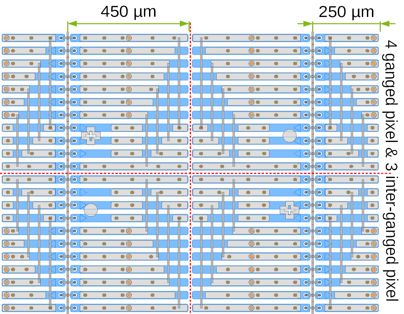
The two quad module prototypes presented here consist of oxygenated n-doped float zone silicon sensors which carry highly n-doped pixel implants with moderated p-spray isolation and a p-doped backside. The n-bulk thickness is 285 µm. This technology was selected since the current ATLAS pixel detector also consists of such planar n-in-n pixel sensors [6]. The pixels are connected to a front-end chip with the help of a flip-chip process employing tin-lead-bumps. The used FE-I4 front-end chip [7] was developed for the Insertable B-Layer (IBL) [8, 9] of the ATLAS experiment. It has a feature size of 130 nm resulting in µm2 pixel cells, arranged in 80 columns and 336 rows. Four FE-I4 chips with a bulk thickness of 700 µm are flip-chipped to one sensor. For technological reasons, two chips should not touch each other, which causes gaps in the horizontal and vertical directions. To cover the gap in the direction of the long pixel side between two read-out chips, two ‘long pixels’ are extended to a length of 450 µm in every row. To cover the gap in the direction of the short pixel side between two read-out chips, in every column four ‘ganged pixels’ are connected via a metal trace to four pixels without dedicated read-out channels, with three ‘inter-ganged pixels’ in-between. ‘Inter-ganged pixels’ are standard µm2 pixel cells with a dedicated read-out channel. Because they are enclosed by ‘ganged pixels’, they are treated separately. The layout of the sensor’s central region is shown in Figure 1, where the combination of these designs leads to special pixel cells like ‘long-ganged pixels’. To reduce inactive sensor area, the first and the last pixel column is shifted completely beneath the guard rings. These pixel columns are referred to as ‘edge pixels’.
If all these pixels are taken into account, the sensor consists of individual pixel cells with the external dimensions of mm2, resulting in a total sensitive area of 13.736 cm2.
Each quad module assembly is mounted on a PCB. Sensor and front-end pads were wire-bonded to allow calibration and read-out. The PCB thickness is 1.5 mm. It has four rectangular openings of cm2 in the middle of each read-out chip and an additional opening in the center of the sensor. After investigation in lab and testbeam measurements, one quad was irradiated at CERN-PS IRRAD [10] in a first step up to a fluence of ncm-2.
3 IV measurements
Current-voltage characteristics (IV curves) reveal important sensor properties and are also a main criterion for quality control. Certain acceptance criteria must be fulfilled by the sensors in order to be considered for the ITk. For unirradiated planar pixel sensors, the leakage current at 20 ∘C should be less than 0.75 µAcm-2 at the operating bias voltage. The breakdown voltage should be at least 20 V higher than the operating voltage. After irradiation to ncm-2, for a sensor of 150 µm thickness, the leakage current at -25 ∘C should be less than 20 µAcm-2 at 400 V, the breakdown voltage should be higher than 400 V.
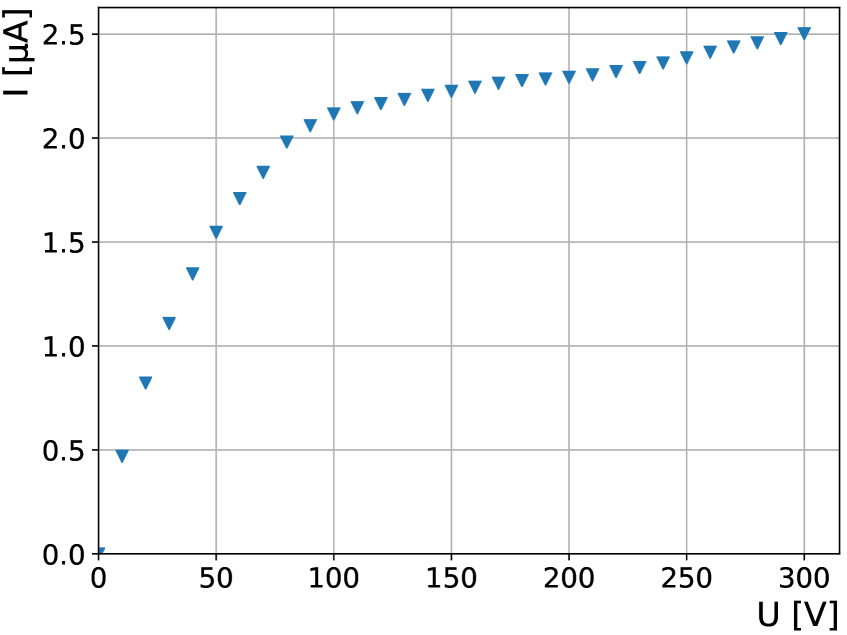
Before irradiation, the current was measured up to a maximum voltage of 300 V in a climate chamber at 20 ∘C. The diode-like curve is shown in Figure 3. At 100 V, where the plateau starts, a current of 2.1 µA is measured. The slope is determined to be 1.9 nAV-1. Thus, the acceptance criteria are fulfilled, the current is far below the 10.3 µA requested for a sensor with an area of 13.7 cm2 and no breakdown occurs.
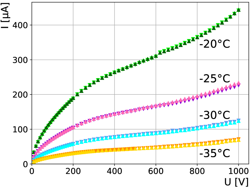
After irradiation, the maximum voltage was increased to 1000 V. Measurements were performed at multiple temperatures in a climate chamber. To ensure reproducibility, a second curve was recorded immediately after the first. As shown in Figure 3, again no breakdown occurred. Since only a fluence of ncm-2 was investigated, no statement about the acceptance criteria can be made. The given temperature corresponds to the set temperature of the climate chamber. An offset in sensor temperature caused by self heating is expected but not taken into account.
The humidity inside the climate chamber was controlled and kept low by its circuit, but it was not monitored.
4 Tuning of front-end chips
Each pixel read-out cell of the FE-I4 chip contains a discriminator with an adjustable threshold. If a signal in the sensor exceeds this threshold, the time over threshold (ToT) is measured. This ToT is therefore directly related to the induced charge in the sensor. The threshold value and the ToT response at an injected reference charge can be adjusted by various DACs. This is necessary to guarantee homogeneous responses under different conditions because the FE-I4 electronics are susceptible to influences such as temperature and radiation. The procedure of adjusting the response of all pixels is called tuning.
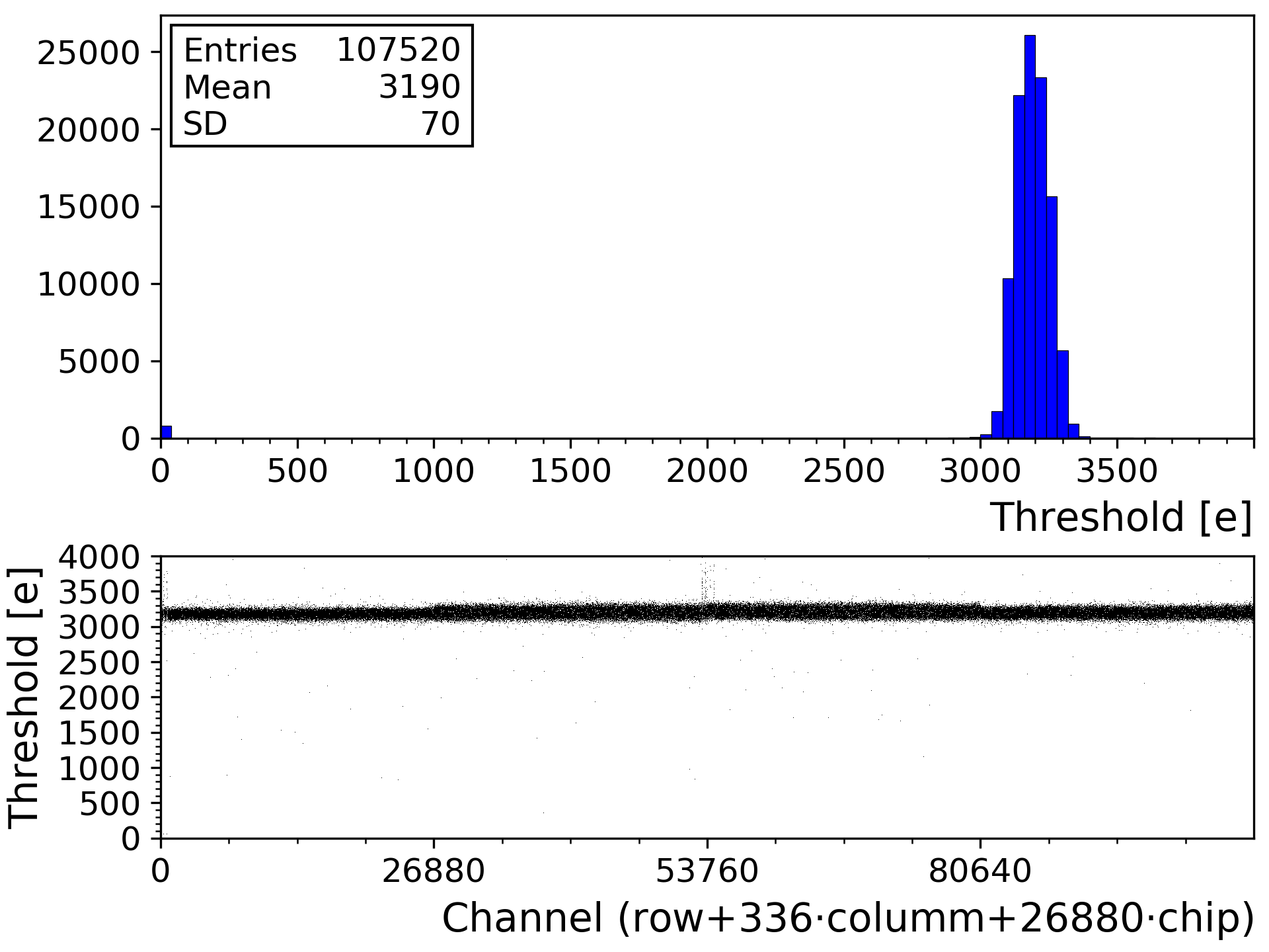
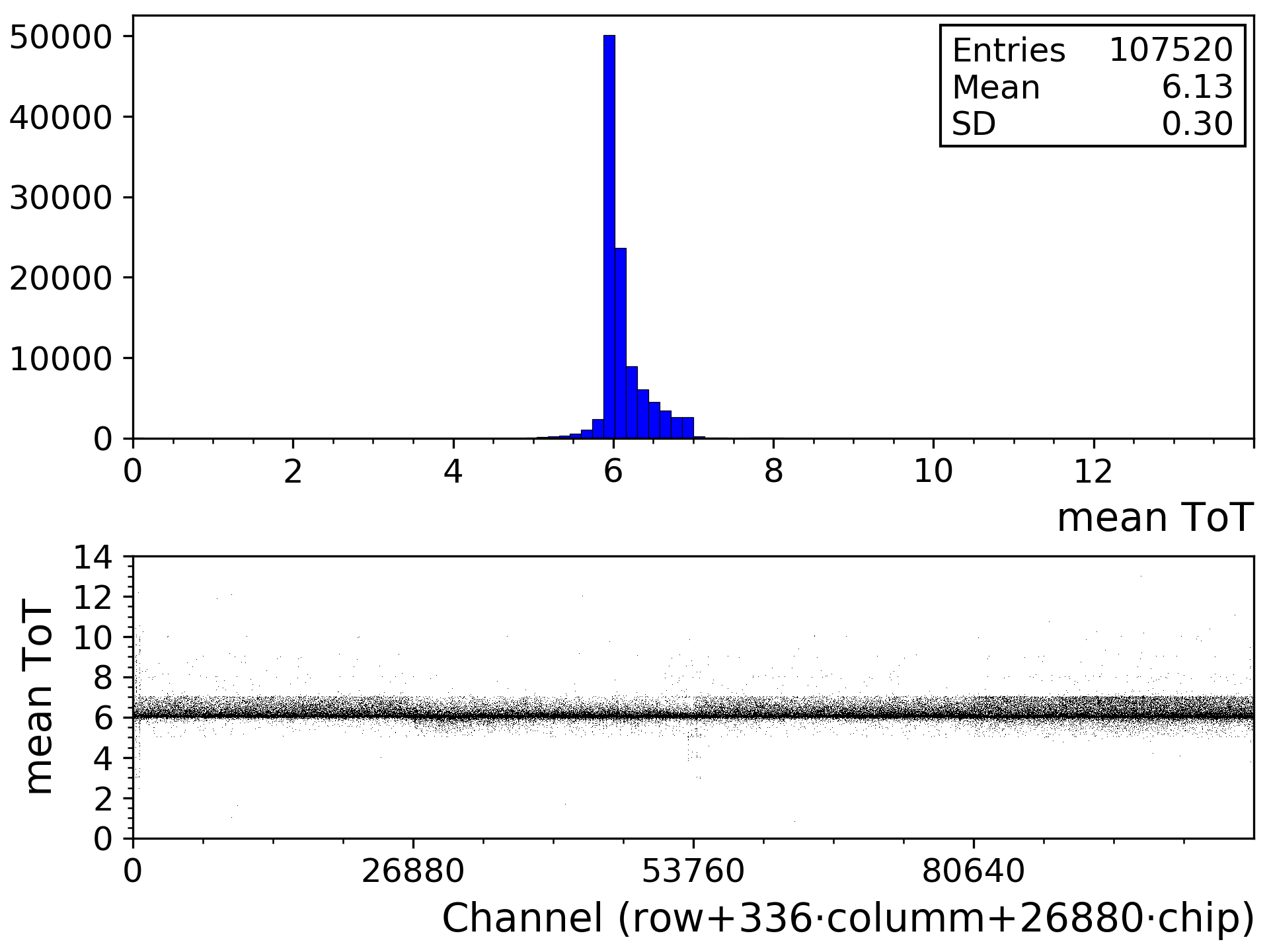
Before irradiation, measurements were performed using a tuning with a threshold of e and a response of ToT units at a reference charge of 20 ke. The results for the tuning used for measurements after irradiation are a threshold of e and a response of () ToT units at a reference charge of 20 ke. These distributions are shown in Figure 4.
5 Source measurements
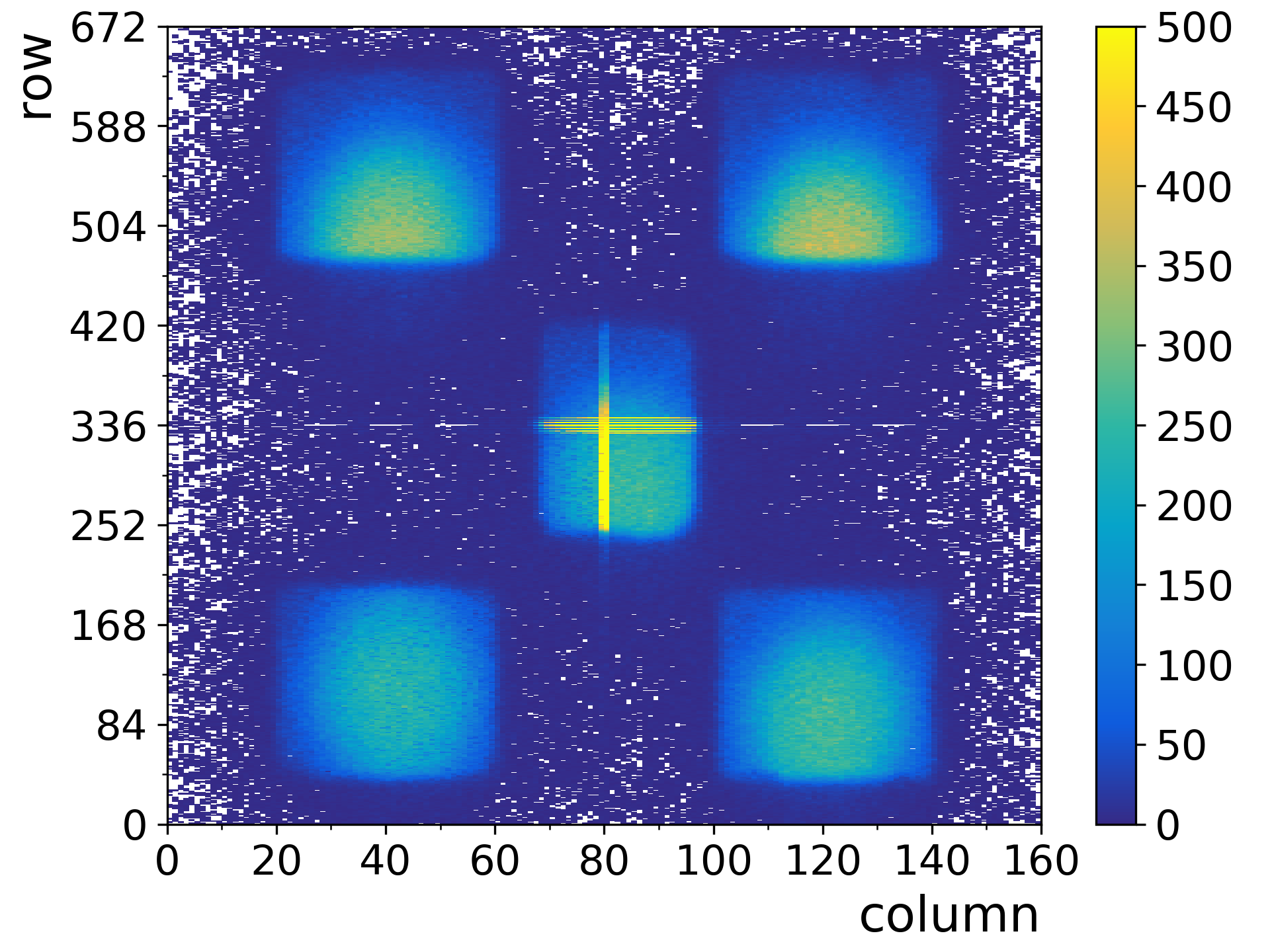
Before irradiation, measurements were performed with a Sr-90 source. Emitted -particles pass through the sensor, the read-out chip, the PCB or its openings and are finally detected in a scintillator, which sends a read-out trigger to the chip. This methodology reduces noise from scattered particles, but if a backscattered particle is passing through the sensor in coincidence with a later triggered particle, both deposited charges are measured. Starting with the raw data, fei4Analyzer333https://github.com/terzo/fei4Analyzer is used to match hits in adjacent pixels to a hit cluster. A combined hit map of five different source positions is shown in Figure 5. Most particles passing though the PCB are stopped or scattered before reaching the trigger scintillator, but the beam spot is clearly visible in the PCB openings. Apart from beam spots, pixels with increased hits correspond to pixels with increased area, i.e. the ‘ganged’ and ‘long’ pixels in the border area between the front-end chips. This is a purely geometric effect.
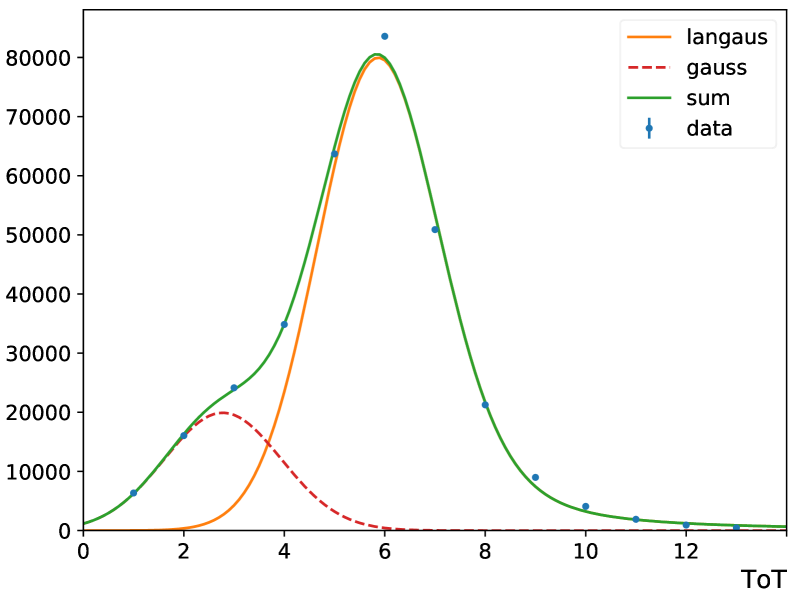
These measurements were performed at a bias voltage of 150 V. The ToT information, which corresponds to the collected charge, was obtained from this data and histogramed, sorted by cluster size. The resulting distribution for clusters of size 1 was fitted using a Landau-Gauss-convolution provided by pyLandau.444https://pypi.python.org/pypi/pyLandau To represent non-suppressed background from backscattered particles, a Gaussian is added. The fit for the unirradiated module is shown in Figure 7. The fit result for the MPV of the Landau-Gauss-convolution is ToT units.
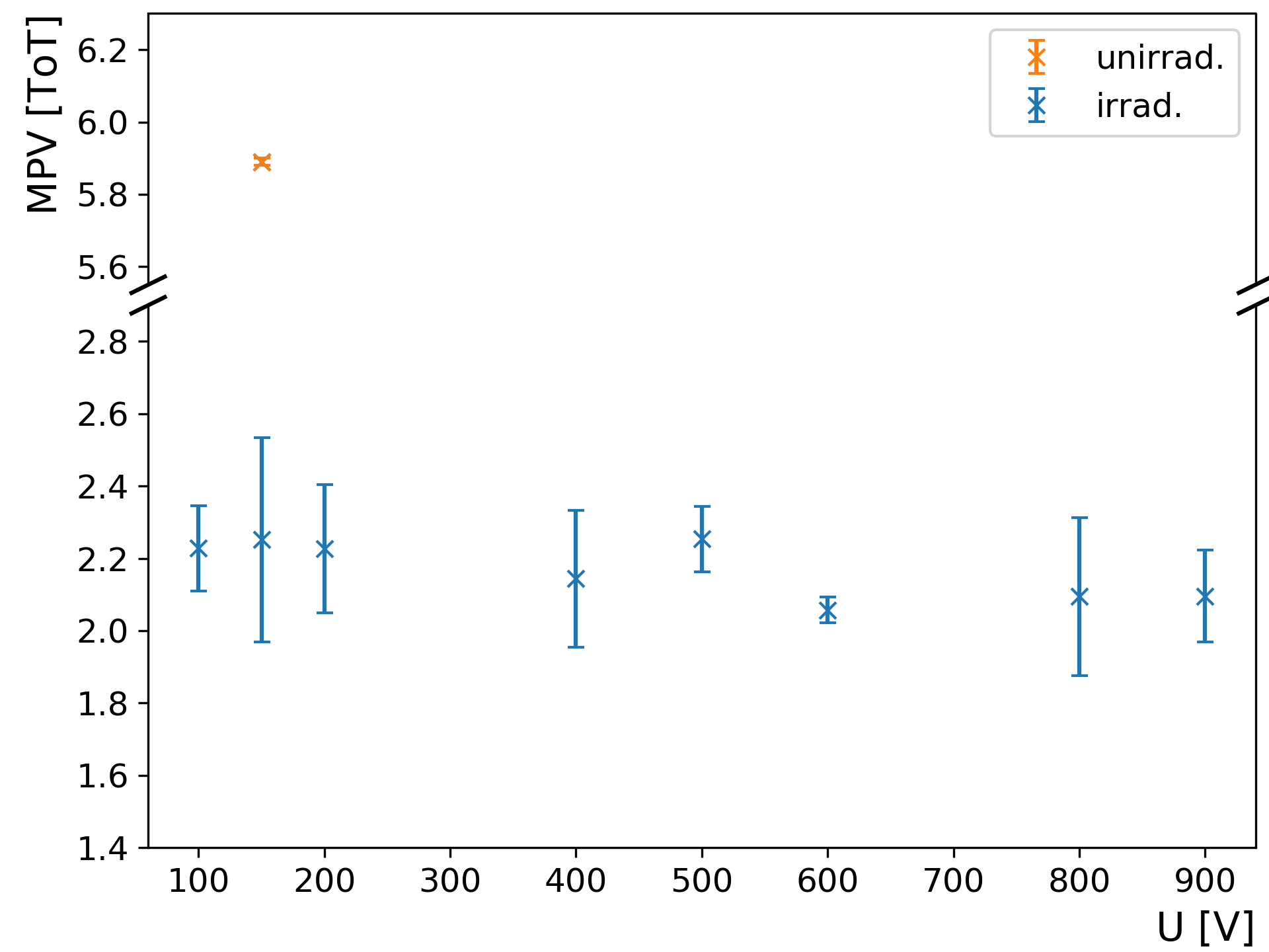
After irradiation, the module’s own radiation caused by activation was measured, using FE self-triggering, since the -source setup was not available. This method is more susceptible to noise. A bias scan was performed. The data was evaluated using the method described above. The result of MPV vs. bias voltage for the irradiated module is shown in Figure 7. The error bars result from the fit covariance matrix. The average MPV is 2.18 ToT units. As described in section 4, the same tuning was chosen for all measurements. This comparability allows to determine a reduction of the ToT signal to 40 % of the value before irradiation. This degradation can be improved easily by adjusting the tuning, leading to a larger ToT response at a similar charge in the sensor.
Due to the power dissipation of four FE chips, the external temperature sensors did not provide reliable values, but the sensor temperature was estimated to be -23 °C by comparing the leakage current during operation with the results obtained in section 3.
6 Testbeam measurements
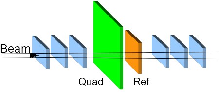
Before irradiation, measurements were performed with a pion beam of 120 GeV at CERN-SPS beamline H6. High tracking resolution is provided by six MIMOSA26 sensors of ACONITE, an EUDET-type telescope [11]. An unirradiated FE-I4 planar pixel module was used as the reference plane. A sketch of the setup is shown in Figure 8. A bias voltage of 150 V was applied to the quad sensor during all measurements. Unless stated otherwise, its front-end chips were tuned to a threshold of 3200 e and a response of 6 ToT at a reference charge of 20 ke.
Track reconstruction was performed with EUTelescope.555http://eutelescope.web.cern.ch/ For timing reasons, only tracks given by the telescope which match to hits in the reference plane are considered in the number of tracks . Each track which is also matched with a hit in the quad is considered in the number of hits . The pixel matching margin was set to 125 µm (50 µm) in X (Y), the cluster matching margin was set to 400 µm (250 µm) in X (Y). This analysis was performed with TBmon2.666https://bitbucket.org/TBmon2/tbmon2 The efficiency is defined as
| (6.1) |
its relative error is defined as
| (6.2) |
The recorded data were divided into runs with 16 k events each. The efficiency and its error was calculated for every run and every pixel geometry. A weighted mean was determined for all runs taken under the same condition. Figure 10 shows the combined efficiency map for three different measurement positions. No distinction can be observed between the ‘standard’, ‘long’, ‘ganged’ or ‘inter-ganged’ pixel designs. Figure 10 shows the in-pixel efficiency map of the ‘standard’ pixel design. The resulting efficiency is %. Figure 12 shows the in-pixel efficiency map of one ‘ganged’ pixel design. The resulting efficiency is %. It is overlayed with the layout of the two pixels with a distance of 300 µm, connected via a metal trace. The layout of the pixel in-between is not drawn. Comparable results with efficiencies well above 99.5 % were obtained for all other ‘ganged/inter-ganged pixels’ as well as ‘long pixels’.
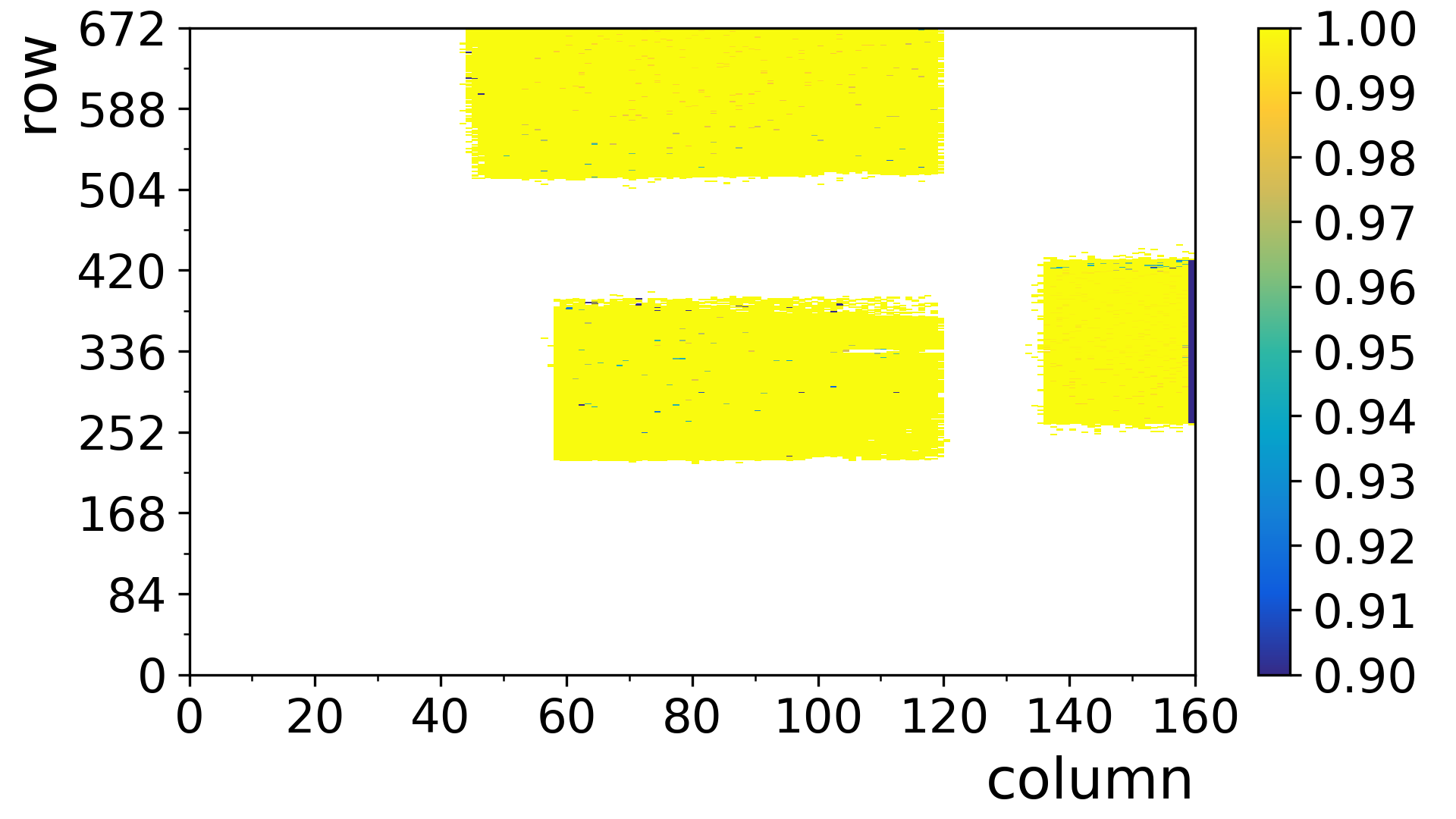
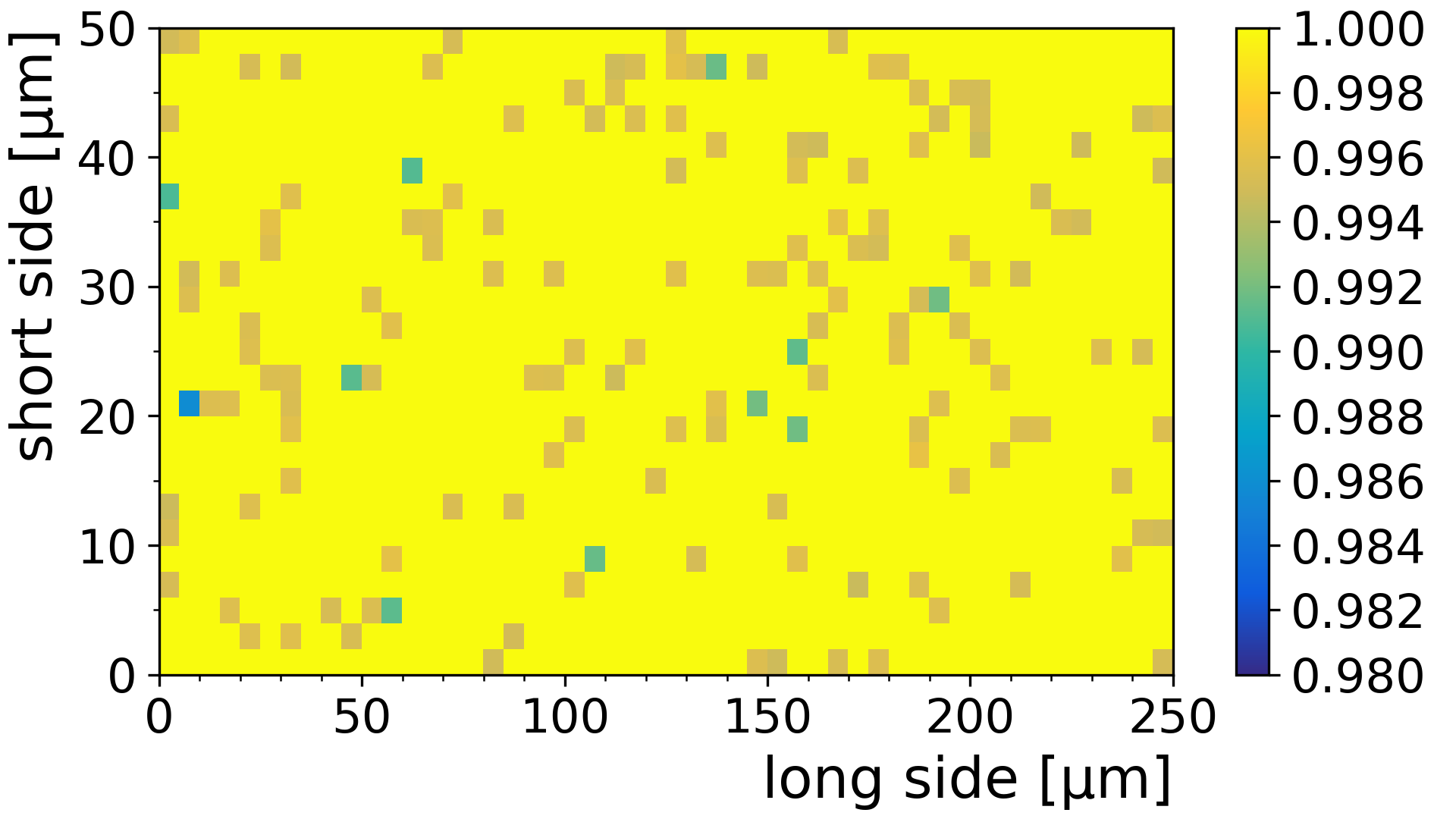
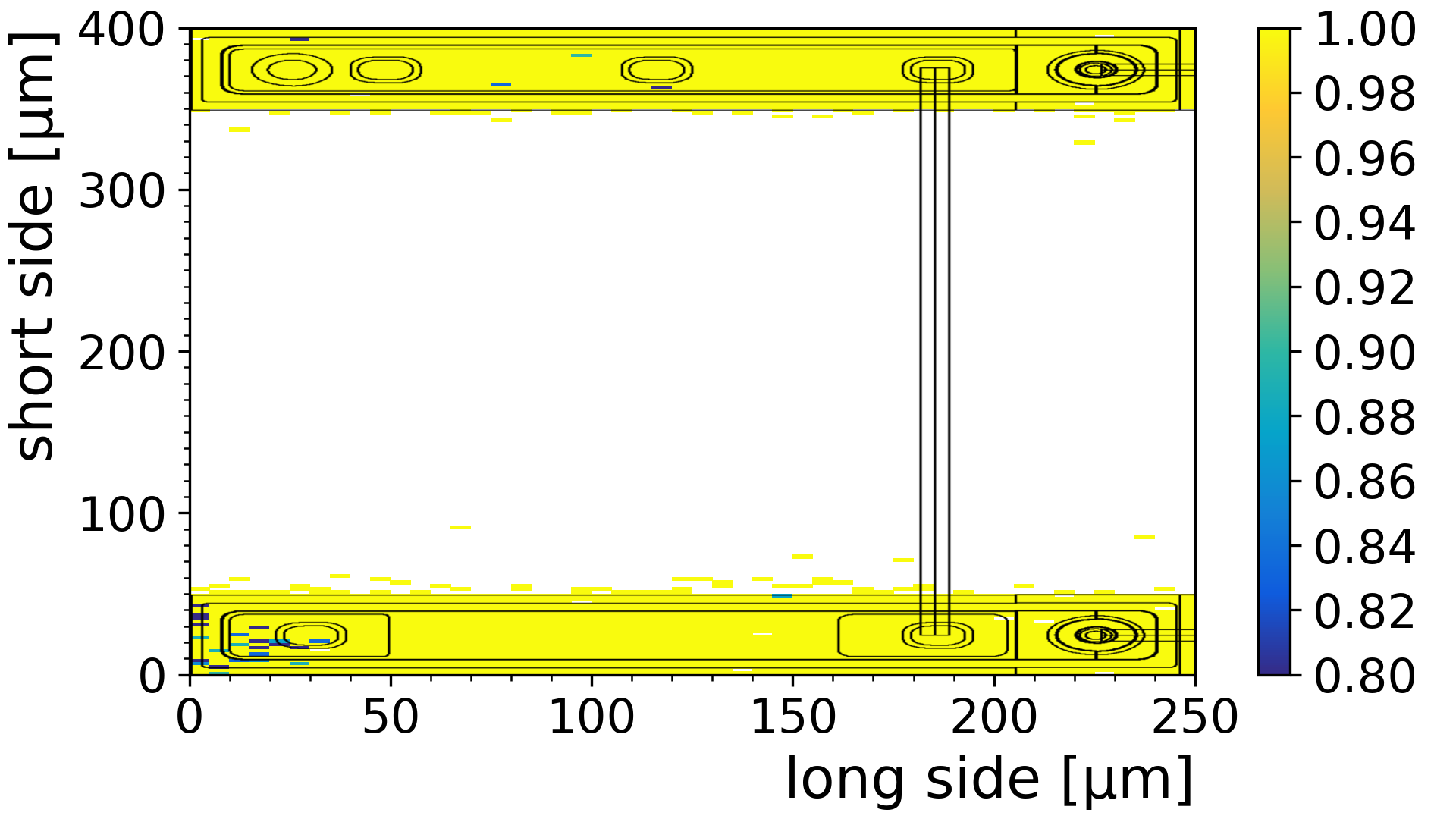
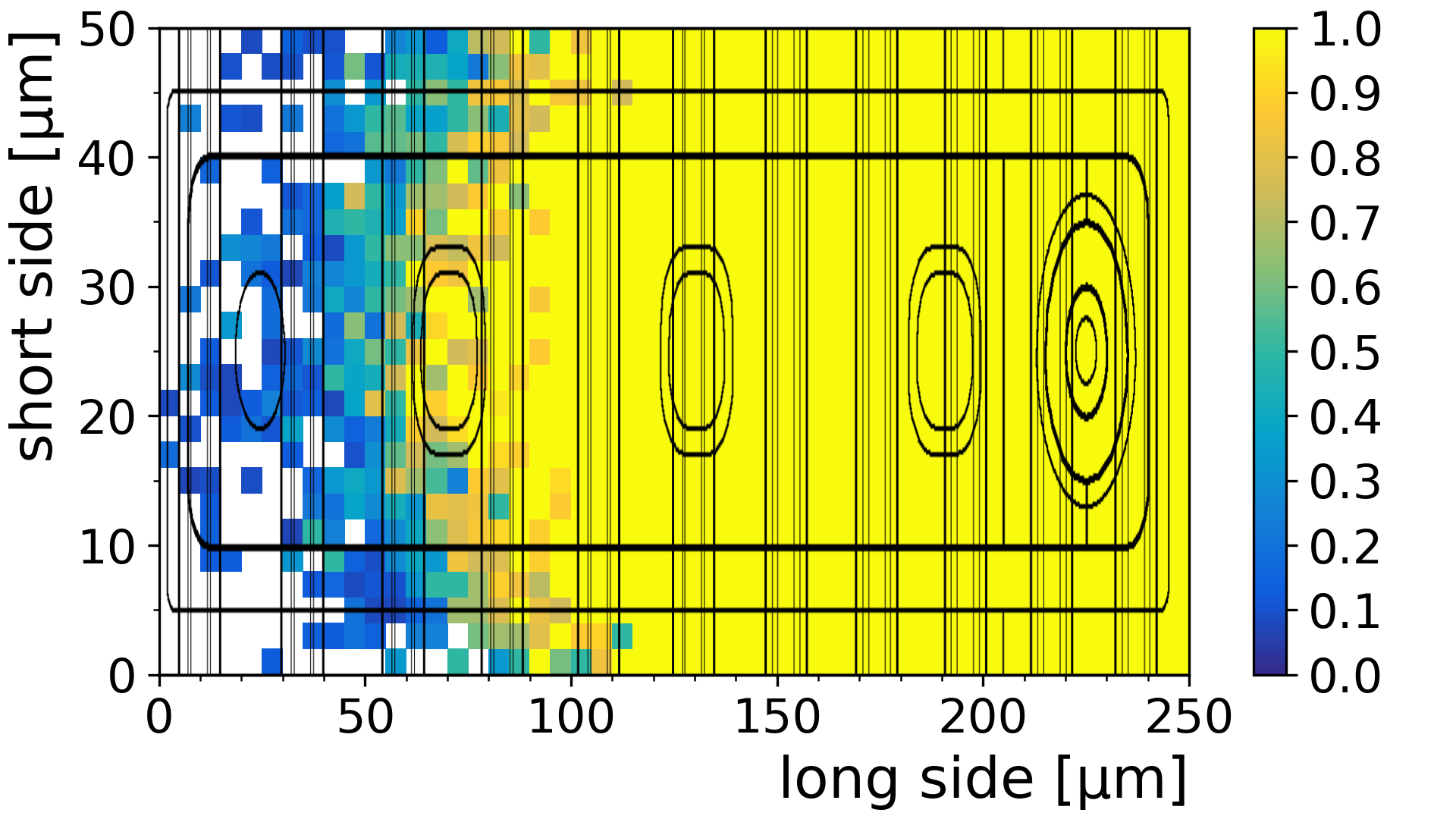
Figure 12 shows the in-pixel efficiency map of the ‘edge’ pixel design. The resulting efficiency is %, but it is revealed that the sensor is full efficient up to 150 µm beneath the guard rings. By lowering the threshold to 1600 e an improvement could be reached. The resulting efficiency of the ‘edge pixel’ for this threshold is %, the sensor is fully efficient up to 200 µm beneath the guard rings. This is consistent with results of IBL pre-studies [12], where 500 µm long pixels were partially shifted beneath the guard rings.
7 Summary
Fully working n-in-n quad modules were assembled. Promising results have been obtained for these modules in laboratory and testbeam measurements. MIP-like particles deposit a charge signal corresponding to 20 ke at a threshold of 3200 e. A tracking efficiency of more than 99.9 % has been measured for pixels with standard design which contribute to 95 % of all read-out channels. A successful analysis of pixel efficiency for ‘ganged’, ‘inter-ganged’ and ‘long’ designs was also performed, revealing a tracking efficiency well above 99.5 % for these special read-out channels.
After a first irradiation step, a slight degradation is visible as expected: The leakage current increases and the collected charge decreases, but no failures have been observed. Testbeam results after the next irradiation step are expected in October, followed by extensive lab investigations.
Acknowledgments
The possibility to irradiate detector samples at the CERN Proton Synchrotron Radiation Test Facility IRRAD [10] is kindly acknowledged, especially the help by F. Ravotti and G. Pezzullo.
Special thanks go to K. Wraight for the organization of this irradiation campaign, for the opportunity, and for the support to perform measurements with the irradiated quad module at the University of Glasgow.
The work presented here is carried out within the framework of Forschungsschwerpunkt FSP103 and supported by the Bundesministerium für Bildung und Forschung BMBF under Grants 05H15PECAA and 05H15PECA9.
References
- [1] G. Apollinari et al., High-Luminosity Large Hadron Collider (HL-LHC): Preliminary Design Report. CERN Yellow Reports: Monographs. CERN, 2015.
- [2] ATLAS Collaboration, The ATLAS Experiment at the CERN Large Hadron Collider, J. Instrum. 3 (2008) S08003.
- [3] ATLAS Collaboration, Letter of Intent for the Phase-II Upgrade of the ATLAS Experiment, Tech. Rep. CERN-LHCC-2012-022, CERN, 2012.
- [4] ATLAS Collaboration, ATLAS Phase-II Upgrade Scoping Document, Tech. Rep. CERN-LHCC-2015-020, CERN, 2015.
- [5] ATLAS Collaboration, Technical Design Report for the ATLAS Inner Tracker Strip Detector, Tech. Rep. CERN-LHCC-2017-005, CERN, 2017.
- [6] G. Aad et al., ATLAS pixel detector electronics and sensors, J. Instrum. 3 (2008) P07007.
- [7] M. Garcia-Sciveres et al., The FE-I4 pixel readout integrated circuit, Nucl. Instr. Meth. Phys. Res. A 636 (2011) S155 – S159.
- [8] ATLAS Collaboration, ATLAS Insertable B-Layer Technical Design Report, Tech. Rep. CERN-LHCC-2010-013, CERN, 2010.
- [9] ATLAS Collaboration, ATLAS Insertable B-Layer Technical Design Report Addendum, Tech. Rep. CERN-LHCC-2012-009, CERN, 2012.
- [10] F. Ravotti et al., A New High-Intensity Proton Irradiation Facility at the CERN PS East Area, PoS TIPP2014 (2014) 354.
- [11] H. Jansen et al., Performance of the EUDET-type beam telescopes, EPJ Tech. Instrum. 3 (2016) 7.
- [12] T. Wittig, Slim Edge Studies, Design and Quality Control of Planar ATLAS IBL Pixel Sensors. PhD thesis, TU Dortmund, 2013.