Van der Waals Schottky barriers as interface probes of the correlation between chemical potential shifts and charge density wave formation in 1T-TiSe2 and 2H-NbSe2
Abstract
Layered transition metal dichalcogenide (TMD) materials, i.e. 1T-TiSe2 and 2H-NbSe2, harbor a second order charge density wave (CDW) transition where phonons play a key role for the periodic modulations of conduction electron densities and associated lattice distortions. We systematically study the transport and capacitance characteristics over a wide temperature range of Schottky barriers formed by intimately contacting freshly exfoliated flakes of 1T-TiSe2 and 2H-NbSe2 to n-type GaAs semiconductor substrates. The extracted temperature-dependent parameters (zero-bias barrier height, ideality and built-in potential) reflect changes at the TMD/GaAs interface induced by CDW formation for both TMD materials. The measured built-in potential reveals chemical-potential shifts relating to CDW formation. With decreasing temperature a peak in the chemical-potential shifts during CDW evolution indicates a competition between electron energy re-distributions and a combination of lattice strain energies and Coulomb interactions. These modulations of chemical potential in CDW systems, such as 1T-TiSe2 and 2H-NbSe2 harboring second-order phase transitions, reflect a corresponding conversion from short to long-range order.
I Introduction
Understanding the mechanism of charge density wave (CDW) formation in low-dimensional correlated systems is of fundamental importance in condensed matter science, where studies of layered transition metal dichalcogenides (TMDs) harboring CDWs, such as 1T-TiSe2 and 2H-NbSe2tise1 ; tise2 ; nbse1 ; nbse2 , have revealed critical insights. The conventional weak-coupling mechanism driving the CDW state, known as the Peierls instability in 1-D, derives from Fermi surface nestingpeierls in which the energy gain associated with the formation of an energy gap separating filled and empty states is greater than the energy cost of forming a lattice distortion.gruner On the other hand CDW formation in 1T-TiSe2 and 2H-NbSe2 is believed to be a consequence of strong-couplingtise strong1 ; bond tise ; nbse2 ; nbse strong1 ; nbse strong2 ; nbse strong3 , where electron-electron or electron-phonon coupling is considered to be essential.
Direct observations by scanning tunneling spectroscopy/microscopy (STS/STM), angle-resolved photoemission spectroscopy (ARPES), X-ray powder diffraction (XRD), etc, have facilitated a better understanding of the physics of strong-coupling CDW systems. For example, in 2H-NbSe2 with a temperature-independent CDW wave vector, a short range CDW sets in at a temperature almost three times higher than the CDW transition temperature (33 K) where long range CDW order dominatesnbse1 . Accordingly, for 2H-NbSe2 the amplitude of the CDW order parameter is well defined within nanosized domains at higher temperaturenbse1 and the phase coherence gradually increases as the temperature is lowered towards an onset of long-range order with global phase coherence at nbse2 . The TMD, 1T-TiSe2, exhibits a different behavior. Here, although a short range coherent CDW state has been reported as welltise short1 ; tise short2 , the mechanism for CDW formation is associated with the opening of an indirect gap accompanied by the formation of excitonstise condensate . The amplitude of the order parameter is proportional to the gap and thus with decreasing temperature (for ) the amplitude increases towards saturation. For , 1T-TiSe2 is a semimetal and the CDW does not exist.
Transport measurements on CDW materials have traditionally provided evidence for a translational motion of the bulk CDW condensate in the presence of pinning to the underlying latticegruner . In this work we report systematic temperature-dependent current-voltage (-) and capacitance-voltage (-) measurements on Van der Waals junctions of 1T-TiSe2 and 2H-NbSe2 intimately contacted to moderately-doped n-type GaAs substrates. Specifically we find that mechanically exfoliated thin flakes of 1T-TiSe2 and 2H-NbSe2 form high quality Schottky barriers when placed into intimate contact with n-GaAs substrates with a nominal room-temperature doping concentration of 4.1 1016 cm-3. Advantageously our Schottky junctions serve as surface state probes that are sensitive to quasistatic chemical potential shifts that are associated with CDW formation in bulk.
II Sample fabrication and experimental methods
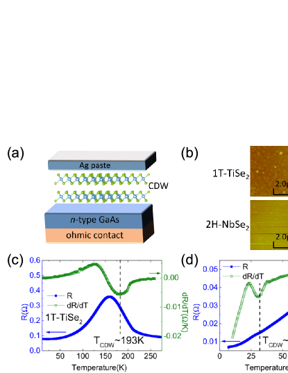
Mechanically exfoliated thin flakes of 1T-TiSe2 and 2H-NbSe2, with nominal thicknesses in the range 5-20 m, were transferred onto chemically cleaned n-type GaAs wafers as shown in Fig. 1(a). An RCA-I clean followed by a 3:1:50 HNO3:HF:H2O rinse for 2 minutes removed most native organics and oxides on the GaAs. According to our Hall measurements, the commercially available Si-doped GaAs(100) wafer had a nominal doping concentration of 4.1 1016 cm-3 at room temperature. Low resistance ohmic contacts to the GaAs wafers, robust to temperatures as low as 5 K, were made by rapid thermal annealing using a series of previously described recipesAng . As shown in Figs. 1(b) and (c), clean and flat flakes of cleaved 1T-TiSe2 and 2H-NbSe2, with root mean square surface roughness’s around 4Å from AFM images, guarantee intimate contact to the GaAs substrate. All measurements in the temperature range from 5 K to 300 K were carried out using a custom low-noise shielded chamber mounted in a Quantum Design Physical Properties Measurement System (PPMS). Four-terminal in-plane transport measurements for intrinsic crystals were performed using lock-in techniques at 526 Hz. DC - and AC - characteristics at kilohertz frequencies were acquired by a Keithley 2400 source meter and HP 4284A LCR meter. More than 10 devices for both 1T-TiSe2/n-GaAs and 2H-NbSe2/n-GaAs junctions were tested and shown to exhibit reproducible features. In Figs. 1 (c) and (d), we plot the in-plane resistance as well as the derivative with respect to temperature for thin flakes of 1T-TiSe2 and 2H-NbSe2 as a function of temperature, the CDW transition temperatures of 1T-TiSe2 and 2H-NbSe2 are respectively 193 K and 33 K.
III Schottky barriers as interface probes
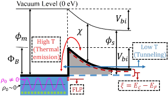
As shown in Fig.2, the measured built-in potential ideally is equal to the difference between the work functions of the TMD metallic electrode and of the adjacent semiconductorthermionic . In the presence of a correction for Fermi level pinning (FLP), the work function of the semiconductor is modified to be and becomes,
| (1) |
where the chemical potential is referred to the vacuum level where . There are two contributions to a temperature-dependent : the first derives from the semiconductor side where with denoting the intrinsic (donor dopant) density and the second derives from the TMD side where the chemical potential or work function shifts associated with CDW formation occur.
Accordingly, after normalizing out the well known changes arising from the temperature dependence of in GaAs, we are able - as shown in the paragraphs below - to utilize Eq. 1 to isolate and study the chemical potential shifts due to CDW formation in our 1T-TiSe2 electrodes. At low temperatures, 1T-TiSe2 is like a heavily doped semiconductor with a small gap and can be treated as a metallic electrode for this analysis. Similar signatures are also observed in 2H-NbSe2 based junctions indicating CDW-induced chemical potential shifts in 2H-NbSe2. For 2H-NbSe2, the observed evolves with decreasing temperature, suggesting a crossover from short range to long range CDW order below 90 K in accord with transport and STM measurementsnbse1 . Unexpectedly, for 1T-TiSe2, the short-to-long range CDW formation feature also appears when we closely analyze the temperature-dependent chemical potential shift in accord with Eq. 1. This common feature for two different materials with demonstrably different CDW formation mechanisms is somewhat surprising and presents a unifying theme embracing the nature of second-order CDW phase transitions in layered 2D TMD materials.
IV Results and discussions
According to transport measurement seen in Figs. 1(c) and (d), the CDW transition temperatures of 1T-TiSe2 and 2H-NbSe2 are respectively 193 K and 33 K, both of which are consistent with the literature on intrinsic bulk materialstise tCDW ; nbse tCDW . The - characteristics for 1T-TiSe2/n-GaAs and 2H-NbSe2/n-GaAs junctions are respectively shown in Figs. 3(a) and (b). The rectifying features indicate the formation of Schottky barriers when TMD-CDW materials are in intimate Van der Waals contact with GaAs substrates. The transport characteristics across Schottky barriers are well described by thermionic emission theory at high temperaturesthermionic where thermionic emission dominates. With phenomenological modificationsAng , the thermionic emission equation is also capable of describing the transport characteristics of Schottky barriers at low temperatures where field emission tunneling is also significant as illustrated in the schematic of Fig. 2.
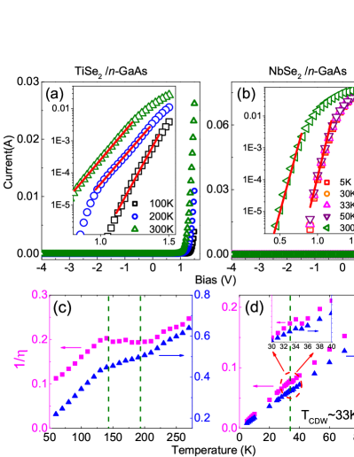
The temperature-dependent zero-bias barrier height and ideality factor characterizing the Schottky barrier profile can be extracted from the - characteristics, described by werner , where the contact resistance is negligible as it is for our junctions. These parameters and for both 1T-TiSe2/n-GaAs and 2H-NbSe2/n-GaAs junctions, are extracted by fitting from the linear regime of semi-log scaled - curves indicated in insets of Figs. 3 (a) and (b) and are shown in Figs. 3 (c) and (d) respectively.
The deflection or kink delineated by slope changes seen in Fig. 3(c) for the 1T-TiSe2/GaAs junction in the 140 K and 200 K range reveals CDW-induced changes in and corresponding to changes of the barrier profile. Such changes are the result of the transition from semimetal to semiconductor in 1T-TiSe2 related to the CDW formationtise2 . A similar, although less pronounced, kink signature is also apparent in the vicinity of 33 K for the 2H-NbSe2 as shown in Fig. 3(d), thereby corroborating the correlation between barrier profile change and CDW formation in 2H-NbSe2.
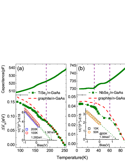
Complementary to forward-bias transport through the interface, capacitance measurements in reverse bias provide a direct measurement of and therefore a quasistatic method to characterize the depletion region and hence the Schottky barrier profile. Firstly, we notice the temperature-dependent zero-bias capacitance, as shown in the upper panels of Fig. 4(a) and (b), experiences a step-like anomaly spanning the range 150 K-200 K for 1T-TiSe2/n-GaAs and begins at 33 K-60 K for 2H-NbSe2/n-GaAs junctions with an upper bound determined below with further analysis. Here, at each temperature is extracted from extrapolated abscissa intercepts of linear versus reverse bias voltage plotsthermionic () shown for both 1T-TiSe2/n-GaAs and 2H-NbSe2/n-GaAs junctions at selected temperatures in the insets of Figs. 4(a) and (b).
Central to this paper is the understanding that measured built-in potentials for both metal/semiconductor (see Fig. 2) and heterojunctions reflect the difference between the work functions of the two materials in contactthermionic . For our doped GaAs substrates we calculate that deep within the GaAs the energy difference between the conduction band minimum and the chemical potential (Fermi energy) is small ( 60 mV at 300 K and near zero at low temperature) compared to , thereby justifying the use of the measured as a good estimate of the Schottky barrier height. The work functions of 1T-TiSe2 and 2H-NbSe2 at room temperature are around 5.4 eV and 5.6 eVsci adv , which for the 4.07 eV electron affinity of GaAs together with the Schottky-Mott law for ideal Schottky barriersmott gives Schottky barrier heights () of 1.33 eV and 1.53 eV for 1T-TiSe2/n-GaAs and 2H-NbSe2/n-GaAs junctions respectively. However, the barrier heights from our measurements at room temperature are somewhat lower at 1.1820.025 eV and 1.0540.010 eV respectively (the term is also included), indicating the presence of Fermi level pinning (FLP) effectstung .
To minimize these unavoidable FLP effects in our analysis, a certain temperature range with less FLP origins but overlapping the CDW transition regime is needed. The pinning coefficient is calculated by using the FLP relation with the charge neutrality level for simplicitytung , where is the barrier height from measurement, is the barrier height from the Schottky-Mott lawmott , and eV is the semiconductor band gap. As seen in the lower panels of Fig. 4, the temperature-dependent relative built-in potentials for both junctions are depicted as solid green squares. We note, as discussed earlier, that the background increase of with decreasing is due to the monotonic changes in in the semiconductor whereas the kink is due to CDW induced rearrangement of electron energy distributions in the TMD electrode. For the 1T-TiSe2/n-GaAs junction, we choose the reference temperature as 250 K, =1.2080.005 eV and , whereas K, =1.353 eV and for the 2H-NbSe2/n-GaAs junction. As a procedural check of these similarly calculated pinning coefficients, the results here for the tested devices are not sensitive to the the chosen reference temperatures within the vicinity of 20 K.
To further interpret our observed step-like anomalies in , we use graphite/n-GaAs junctions as reference junctions that are characterized by the same method as already discussed. The red dashed lines shown in Fig. 4 are data scaled by manually shifting the measured for the graphite/n-GaAs junction, with =1.082 eV and =1.252 eV, to the scale of 1T-TiSe2/n-GaAs and 2H-NbSe2/n-GaAs junctions respectively. Here, we consider highly ordered pyrolytic graphite (HOPG) to serve as the “ideal” Van der Waals featureless electrode for the following two reasons: Firstly, HOPG is also a 2D-layered material with a similar honeycomb crystal structure of TMD materials and secondly, HOPG exhibits no phase transition within the temperature range of 5 K to 300 K.
Since metal-induced gap states (MIGS) are strongly suppressed in Van der Waals junctionssci adv , we justifiably exclude the MIGS induced FLP effect at lower temperatures. In addition, since the lattice distortion’s amplitude during CDW formation in 1T-TiSe2 and 2H-NbSe2 is small compared to the in-plane distance between Se/Ti(Nb)–Se atomsbond tise ; bond nbse , we can also rule out the change of barrier height due to significant breaking of chemical bonds at the Schottky barrier interface. Moreover, with carrier density much higher than moderately doped semiconductors for both materialsnbse tCDW ; tise GL , we exclude the possibility of the observed changes originating from the modulation of interfacial dielectric properties during the CDW formation, a more pronounced mechanism that has already been reported in 1T-TaS2 harboring first-order CDW phase transitionsxc .
We consequently interpret the kink feature existing in both junctions as a chemical potential shift accompanying CDW formation in 1T-TiSe2 and 2H-NbSe2. Although the explicit correlation between CDW formation and chemical potential has already been discussed and confirmed in 1T-TiSe2 owing to the change of the associated order parameter’s amplitude during CDW formationtise condensate ; tise condensate theory , a corresponding shift in 2H-NbSe2 has to our knowledge not been reported.
In both 1T-TiSe2 and 2H-NbSe2, the CDW wave vector q is temperature independenttise tCDW ; nbse1 ; nbse2 . Therefore, only the CDW energy gap and the relative phase of the charge displacements characterize the CDW formation in both materialsgruner . From ARPES studies of 1T-TiSe2 at low temperaturestise condensate the change of the energy gap is associated with CDW formation raising the chemical potential by around 40 meV. However, a slight deviation of the experimental result from an exciton condensate model at temperatures ranging from 150 K to 200 K is noticedtise condensate ; tise condensate theory , which when combining with the signature of short range coherent CDWtise short1 ; tise short2 , indicates that changes in phase coherence are also significant for CDW formation in 1T-TiSe2. The case for CDW formation in 2H-NbSe2 is conversely, somewhat different. During the CDW formation in 2H-NbSe2, phase coherence is gradually developed and completed down to (from short range to long range CDW), whereas the amplitude of the CDW order parameter is well-defined with a finite amplitude over the temperature range starting from higher temperature as shown in a systematic work by Chatterjee et alnbse2 .
In this paper we are addressing evidence in support of the hypothesis that chemical potential shifts in a CDW material are linked with the evolution of a CDW’s complex order parameter comprising both amplitude and phase. To our knowledge there are no experiments that can simultaneously detect the amplitude and phase of the CDW order parameter. Our evidence (Fig. 5) for effective chemical potential shifts is derived from the differences between the scaled for graphite/n-GaAs junction (red) and for both junctions (green) shown in Fig. 4, . Inclusion of FLP effects does not change the monotonic relation between the change of Fermi level and barrier height. Accordingly, FLP effects clearly exist but do not modify our conclusions.
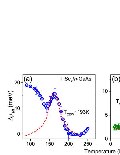
To gain a physical understanding of the peak features shown in Fig. 5, we re-emphasize that CDW formation primarily affects and not of Eq. 1. Hence, with decreasing temperature for both TMD materials, the high(low) temperature side of the respective peaks (red dashed lines) represents a simultaneous increase(decrease) in the quantities , and . The changes in only manifest the changes in electronic energy associated with the redistribution of electrons in the Fermi sea and are not directly sensitive to Coulomb and strain energies. Accordingly, total energies are not measured. However, in the region of the peaks there is a delicate balance over a narrow temperature range where, on the low(high) temperature side of the peak, electronic energies are(are not) favored. For 1T-TiSe2 photoemission measurementstise condensate show a gradually increasing chemical potential upon cooling, in agreement with the overall trend in Fig. 5(a) but without sufficient resolution to show the peak near 170 K. This increase in chemical potential is interpreted in Ref. tise condensate as a temperature-dependent during CDW formation mediated by excitons. A similar hump-like feature, peaked at around 50 K, is more pronounced in 2H-NbSe2 as seen in Fig.5(b) signifying common aspects of CDW formation in both 1T-TiSe2 and 2H-NbSe2. In both systems the phase coherence increases with decreasing temperature where homogeneous CDW domains with constant phase at low temperatures have evolved from locally isolated CDW domains dominating at higher temperaturesnbse1 .
V Conclusions
In summary, by use of “simple” Van der Waals Schottky barriers between layered TMD materials and the moderately doped semiconductor n-type GaAs, we have found common features of CDW formation in 1T-TiSe2 and 2H-NbSe2. These common features suggest that similar considerations may apply to other layered TMD strong-coupling CDW materials. Our insights provide a complementary understanding of the mechanism of CDW formation in low-dimensional correlated systems and have shown a promising route for detecting and analyzing collective interfacial phenomena arising from strong correlation. The use of Schottky barriers as surface state probes not only enlightens our understanding of the electronic states in low dimensional correlated systems but also suggests technological applications.
VI Acknowledgements
The authors thank Andrew Rinzler for useful discussions and the Nanoscale Research Facility at the University of Florida for access to cleanroom and rapid thermal annealing facilities. †A. J. Li and X. Zhu contributed equally to this work. This research work was supported by the National Science Foundation under Grant No. DMR–1305783 (AFH), the U.S. Army Research Office through the MURI Grant No. W911NF-11-10362 (LB) and the ONR-DURIP Grant No. 11997003 (LB).
References
- (1) L. J. Li, E. C. T. O’Farrell, K. P. Loh, G. Eda, B. Ozyilmaz, and A. H. Castro Neto, Nature 529, 185 (2016).
- (2) M. Porer, U. Leierseder, J.-M. Menard, H. Dachraoui, L. Mouchliadis, I. E. Perakis, U. Heinzmann, J. Demsar, K. Rossnagel, and R. Huber, Nat. Mater. 13, 857 (2014).
- (3) C. J. Arguello, S. P. Chockalingam, E. P. Rosenthal, L. Zhao, C. Gutiérrez, J. H. Kang, W. C. Chung, R. M. Fernandes, S. Jia, A. J. Millis, R. J. Cava, and A. N. Pasupathy, Phys. Rev. B 89, 235115 (2014).
- (4) U. Chatterjee, J. Zhao, M. Iavarone, R. Di Capua, J. P. Castellan, G. Karapetrov, C. D. Malliakas, M. G. Kanatzidis, H. Claus, J. P. C. Ruff, F. Weber, J. van Wezel, J. C. Campuzano, R. Osborn, M. Randeria, N. Trivedi, M. R. Norman, and S. Rosenkranz, Nat. Commun. 6, 6313 (2015).
- (5) R. Peierls, More Surprises in Theoretical Physics (Princeton University Press, Princeton, NJ, 1991).
- (6) G. Grüner, Rev. Mod. Phys. 60, 1129 (1988).
- (7) K. Rossnagel, J. Phys.: Condens. Matter 23, 213001 (2011).
- (8) F. Weber, S. Rosenkranz, J.-P. Castellan, R. Osborn, G. Karapetrov, R. Hott, R. Heid, K.-P. Bohnen, and A. Alatas, Phys. Rev. Lett. 107, 266401 (2011).
- (9) T. Valla, A. V. Fedorov, P. D. Johnson, P. A. Glans, C. McGuinness, K. E. Smith, E. Y. Andrei, and H. Berger, Phys. Rev. Lett. 92, 086401 (2004).
- (10) F. Weber, S. Rosenkranz, J.-P. Castellan, R. Osborn, R. Hott, R, R. Heid, K-P. Bohnen, T. Egami, A. H. Said, and D. Reznik, Phys. Rev. Lett. 107, 107403 (2011).
- (11) C. J. Arguello, E. P. Rosenthal, E. F. Andrade, W. Jin, P. C. Yeh, N. Zaki, S. Jia, R. J. Cava, R. M. Fernandes, A. J. Millis, T. Valla, R. M. Osgood, Jr., and A. N. Pasupathy, Phys. Rev. Lett. 114, 037001 (2015).
- (12) C. S. Snow, J. F. Karpus, S. L. Cooper, T. E. Kidd, and T.-C. Chiang, Phys. Rev. Lett. 91, 136402 (2003).
- (13) B. Hildebrand, T. Jaouen, C. Didiot, E. Razzoli, G. Monney, M.-L. Mottas, A. Ubaldini, H. Berger, C. Barreteau, H. Beck, D. R. Bowler, and P. Aebi. Phys. Rev. B 93, 125140 (2016).
- (14) C. Monney, E. F. Schwier, M. G. Garnier, N. Mariotti, C. Didiot, H. Beck, P. Aebi, H. Cercellier, J. Marcus, C. Battaglia, H. Berger, and A. N. Titov, Phys. Rev. B 81, 155104 (2010).
- (15) A. J. Li and A. F. Hebard, J. Phys. D: Appl. Phys. 49, 455101 (2016).
- (16) S. M. Sze, and K. K. Ng, 2006 Physics of Semiconductor Devices (New York: Wiley).
- (17) F. J. Di Salvo, D. E. Moncton, and J. V. Waszczak, Phys. Rev. B 14, 4321 (1976).
- (18) H. N. S. Lee, M. Garcia, H. McKinzie, and A. Wold, J. Solid State Chem. 1, 190–194 (1970). J. Edwards and R. F. Frindt, J. Phys. Chem. Solids 32, 2217 (1971).
- (19) H. H. Güttler, and J. H. Werner, Appl. Phys. Lett. 56, 1113 (1990).
- (20) Y. Liu, P. Stradins, and S. Wei, Sci. Adv. 2, e1600069 (2016).
- (21) N. F. Mott, Proc. R. Soc. Lond. A 171, 27 (1939).
- (22) R. Tung, Mater. Sci. Eng., R. 35, 1 (2001).
- (23) C. D. Malliakas, and M. G. Kanatzidis, J. Am. Chem. Soc. 135, 1719 (2013).
- (24) G. Li, W. Z. Hu, D. Qian, D. Hsieh, M. Z. Hasan, E. Morosan, R. J. Cava, and N. L. Wang, Phys. Rev. Lett. 99, 027404 (2007).
- (25) X. Zhu, A. J. Li, G. R. Stewart, and A. F. Hebard, Appl. Phys. Lett. 110, 181603 (2017).
- (26) C. Monney, H. Cercellier, C. Battaglia, E. F. Schwier, C. Didiot, M. G. Garnier, H. Beck, and P. Aebi, Physica B 404, 3172 (2009).