Magnetic-field driven ambipolar quantum Hall effect in epitaxial graphene close to the charge neutrality point
Abstract
We have investigated the disorder of epitaxial graphene close to the charge neutrality point (CNP) by various methods: i) at room temperature, by analyzing the dependence of the resistivity on the Hall coefficient ; ii) by fitting the temperature dependence of the Hall coefficient down to liquid helium temperature; iii) by fitting the magnetoresistances at low temperature. All methods converge to give a disorder amplitude of meV. Because of this relatively low disorder, close to the CNP, at low temperature, the sample resistivity does not exhibit the standard value but diverges. Moreover, the magnetoresistance curves have a unique ambipolar behavior, which has been systematically observed for all studied samples. This is a signature of both asymmetry in the density of states and in-plane charge transfer. The microscopic origin of this behavior cannot be unambiguously determined. However, we propose a model in which the SiC substrate steps qualitatively explain the ambipolar behavior.
I Introduction
Undoubtedly, the best known exotic two-dimensional electron system is graphene.Geim and Novoselov (2007) Among various exciting properties, this material has demonstrated a half-integer quantum Hall effect Zhang et al. (2005) (QHE) which is very robust in temperature,Novoselov et al. (2007) because of the extremely large energy separation between the first Landau levels (LL) lying close to the bottom of conduction and valence bands.
The QHE in graphene is strongly influenced by disorder and hence by the choice of the substrate. The quantum Hall plateaus observed in graphene on SiC (G/SiC) have a high breakdown currentAlexander-Webber et al. (2013) and appear at lower magnetic fieldsHuang et al. (2015) with respect to graphene deposited on SiO2.Poumirol et al. (2010) The quantum plateaus in G/SiC devices are much larger in magnetic field than those obtained in graphene encapsulated in hBN,Dean et al. (2011) because they are stabilized by charge transferJanssen et al. (2011) and disorder.Lafont et al. (2015)Thanks to these properties, it was recently demonstrated that G/SiC can act as a quantum electrical resistance standard,Tzalenchuk et al. (2010) even in experimental conditions relaxed with respect to the state-of-the-art in GaAs-based quantum wells.Ribeiro-Palau et al. (2015)
To date, fundamental and practical questions remain open. In particular, the fate of the G/SiC quantum plateaus close to the charge neutrality point (CNP) has still to be elucidated. Achieving and controlling low doping is of primary interest to use graphene as a resistance standard at even lower magnetic fields, or in cryogen-free systems.Janssen et al. (2015) G/SiC could be also a material of choice for testing theoretical models predicting additional quantum plateaus depending on the type of disorder.Nomura et al. (2008); Ostrovsky et al. (2008)
However, there exist only a few experimental analyses of the transport properties close to the CNP,Huang et al. (2015) mainly because G/SiC is intrinsically strongly -doped by the SiC substrate, thus requiring the system to be compensated by a top gate. For graphene on SiO2, close to the CNP, QHE reveals that electrons and holes coexist even when the energy spectrum is quantized and the carriers partially localized,Wiedmann et al. (2011); Kurganova et al. (2013) but for G/SiC even this rather intuitive picture has not been thoroughly tested. The amplitude of the disorder potential fluctuation has been evaluated by various methods,Curtin et al. (2011); Huang et al. (2015) but the type of disorder and its spatial and energy distribution close to CNP remain mostly unknown.
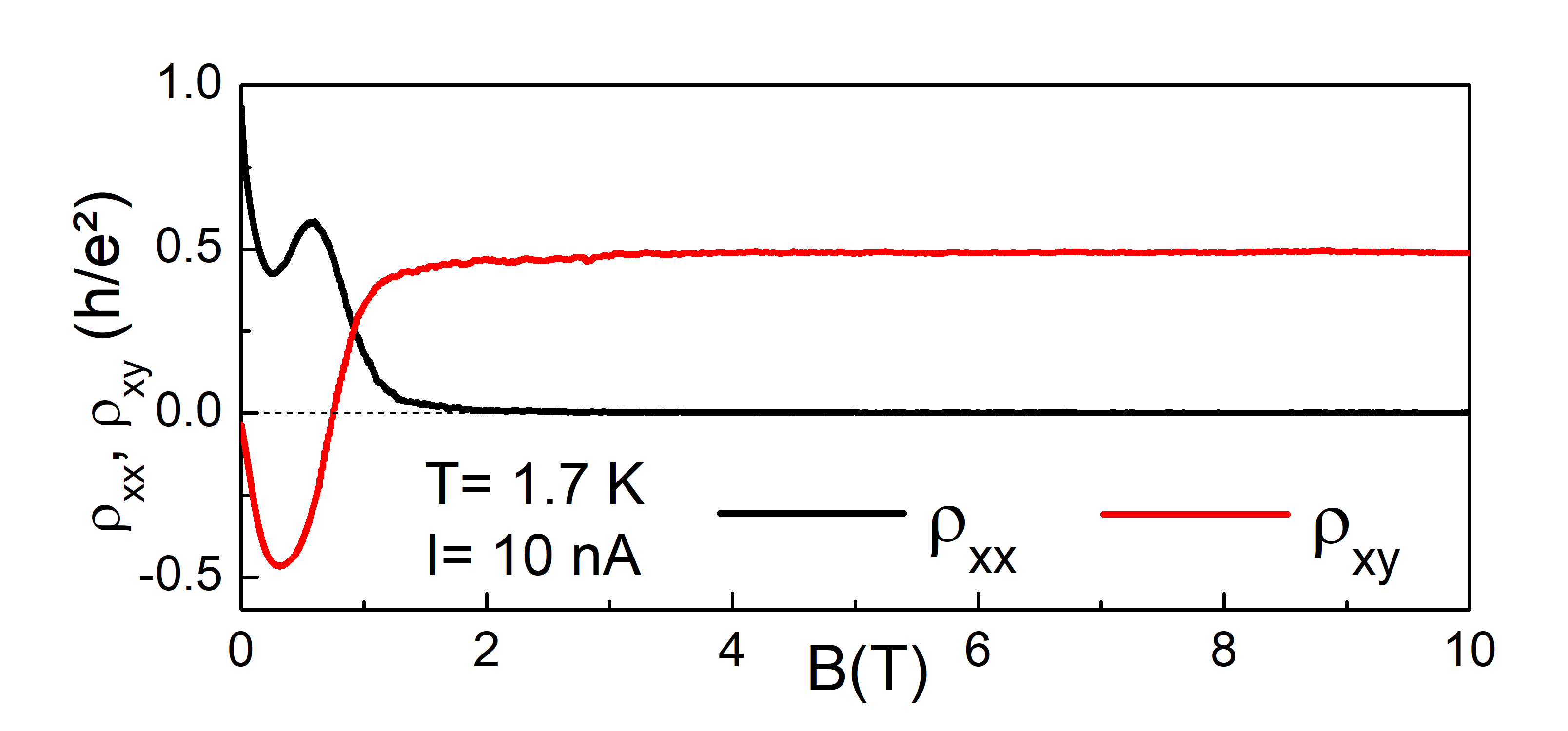
In this paper, we present magnetotransport experiments in G/SiC to evaluate the disorder and to test the stability of the QHE close the CNP. The results are largely unexpected and reveal new physics in comparison to what is observed on other substrates. We show that not only electrons and holes coexist in high magnetic fields, but the carriers also redistribute unexpectedly as a function of magnetic field , as illustrated in Fig. 1. In this figure, the graphene is tuned very close to the CNP. The magnetoresistance reveals a magnetic field driven ambipolar QHE. At low , a quantized -like plateau starts to develop. However, when is increased further, this plateau collapses and is replaced by a quantized -like plateau of opposite sign. We show that this behavior is robust and reproducible for the range of doping where both types of carriers coexist and we propose a model based on disorder and in-plane charge transfer, after a detailed analysis of the sample disorder close to the CNP.
II Methods and methodology
II.1 Sample fabrication
The SiC/G samples have been grown epitaxially on the Si-face of a semi-insulating 4H-SiC substrate at a high temperature °C. The as-grown samples have large uniform monolayer areas. Atomic force microscope analysis revealed the presence of SiC steps, approximately 500 nm wide and 2 nm high, uniformly covered by the graphene layer. Additional Raman analysis revealed the presence of elongated bilayer graphene patches, approximately 10 µm long and 2 µm wide, covering around 5% of the total surface.
Hall bars of various size and geometry were then fabricated by standard electron-beam lithography. The graphene was covered by two layers of resist, as described in Ref. Lara-Avila et al., 2011. The resist acts as a chemical gate and strongly reduces the intrinsic carrier density of the graphene layer.
Magnetotransport measurements were performed on four SiC/G Hall bars, named G14, G31, G21 and G34. The bars have a length of 420 µm and a width of 100 µm, except for G34, which has a width of 20 µm.
II.2 Corona preparation
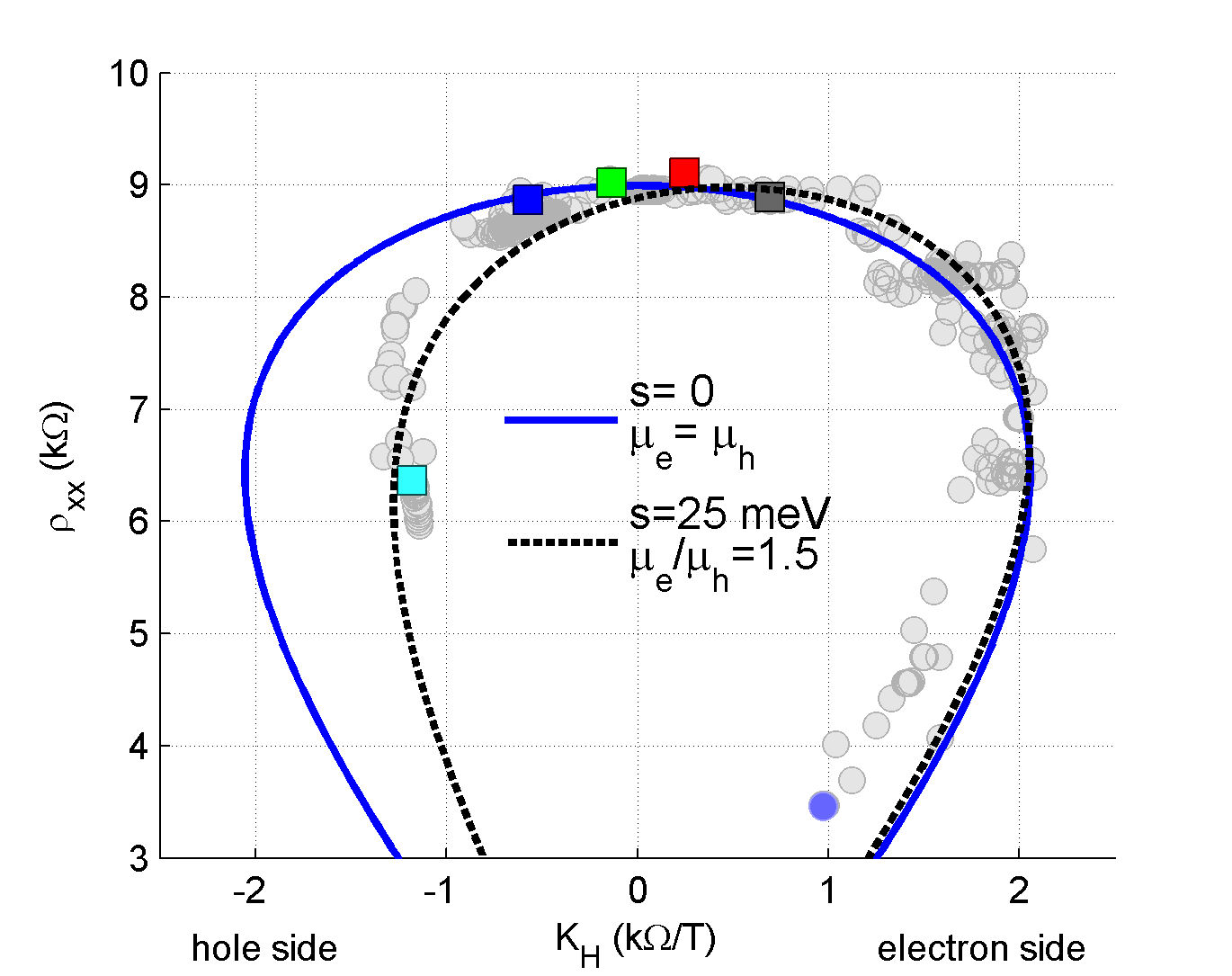
After the lithography process, the graphene layer was systematically -doped with cm-2 at room temperature. Carrier density control was performed with ion projections onto the resist bilayer covering graphene. Negative ions were produced by repeated corona discharges with a time interval of 17 s, following the method described in Ref. Lartsev et al., 2014. The distance between the sample and the corona source was 12 mm. Changes in the electronic properties of graphene upon exposure to corona ions were detected by continuous measurements of the resistance and Hall coefficient at room temperature, using low magnetic field (= 0.05 T) and dc current µA. The evolution of the resistivity as a function of the Hall coefficient during exposure to ions is presented in Fig. 2. There is some point dispersion due to the absence of correlation between the discharges and the electrical measurements. However, the carrier density clearly changes from its initial -doping of cm-2 to a -doping of cm-2 after a few hundreds cycles of corona discharge. After this point, additional ion projections are inefficient to increase further the -doping. When the discharges are stopped, the carrier density drifts slowly towards -doping and stabilizes around k/T within a few hours. The initial carrier density is not recovered even when the sample is left several months under ambient atmosphere.
III Estimation of disorder
III.1 Disorder estimated from at room temperature
To describe the sample evolution seen in Fig. 2, we use the usual equations Li et al. (2011) that give the conduction of a homogeneous sample, in which both electrons and holes participate in the conduction in parallel because of thermal activation. The model is detailed in Annex. The modeled ) curve is plotted for cm2/Vs and K as a blue solid line in Fig. 2a when spans the energy window around the CNP. Here, , and are the electron mobility, hole mobility and chemical potential respectively. The model fits fairly well the data but with an obvious deviation on the hole side, where the coefficient is overestimated. The asymmetry of the ) curve indicates that and differ. The data can be modeled more precisely in two ways: i) the mobility ratio increases when the number of deposited ions increases because negative ions have a larger cross section for -type charge carriers and their presence can decrease significantly the hole mobility Novikov (2007); ii) and does not depend on the charge carrier concentration but disorder has to be taken into account.
III.2 Disorder estimated from
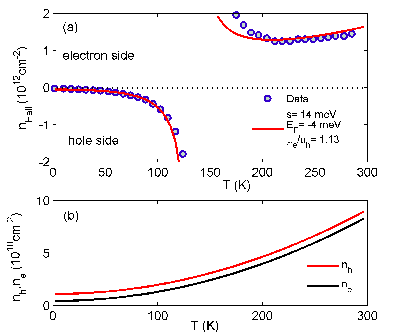
The disorder can also be estimated from the temperature dependence of the Hall coefficient. Fig. 3a shows the evolution of the Hall density of sample G14 when is lowered from room temperature down to 1.7 K. The initial corona preparation has been chosen to illustrate that one should not expect a dependence of the Hall density as a universal trend, as assumed in Ref. Huang et al., 2015. In Fig. 3a, the Hall density diverges at a critical temperature K, is negative below and positive above . This divergence is a clear signature that both electrons and holes participate in the conduction and from Eq. 5, can be identified as the temperature for which . We stress that this change of sign of does not imply that the net carrier density changes with . Let us assume, as in Refs. Li et al., 2011 and Huang et al., 2015, that the net carrier density does not depend on . It is possible to fit the data taking into account 3 parameters: the disorder amplitude , the Fermi energy at zero temperature , and the mobility ratio . From the fit of the temperature dependence shown in Fig. 3a, we extract meV, = -4 meV and . The fit matches very well the data, except in the vicinity of , where the experimental error is larger as the measured voltage cancels. Fig. 3b shows that and increase quadratically with .
From various fits corresponding to 11 different initial corona preparations, we found meV and . These parameters are roughly in agreement with those extracted from the fit. However, the precision is not good enough to evidence a possible evolution of with the progressive ion deposition.
IV Ambipolar quantum Hall effect
IV.1 Experimental results
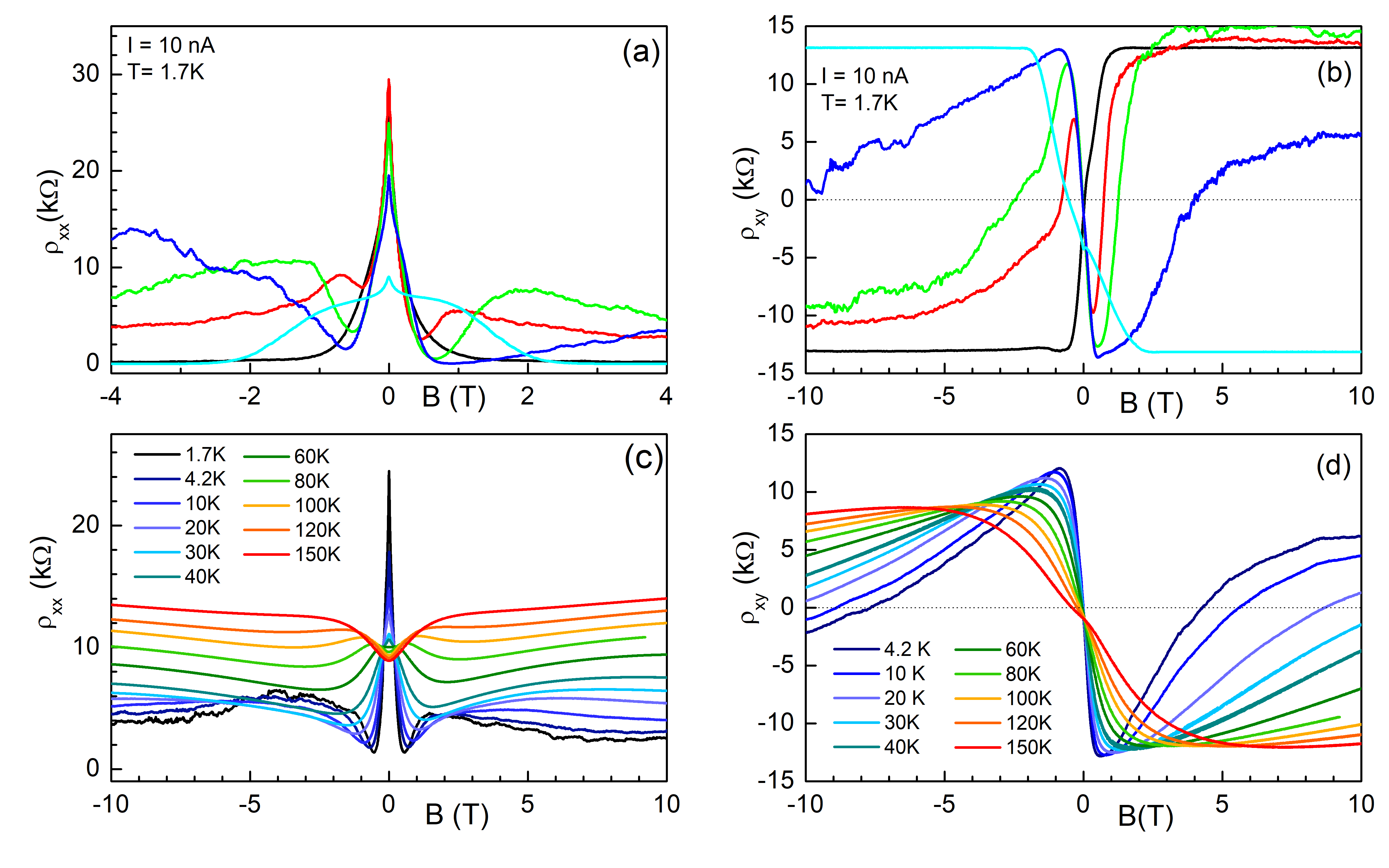
Fig. 4a,b shows the longitudinal and transverse magnetoresistances at K for sample G14. Five different dopings, indicated in Fig. 2 by colored squares, were first obtained at room temperature by the corona method. For each of these initial preparations, the sample was introduced in the cryostat and cooled down.
We first note that the longitudinal resistance is unusual. There is a pronounced negative magnetoresistance peak around T, see Fig. 4a. The peak value is close to at = 1.7 K, and largely exceeds the pseudo-universalAdam et al. (2007) value of usually observed in graphene on SiO2 close to the CNP. We checked that increases even further, up to k, when the temperature is decreased down to 280 mK. This insulating behavior, see Fig. 4c, shares strong similarities with a previous experiment,Ponomarenko et al. (2011) where an insulating behavior observed in graphene encapsulated in hBN was attributed to Anderson localization. Following Ref. Ponomarenko et al., 2011, such a localization can only be observed if the carrier density in the puddles is small enough (around cm-2 in Ref. Ponomarenko et al., 2011), in good agreement with our own estimation of the disorder in G/SiC ( meV yields cm-2.)
We now focus on the Hall magnetoresistance. First, the usual half-integer QHE is observed for high -doping ( cm-2, panel b, cyan curve) or low -doping ( cm-2, panel b, black curve). Between these two dopings, the plateaus are not well defined. However, the Hall magnetoresistance systematically follows a remarkable behavior. Increasing , there is first a decrease of , followed by a saturation at or before (-like plateau), where . Then, collapses, changes its sign and finally stabilizes at a positive value close to (-like plateau). Using pulsed magnetic fields, we checked that there is no more change of sign of at least up to 30 T. We never observed the opposite transition, from -like to -like plateau.
In some other measurements, as shown in Fig. 1, a well defined plateau has been observed at . The magnetic field at which cancels is also related with the appearance of a bump on , see Fig. 1 and Fig. 4a. The position of this bump seems to be also related with the initial doping obtained at room temperature. When graphene is slightly -doped at room temperature, this bump appears at low (red curve in panel a). When graphene becomes progressively more -doped, the bump shifts to higher (green and blue curves in panel a) and finally disappears (cyan curve).
Finally both and show a clear temperature dependence, as shown in panels c,d. The additional bump goes to higher when increases and then disappears. The behavior is even more striking, as the ambipolar behavior disappears above K and is replaced by an almost quantized plateau corresponding to an apparent -doping.
IV.2 Inadequacy of the standard two fluid model
The two fluid Drude model (Eqs. 5 and 6) can explain in some cases a change of sign of . This is because at low , whereas at high , . However, Fig. 4d shows that in the high field limit T, is positive at low . This is in contradiction with the previous temperature analysis, which indicates that at all . Moreover is negative at low , which, in the framework of two fluid Drude model, indicates that holes are more mobile than electrons, in contradiction with all our previous analyses. Additionally, the Drude model is not valid in the quantum Hall regime studied here and predicts only monotonous positive longitudinal magnetoresistance, in contradiction with the observation of a bump in at finite . Obviously, the two fluid model fails to explain the magnetoresistances and another explanation is needed to account for all of these observations.
IV.3 Disorder-induced charge transfer model
A rather similar ambipolar behavior was reported in graphene on SiO2 substrate and interpreted as being due to important disorder.Poumirol et al. (2010) Here, changes sign at much smaller and the QHE is rather well preserved, suggesting that the disorder amplitude is much smaller.
Besides, charge transfer has already been identified as being a major source of charge redistribution in G/SiC when the magnetic field evolves.Janssen et al. (2011) The SiC interface states and graphene are coupled by a quantum capacitance, which depends on the graphene density of states (DOS) and hence on .Kopylov et al. (2010) Additional in-plane charge transfers, induced by disorder, have also been identified in G/SiC when the overall top gate is degraded.Yang et al. (2016) Here, the photochemical top gates have kept their integrity (as routinely observed optically). Nevertheless, we show in the following that in-plane charge transfer explain the observed ambipolar QHE.
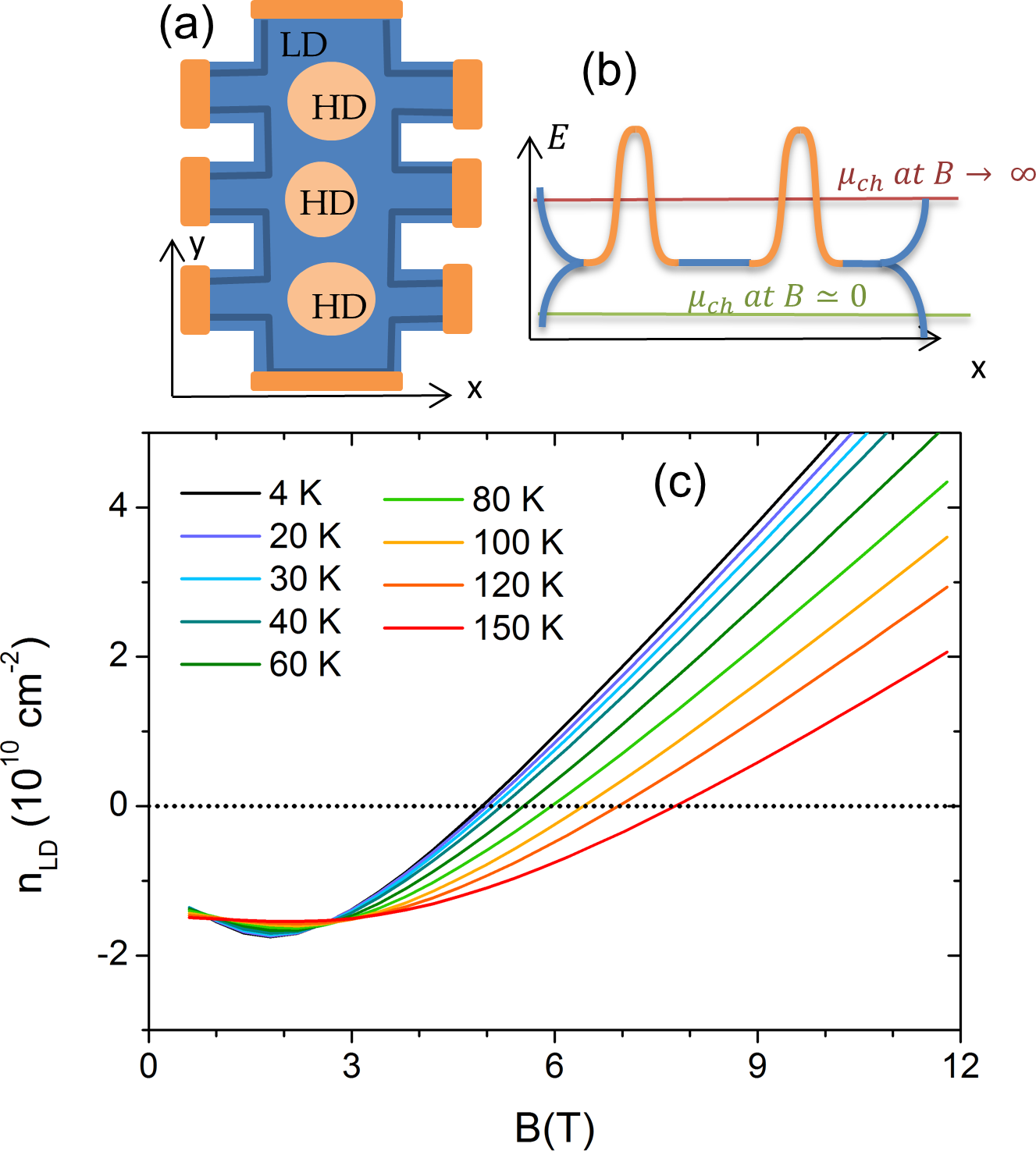
Let us assume that the main part of the Hall bar is homogeneous, with a low and uniform -doping. This region is referred to as the low doped (LD) region. However, the device also contains a few highly doped (HD) regions where the -doping is higher (Fig. 5a). The key ingredient of the model is that, in the quantum regime, the conductivity is governed by the edge states of the LD region. The HD regions do not percolate, do not participate in the conduction and only act as additional charge reservoirs.
The possible microscopic origins of these regions are multiple. For instance, the role of ionized acceptors in a quantizing magnetic field is well documented in the literature.Kubisa and Zawadzki (1996) They trap electrons, create an impurity band in the DOS of the LLs at high energies and shift the position of the quantum plateaus in two-dimensional electron gases.Haug et al. (1987) In our case, the ions trapped in the resist could act as magneto-acceptors, but we have no definitive proof for this scenario.
In what follows, we propose another microscopic origin for the HD regions. It is well known that the SiC surface is not flat but has a step-like structure. The graphene layer is lifted from the SiC surface close to the SiC step edges. There, the quantum capacitance between graphene and the SiC interface is reduced, leading to a larger -doping.Low et al. (2012)
At low magnetic field, graphene can be prepared in such a way that is below the delocalized states of the LD region and the conductivity is governed by edge states which have a hole character, as illustrated in Fig. 5b (green line). When the magnetic field is increased, the LL degeneracy increases. As the total net carrier density (including LD and HD regions) tends to remain constant, moves to higher energy (red line). When the magnetic field is high enough, has shifted between the LL energies of the LD and HD regions. There, the LD region has become -doped whereas the HD puddles are still -doped. The conductivity is then governed by the LD edge states which have now an electron character. Experimentally, the magnetic field at which reverses can be as low as T, which gives the minimal size of the HD regions: 40 nm.
Below we derive numerical estimates for this model assuming that the inhomogeneity comes from the step-like structure. First, because of the quantum capacitance taking place between states at the G/SiC interface and graphene Kopylov et al. (2010), any modification of the DOS structure due to the magnetic field induces charge displacement. For each region LD and HD, the balance equation gives:
| (1) |
where labels the LD and HD regions, is the gate charge density, is the workfunction difference between undoped graphene and the interface states, is an effective density of states, is the potential of the CNP in region . We choose as a reference. is given by where is the vacuum dielectric constant, is the density of interface states, is the distance between graphene and the interface.
At equilibrium, the electro-chemical potential is the same in the whole sample. Following Ref. Yang et al., 2016, the equation to solve is then obtained by summing the contributions of and :
| (2) |
where is the proportion of HD region. On the left side of this equation, both and can be numerically estimated at a given magnetic field, where the DOS is given by a sum of Landau levels, each with a fixed Gaussian broadening . The chosen parameters are = cm-2, = 0.4 eV, = cm-2eV-1, = 15 meV. They have been chosen in accordance with the literature.Janssen et al. (2011) We assume that the LD and HD regions only differ by a very small difference between and : = 0.3 nm and nm. This small difference induces a shift between the CNPs of the two LD and HD regions which is comparable to our estimation of the disorder: = 14 meV .
Fig. 5c shows obtained from solving Eq. 2, with %. As the model assumes that the conduction is governed by the LD region alone, the magnetic field dependence of reproduces the ambipolar behavior of the transverse magnetoresistance. Note that a qualitative agreement of the -dependence is also obtained. At low , remains essentially -independent, in agreement with the previous analyses. By contrast, the critical magnetic field at which the sign of (i.e. the sign of ) reverses is shifted to higher when increases. Experimentally this trend is indeed observed, with a shift which is even more pronounced, suggesting that some other parameters (e.g. or ) could also be -dependent.
Finally, this model relates unambiguously the bump to the conduction through the delocalized states of the LD region. The model also predicts that this bump shifts to higher when the initial -doping increases, as indeed experimentally observed.
V Conclusion
To conclude, we have investigated the disorder of epitaxial graphene close to the charge neutrality point by various analyses of the transport properties. All these analyses converge to give a disorder amplitude of the order of a few tens of meV. Remarkably , the magnetoresistance curves have an ambipolar behavior driven by the magnetic field. We interpret this as the signature of a very specific disorder combined with in-plane charge transfer between different regions in the graphene layer. The origin of disorder cannot be unambiguously determined but numerical estimations show that it could be related to the stepped SiC substrate.
Acknowledgment
We thank F. Schopfer and W. Poirier (Laboratoire national de métrologie et d’essais, France) for fruitful discussion. This work has been supported in part by the French Agence Nationale pour la Recherche (ANR-16-CE09-0016) and by Programme Investissements d’Avenir under the program ANR-11-IDEX-0002-02, reference ANR-10-LABX-0037-NEXT. Part of this work was performed at LNCMI under EMFL proposal TSC06-116.
Annex: Model of disorder
To describe the sample evolution seen in Fig. 2, we reproduce below the usual equations Li et al. (2011) that give the conduction of a homogeneous sample, in which both electrons and holes participate in the conduction in parallel because of thermal activation. The total electron density is given by:
| (3) |
is the density of states (DOS) for electrons, , and are the spin and valley degeneracies, is the Fermi distribution function, is the Heavyside function and is the chemical potential. The total hole density is given by:
| (4) |
where is the DOS for holes. At low magnetic fields , the Hall and longitudinal resistivities are given by:
| (5) |
and
| (6) |
where and are the electron and hole mobility respectively, is the electron charge.
To explore the role of disorder, we introduce the probability of finding the local electronic potential within a range about . The disorder is assumed to have a Gaussian form: . The disordered electronic DOS is then given by . A similar formula holds for .
References
- Geim and Novoselov (2007) A. K. Geim and K. S. Novoselov, Nat. Mater. 6, 183 (2007).
- Zhang et al. (2005) Y. Zhang, Y.-W. Tan, H. L. Stormer, and P. Kim, Nature 438, 201 (2005).
- Novoselov et al. (2007) K. S. Novoselov, Z. Jiang, Y. Zhang, S. V. Morozov, H. L. Stormer, U. Zeitler, J. C. Maan, G. S. Boebinger, P. Kim, and A. K. Geim, Science 315, 1379 (2007).
- Alexander-Webber et al. (2013) J. A. Alexander-Webber, A. M. R. Baker, T. J. B. M. Janssen, A. Tzalenchuk, S. Lara-Avila, S. Kubatkin, R. Yakimova, B. A. Piot, D. K. Maude, and R. J. Nicholas, Phys. Rev. Lett. 111, 096601 (2013).
- Huang et al. (2015) J. Huang, J. Alexander-Webber, A. Baker, T. Janssen, A. Tzalenchuk, V. Antonov, T. Yager, S. Lara-Avila, S. Kubatkin, R. Yakimova, et al., Phys. Rev. B 92, 075407 (2015).
- Poumirol et al. (2010) J.-M. Poumirol, W. Escoffier, A. Kumar, B. Raquet, and M. Goiran, Phys. Rev. B 82, 121401 (2010).
- Dean et al. (2011) C. Dean, A. Young, P. Cadden-Zimansky, L. Wang, H. Ren, K. Watanabe, T. Taniguchi, P. Kim, J. Hone, and K. Shepard, Nat. Phys. 7, 693 (2011).
- Janssen et al. (2011) T. J. B. M. Janssen, A. Tzalenchuk, R. Yakimova, S. Kubatkin, S. Lara-Avila, S. Kopylov, and V. I. Fal’ko, Phys. Rev. B 83, 233402 (2011).
- Lafont et al. (2015) F. Lafont, R. Ribeiro-Palau, D. Kazazis, A. Michon, O. Couturaud, C. Consejo, T. Chassagne, M. Zielinski, M. Portail, B. Jouault, et al., Nat. Commun. 6 (2015).
- Tzalenchuk et al. (2010) A. Tzalenchuk, S. Lara-Avila, A. Kalaboukhov, S. Paolillo, M. Syväjärvi, R. Yakimova, O. Kazakova, T. Janssen, V. Fal’ko, and S. Kubatkin, Nat. Nanotechnol. 5, 186 (2010).
- Ribeiro-Palau et al. (2015) R. Ribeiro-Palau, F. Lafont, J. Brun-Picard, D. Kazazis, A. Michon, F. Cheynis, O. Couturaud, C. Consejo, B. Jouault, W. Poirier, et al., Nat. Nanotechnol. 10, 965 (2015).
- Janssen et al. (2015) T. J. B. M. Janssen, S. Rozhko, I. Antonov, A. Tzalenchuk, J. M. Williams, Z. Melhem, H. He, S. Lara-Avila, S. Kubatkin, and R. Yakimova, 2D Materials 2, 035015 (2015).
- Nomura et al. (2008) K. Nomura, S. Ryu, M. Koshino, C. Mudry, and A. Furusaki, Phys. Rev. Lett. 100, 246806 (2008).
- Ostrovsky et al. (2008) P. M. Ostrovsky, I. V. Gornyi, and A. D. Mirlin, Phys. Rev. B 77, 195430 (2008).
- Wiedmann et al. (2011) S. Wiedmann, H. van Elferen, E. Kurganova, M. Katsnelson, A. Giesbers, A. Veligura, B. van Wees, R. Gorbachev, K. Novoselov, J. Maan, et al., Phys. Rev. B 84, 115314 (2011).
- Kurganova et al. (2013) E. Kurganova, S. Wiedmann, A. Giesbers, R. Gorbachev, K. Novoselov, M. Katsnelson, T. Tudorovskiy, J. Maan, and U. Zeitler, Phys. Rev. B 87, 085447 (2013).
- Curtin et al. (2011) A. Curtin, M. Fuhrer, J. Tedesco, R. Myers-Ward, C. Eddy Jr, and D. Gaskill, Appl. Phys. Lett. 98, 243111 (2011).
- Lara-Avila et al. (2011) S. Lara-Avila, K. Moth-Poulsen, R. Yakimova, T. Bjørnholm, V. Fal’ko, A. Tzalenchuk, and S. Kubatkin, Adv. Mater. 23, 878 (2011).
- Lartsev et al. (2014) A. Lartsev, T. Yager, T. Bergsten, A. Tzalenchuk, T. J. B. M. Janssen, R. Yakimova, S. Lara-Avila, and S. Kubatkin, Appl. Phys. Lett. 105, 063106 (2014).
- Li et al. (2011) Q. Li, E. Hwang, and S. Das Sarma, Phys. Rev. B 84, 115442 (2011).
- Novikov (2007) D. Novikov, Appl. Phys. Lett. 91, 102102 (2007).
- Adam et al. (2007) S. Adam, E. H. Hwang, V. M. Galitski, and S. Das Sarma, Proc. Natl. Acad. Sci. U.S.A. 104, 18392 (2007).
- Ponomarenko et al. (2011) L. Ponomarenko, A. K. Geim, A. A. Zhukov, R. Jalil, S. V. Morozov, K. S. Novoselov, I. V. Grigorieva, E. H. Hill, V. V. Cheianov, V. I. Fal’ko, et al., Nat. Phys. 7, 958 (2011).
- Kopylov et al. (2010) S. Kopylov, A. Tzalenchuk, S. Kubatkin, and V. I. Fal’ko, Appl. Phys. Lett. 97, 112109 (2010).
- Yang et al. (2016) M. Yang, O. Couturaud, W. Desrat, C. Consejo, D. Kazazis, R. Yakimova, M. Syväjärvi, M. Goiran, J. Béard, P. Frings, et al., Phys. Rev. Lett. 117, 237702 (2016).
- Kubisa and Zawadzki (1996) M. Kubisa and W. Zawadzki, Semicond. Sci. Technol. 11, 1263 (1996).
- Haug et al. (1987) R. Haug, R. Gerhardts, K. v. Klitzing, and K. Ploog, Phys. Rev. Lett. 59, 1349 (1987).
- Low et al. (2012) T. Low, V. Perebeinos, J. Tersoff, and P. Avouris, Phys. Rev. Lett. 108, 096601 (2012).