Ultra-low loss photonic circuits in Lithium Niobate On Insulator
Abstract
Lithium Niobate on insulator (LNOI) photonics promises to combine the excellent nonlinear properties of Lithium Niobate with the high complexity achievable by high contrast waveguides. However, to date, fabrication challenges have resulted in high-loss and sidewall-angled waveguides, limiting its applicability. We report LNOI single mode waveguides with ultra low propagation loss of and sidewall angle of . Our results open the route to a highly efficient photonic platform with applications ranging from high-speed telecommunication to quantum technology.
I Introduction
Integrated photonics is widely employed in high bandwidth telecommunication Volz et al. (2012), frequency conversion and filtering Wang et al. (2016a); Geiss et al. (2015), biophotonics and sensing Halldorsson et al. (2010), and single photon generation and manipulation for quantum technology Shadbolt et al. (2012); Alibart et al. (2016); Vaziri et al. (2002). Important requirements of an attractive photonic platform are low propagation loss, high nonlinearities, high index contrast and industry compatible fabrication processes. A major player is silicon (Si) photonics, enabling very compact, low loss waveguides that can be fabricated with CMOS technology. Si has no second order nonlinearities, limiting the performance of important photonic components such as optical switches and frequency converters Qianfan Xu1 and Lipson1 (2005), and it absorbs light below wavelength, precluding its application in biophotonics. This has lead to research into other materials including InPStabile et al. (2016), SiNBauters et al. (2011), GaAsDietrich et al. (2016) and AlNChi Xiong and Tang (2012) as photonic platforms. InP, GaAs and SiN all represent promising solutions for scalable and low-loss photonics; however, their switching capabilities are also limited due to small or absent second order nonlinearities and rely upon thermally unstable or absorptive switching mechanisms Stabile et al. (2016); Dietrich et al. (2016). Although AlN enables the use of electro-optical properties and frequency conversion, the low second order nonlinearities still limits the efficiency of these processesChi Xiong and Tang (2012). Low loss is another major requirement for scalability, especially in quntum photonics. Photonic components, such as rings, are important for filtering and delay lines and require a high quality factor, and therefore a propagation loss is vital to their operation.
Lithium Niobate (LN) has several potential advantages over competing platforms including a broad transparency range from to , with potential application from biophotonics to mid-IR; a high electro-optic coefficient, enabling efficient ultra-fast optical switches; piezoelectric and pyroelectric properties, it can be periodically poled for wavelength conversion and single photon generation Mayer et al. (2016); Alibart et al. (2016); and it can be doped with erbium atoms to create waveguide integrated lasers Sohler (2000). Waveguides in Lithium Niobate have been fabricated via titanium in-diffusion (Ti:LN)–the industry standard for photonic modulators Janner et al. (2009)–and proton-exchanged (PE:LN) Stepanenko et al. (2014). Both Ti:LN and PE:LN suffer from low refractive index contrast waveguides, greatly limiting the complexity of the photonic circuitry on these platforms.
To achieve high index contrast waveguides, etching of PE:LNHu et al. (2006), hybrid-integration with Si Rabiei et al. (2013); Witmer et al. (2016) and SiN Jin et al. (2016); Chang et al. (2017), as well as blade dicing Volk et al. (2016) and micromachining Takigawa et al. (2014), have been reported. Recently, the ability to create high quality LN thin films on SiO2 insulator (LNOI) via the smart-cut technique Poberaj et al. (2012), has enabled the direct fabrication of waveguides using standard lithography and dry etching techniques, with reported propagation loss as low as Wang et al. (2016b). To the authors’ knowledge, all high-index contrast LNOI waveguides reported to date exhibit either a high loss Hu et al. (2009), a shallow sidewall angle Wang et al. (2016b); Hu et al. (2009); Wang et al. (2014), limited etch depth Wang et al. (2014), or a combination thereof. Propagation losses in LN are almost entirely dominated by the quality of the nanofabrication because LN has very low intrinsic absorption. Several techniques have been attempted to micro- and nano-process LN, including ion-beam enhanced etching Geiss et al. (2015), wet etching with hydrofluoric acid (HF) based etchants Hu et al. (2007) and reactive ion etching (RIE). RIE possesses particularly anisotropic properties; however, plasma etching LNOI is challenging. LN is highly reactive with fluorine (F) gases making them a logical choice for achieving good etch rates, but unfortunately, LiF products of this reaction deteriorate the surface leading to high scattering loss. An alternative to chemical RIE is argon milling, but this process has poor etch-selectivity, making it difficult to find a suitable mask, and is well known to result in very shallow sidewalls. Near vertical sidewalls are critical to achieving low loss waveguides, as well as high free spectral range (FSR) rings and small-footprint optical components, such as switches and couplers.
Here we report LNOI waveguides with propagation loss 0.4 dB/cm, achieved by an optimized etching process that produces a sidewall roughness of RMS and a sidewall angle of . Our low loss ridge waveguides are fabricated using standard nanoprocessing techniques and enable the development of high density nonlinear and electro-optic based photonic circuitry.
II Fabrication
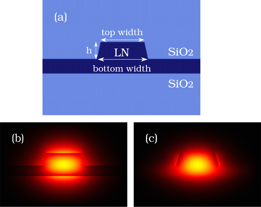
A mode solver was used to determine the dimensions of a single mode ridge waveguide in LNOI. The design of the waveguide includes the following parameters: ridge height, bottom width, top width, refractive indices of the waveguide and claddings, and film thickness. Figure 1(a) shows a typical cross-section of a z-cut ridge waveguide with SiO2 cladding.

The difference in the waveguide dimensions at the top and bottom of the ridge is due to the sidewall angle introduced by the etching process. LNOI waveguides support both TE and TM polarization and the electromagnetic field distribution is displayed in fig. 1(b) and fig. 1(c) for TE and TM modes.
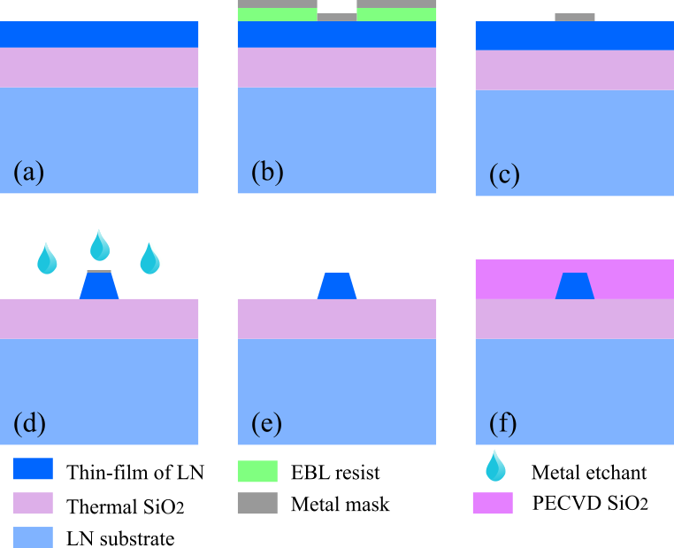
The fabrication process implemented to realize the ultra-low loss photonic circuits is shown in fig. 2. The raw sample is a thick z-cut LN film on top of thick buried SiO2 layer supported by a single-crystal z-cut LN substrate; the LNOI wafer was fabricated by Nanoln using the smart-cut technique. We use an optimized lift-off technique to define the circuit pattern and then transfer it to the substrate using RIE. In the first step of the fabrication process, shown in fig. 2, the positive resist is patterned by electron-beam lithography (EBL) to define the mask; the width of patterned structures is . The next step consists of metal (Cr) film deposition using an electron beam evaporator, and then lift-off is performed in either acetone or an NMP-based solution. The thickness of the metal layer is optimized to the selectivity of the etching process and depends on the desired etch depth. The chip is then etched in a mix of fluorine and argon plasma allowing smooth and near vertical sidewalls due to the combination of plasma chemical etching and physical sputtering. The metal mask is then removed via wet etching and the final structure cladded with SiO2. The top cladding minimizes the scattering loss induced by the sidewall roughness, facilitates further packaging processes (dicing and CMP polishing) of the final device, and protects the fragile structure from damage.

III Results
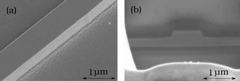
The fabricated structures were investigated using optical microscope, surface profilometer, scanning electron microscope (SEM), atomic force microscopy (AFM) and focused ion beam (FIB). The low roughness resulting by our fabrication process is shown in fig. 3(a), AFM was used to confirm the RMS. The ridge waveguide cross-section, obtained by focused ion beam milling, shows a sidewall angle of and an etch depth of , approximately half the film thickness fig. 3(b).

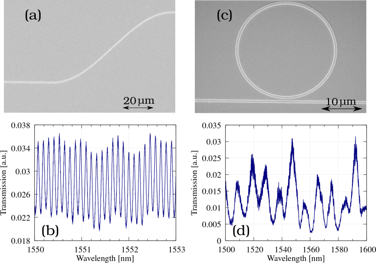
The optical loss characterization of a s-bend waveguide (shown in fig. 4(a)) is performed using the Fabry-Perot (FP) loss measurement technique Regener and Sohler (1985). The bend is used to reduce direct laser light coupling between input and output fibres. Laser light at wavelength is coupled into and out of the polished facets of the waveguide using polarization maintaining (PM) lensed fibers with a mode field diameter of . The total input and output coupling and propagation loss is for a long chip. The optical transmission spectrum is shown in fig. 4(b). The accurate estimation of the waveguide’s propagation loss via the FP technique requires the effective index of the waveguide, which can be found by the free spectral range (FSR) of a ring resonator of known dimensions. For this purpose, we designed and characterized a microring resonator, shown in fig. 4(c), and the optical transmission spectrum is reported in fig. 4(d). The low quality factor of the ring reported here is due to the significant bending loss resulting from the small radius of the ring. High quality factor ring resonators can be easily designed and fabricated by increasing the bend radius.
The effective index , is obtained using the measured FSR = () for TE (TM), ring radius R = and , where the coupling length C = . The result is = 2.00 (2.05) for TE (TM) polarization, which is in good agreement with our FDTD mode solver simulation. The propagation loss is calculate to be dB/cm for TE (TM) polarization. The error is calculated from the standard deviation of the fringe’s noise.

IV Discussion
The transmission measurements show that the optical losses are dominated by the mode mismatch between fiber and waveguide. To improve the coupling efficiency, inverse tapers or grating couplers can be used—the near-vertical angle of our waveguides enables the fabrication of these photonic components. Our sidewall angle of in LNOI waveguides is a significant improvement over previously reported Wang et al. (2016b); Liang et al. (2017) and close to commercially available waveguides in other platforms. Furthermore, to our knowledge, this is the first single mode waveguide reported in z-cut LNOI fabricated via RIE, and the measured sidewall roughness of RMS is the lowest reported to date in this material. Both sidewall angle and roughness can be further improved by increasing the ratio of chemical etching over physical sputtering.
While LNOI photonic components demonstrated here exhibit ultra-low optical propagation loss, the relatively shallow etching depth results in weak mode confinement, which sets a limit to the minimum bend radius achievable, hence limiting the circuit complexity. By increasing the etch depth, we expect to achieve high component density while preserving low propagation loss, which is comparable to AlN and SiNChi Xiong and Tang (2012).
V Conclusion
We have reported the fabrication of ultra-low loss single mode waveguides at telecom wavelength, lower than commercially available Si and SiN photonic platforms. The key advantage of using LNOI over Si and SiN is the second-order nonlinearity (not present in these materials due to the centrosymmetry of their crystalline structures) which enables the implementation of frequency converters, ultra-fast and lossless switches, as well as single photon sources for quantum technology. Future work will focus on the optimization of the process on x-cut LNOI, which can simplify the poling process, and MgO:LNOI, which has 170x higher optical damage threshold than undoped LN, and can support high power wavelength conversion applications.
Funding
Australian Research Council Centre for Quantum Computation and Communication Technology CE170100012; Australian Research Council Discovery Early Career Researcher Award, Project No. DE140101700; RMIT University Vice-Chancellors Senior Research Fellowship.
Acknowledgements
The authors acknowledge Andreas Boes for technical support. This work was performed in part at the Melbourne Centre for Nanofabrication (MCN) in the Victorian Node of the Australian National Fabrication Facility (ANFF) and the Nanolab at Swinburne University of Technology. The authors acknowledge the facilities, and the scientific and technical assistance, of the Australian Microscopy & Microanalysis Research Facility at RMIT University.
References
- Volz et al. (2012) T. Volz, A. Reinhard, M. Winger, A. Badolato, K. J. Hennessy, E. L. Hu, and A. Imamoglu, Nature Photonics 6, 605 (2012).
- Wang et al. (2016a) C. Wang, X. Xiong, N. Andrade, V. Venkataraman, X.-F. Ren, G.-C. Guo, and M. Lončar, SPIE/COS Photonics Asia 10029, 100290Z (2016a).
- Geiss et al. (2015) R. Geiss, S. Saravi, A. Sergeyev, S. Diziain, F. Setzpfandt, F. Schrempel, R. Grange, E.-B. Kley, A. Tünnermann, and T. Pertsch, Optics letters 40, 2715 (2015).
- Halldorsson et al. (2010) J. Halldorsson, N. B. Arnfinnsdottir, A. B. Jonsdottir, B. Agnarsson, and K. Leosson, Opt. Express 18, 16217 (2010).
- Shadbolt et al. (2012) P. G. Shadbolt, M. R. Verde, A. Peruzzo, A. Politi, A. Laing, M. Lobino, J. C. F. Matthews, M. G. Thompson, and J. L. O’Brien, Nature Photonics 6, 45 (2012).
- Alibart et al. (2016) O. Alibart, V. D’Auria, M. De Micheli, F. Doutre, F. Kaiser, L. Labonté, T. Lunghi, É. Picholle, and S. Tanzilli, Journal of Optics 18, 104001 (2016).
- Vaziri et al. (2002) A. Vaziri, G. Weihs, and A. Zeilinger, Phys. Rev. Lett. 89, 240401 (2002).
- Qianfan Xu1 and Lipson1 (2005) S. P. Qianfan Xu1, Bradley Schmidt1 and M. Lipson1, Nature 435, 325 (2005).
- Stabile et al. (2016) R. Stabile, P. DasMahapatra, and K. Williams, in Optical Fiber Communication Conference (Optical Society of America, 2016) p. Th1C.3.
- Bauters et al. (2011) J. F. Bauters, M. J. R. Heck, D. John, D. Dai, M.-C. Tien, J. S. Barton, A. Leinse, R. G. Heideman, D. J. Blumenthal, and J. E. Bowers, Opt. Express 19, 3163 (2011).
- Dietrich et al. (2016) C. P. Dietrich, A. Fiore, M. G. Thompson, M. Kamp, and S. Höfling, Laser & Photonics Reviews 10, 870 (2016).
- Chi Xiong and Tang (2012) W. H. P. P. Chi Xiong and H. X. Tang, Nano letters 12, 3562 (2012).
- Mayer et al. (2016) A. S. Mayer, C. R. Phillips, C. Langrock, A. Klenner, A. R. Johnson, K. Luke, Y. Okawachi, M. Lipson, A. L. Gaeta, M. M. Fejer, and U. Keller, Phys. Rev. Applied 6, 054009 (2016).
- Sohler (2000) W. Sohler, in Conference Digest. 2000 Conference on Lasers and Electro-Optics Europe (Cat. No.00TH8505) (2000) pp. 1 pp.–.
- Janner et al. (2009) D. Janner, D. Tulli, M. García-Granda, M. Belmonte, and V. Pruneri, Laser & Photonics Reviews 3, 301 (2009).
- Stepanenko et al. (2014) O. Stepanenko, E. Quillier, H. Tronche, P. Baldi, and M. De Micheli, IEEE Photonics Thechnology Letters 26, 1557 (2014).
- Hu et al. (2006) H. Hu, A. P. Milenin, R. B. Wehrspohn, H. Hermann, and W. Sohler, Journal of Vacuum Science & Technology A: Vacuum, Surfaces, and Films 24, 1012 (2006).
- Rabiei et al. (2013) P. Rabiei, J. Ma, S. Khan, J. Chiles, and S. Fathpour, Optics Express 21, 25573 (2013).
- Witmer et al. (2016) J. D. Witmer, J. A. Valery, P. Arrangoiz-Arriola, C. J. Sarabalis, J. T. Hill, and A. H. Safavi-Naeini, arXiv:1612.02421 (2016).
- Jin et al. (2016) S. Jin, L. Xu, H. Zhang, and Y. Li, IEEE Photonics Technology Letters 28, 736 (2016).
- Chang et al. (2017) L. Chang, M. H. P. Pfeiffer, N. Volet, M. Zervas, J. D. Peters, C. L. Manganelli, E. J. Stanton, Y. Li, T. J. Kippenberg, and J. E. Bowers, Opt. Lett. 42, 803 (2017).
- Volk et al. (2016) M. F. Volk, S. Suntsov, C. E. Rueter, and D. Kip, Optics Express 24, 1386 (2016).
- Takigawa et al. (2014) R. Takigawa, E. Higurashi, T. Kawanishi, and T. Asano, Optics Express 22, 27733 (2014).
- Poberaj et al. (2012) G. Poberaj, H. Hu, W. Sohler, and P. Günter, Laser & Photonics Reviews 6, 488 (2012).
- Wang et al. (2016b) C. Wang, X. Xiong, N. Andrade, V. Venkataraman, X.-F. Ren, G.-C. Guo, and M. Lončar, Optics Express 25, 6963 (2016b).
- Hu et al. (2009) H. Hu, R. Ricken, and W. Sohler, Opt. Express 17, 24261 (2009).
- Wang et al. (2014) C. Wang, M. J. Burek, Z. Lin, H. A. Atikian, V. Venkataraman, I.-C. Huang, P. Stark, and M. Lončar, Opt. Express 22, 30924 (2014).
- Hu et al. (2007) H. Hu, R. Ricken, W. Sohler, and R. B. Wehrspohn, Ieee Photonics Technology Letters 19, 417 (2007).
- Regener and Sohler (1985) R. Regener and W. Sohler, Applied Physics B 36, 143 (1985).
- Liang et al. (2017) H. Liang, R. Luo, Y. He, H. Jiang, and Q. Lin, arXiv:1706.08904 (2017).