This manuscript was accepted by Appl. Phys. Lett.
The citation for the published article is C. Barth, et al., Appl. Phys. Lett. 111, 031111 (2017).
Click here to see the published version: http://dx.doi.org/10.1063/1.4995229.
Increased Fluorescence of PbS Quantum Dots in Photonic Crystals by Excitation Enhancement
Abstract
We report on enhanced fluorescence of lead sulfide quantum dots interacting with leaky modes of slab-type silicon photonic crystals. The photonic crystal slabs were fabricated supporting leaky modes in the near infrared wavelength range. Lead sulfite quantum dots which are resonant the same spectral range were prepared in a thin layer above the slab. We selectively excited the leaky modes by tuning wavelength and angle of incidence of the laser source and measured distinct resonances of enhanced fluorescence. By an appropriate experiment design, we ruled out directional light extraction effects and determined the impact of enhanced excitation. Three-dimensional numerical simulations consistently explain the experimental findings by strong near-field enhancements in the vicinity of the photonic crystal surface. Our study provides a basis for systematic tailoring of photonic crystals used in biological applications such as biosensing and single molecule detection, as well as quantum dot solar cells and spectral conversion applications.
Excitation and emission of fluorescent species can largely be affected by leaky modes of photonic crystals (PhCs). PhCs can be designed with specifically tailored optical propertiesJoannopoulos et al. (2008) and have been intensely studied to improve systems that feature light emission, such as light-emitting diodes (LEDs)Fan et al. (1997); Wiesmann et al. (2009) and biosensorsCunningham et al. (2016). Especially in the life-sciences, the applications range from photonic crystal enhanced microscopy and single molecule detection to enhanced live cell imaging, DNA sequencing and gene expressionCunningham et al. (2016); Block et al. (2009); Ganesh et al. (2008a); Threm, Nazirizadeh, and Gerken (2012). Two processes can increase the light yield: (1) excitation enhancement by generating increased near-fields in the absorption wavelength range of the emitters, and (2) extraction enhancement by providing leaky-mode channels to improve the out-coupling of the fluorescent lightBoroditsky et al. (1999).
Extraction enhancement has not only been demonstrated for LEDs, but for nitrogen-vacancy centers in diamondOndič et al. (2011a), DNA microarraysBlock et al. (2009), moleculesGanesh et al. (2008b); Mathias, Ganesh, and Cunningham (2008) and quantum dots (QDs)Ryu et al. (2001); Ondič et al. (2012, 2013); Ganesh et al. (2007). Inducing extraction enhancement with PhCs has been demonstrated several times, both for intrinsic fluorescence of the PhC itselfOndič et al. (2011b, a) and for QDs embedded into the PhCGanesh et al. (2008b); Ondič et al. (2013) or on the PhC surfaceOndič et al. (2012). Extraction enhancement effects cause strong directional features of the emitted radiation which depend on the scattering angles of the involved leaky modesGanesh et al. (2008b); Ondič et al. (2012).
By excitation enhancement a significant increase in fluorescence of emitting species is expected in the vicinity of the PhC surface since the near-field energies of leaky modes can be orders of magnitude higher compared to the incident fieldBecker et al. (2014). In this way, PhC structures were applied to increase the efficiency of quantum dot solar cellsAdachi et al. (2013); Kim et al. (2013) and are shown to increase the quantum yield of up-conversion devicesSu et al. (2013); Zhang et al. (2010); Hofmann et al. (2016). PhC-induced excitation enhancement of fluorescent QDs was shown for individual modes or overlaid with directional extraction enhancement effectsGanesh et al. (2007, 2008a). However, an identification of modes exhibiting strong near-field energy densities and the knowledge of the exact 3D spatial distribution in a defined volume is of great importance for enhanced light excitation and emission independent of directional characteristics, e.g. in biosensing, quantum dot solar cells and up-conversion devices.
In this study, we experimentally map the integrated omnidirectional fluorescence of lead sulfide (PbS) QDs interacting with leaky modes of a silicon photonic crystal slab by using an angle- and excitation wavelength-resolved setup. Directional characteristics of light extraction are eliminated by placement of the sample inside an integrating sphere, hence allowing a pure determination of excitation enhancement effects. By using finite element simulations, the spectral position of the modes, as well as respective enhancement factors of the electric field energy density are calculated. The comparison of experiment and simulations enables us to explain the experimental fluorescence enhancement features by leaky modes exhibiting a large local electric field energy density.
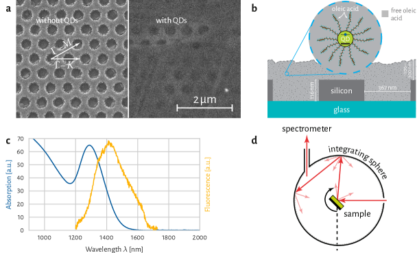
In order to realize a platform with increased electromagnetic near-fields, a silicon PhC slab on glass with a hexagonal lattice of cylindrical air holes is prepared (pitch: , layer thickness: , hole radius: ) using a process based on nanoimprint lithography, physical vapor deposition of silicon and solid phase crystallizationBecker et al. (2014); Barth, Burger, and Becker (2016). Figure 1(a, left) shows a scanning electron microscope image of the PhC with the two polar angle directions corresponding to the and paths between the high-symmetry points of the irreducible Brillouin zone. Subsequently, the PhCs are covered with spherical PbS QDs with a diameter of (manufacturer: CAN GmbH) using the convective assembly techniqueKraus et al. (2007) – a high accuracy process that distributes the QDs evenly across the sample (Fig. 1(a, right)). They are originally solved in toluene and their surface is shielded by an oleic acid ligand (the toluene is removed in the covering process). We note that we value the thickness of the QD-oleic acid layer based on SEM images to range from about to about . Figure 1(b) shows a sketch of the complete system in cross section after the particle assembly process. The absorption properties (blue) of the QDs as well as the fluorescence peak (orange) are shown in Fig. 1(c). These QDs can be pumped efficiently in a large spectral range from the visible up to about , while the fluorescence peak is centered at about . The fluorescence is measured by placing the samples inside an integrating sphere with diameter (Fig. 1(d)). For excitation a tunable laser source with a wavelength range of to is used (SACHER Lion Series) with linear polarization and a line width of . A fiber-coupled output port guides the light to the spectrometer (Ocean Optics) after passing an edge filter to suppress the excitation laser radiation. In order to vary the incident angle the sample is rotated inside the sphere. For further details on the experimental setup please see Fig. S1 in the Supplementary Material. Due to the usage of an integrated sphere the fluorescence measurement is independent of directional effects of the light emitted by the quantum dots. We have further checked that resonantly enhanced emission does not play a quantitative role in our experimental setup by measuring the spectral distribution of emitted light: this spectrum does not depend on the presence of the PhC.
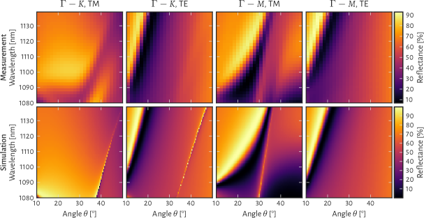
The fluorescence of the PbS QDs can be enhanced by an interaction with the leaky modes of the PhC. Therefore, leaky modes of the PhC were identified by angular- and wavelength-resolved reflectance measurements using a PerkinElmer Lambda 950 spectrometer with automated reflectance/transmittance analyzer supplement. Resonant features in the reflectance spectra can be attributed to the coupling of incident light to the photonic bands of the PhCAstratov et al. (1999). Figure 2 (upper row) shows the measured reflectance properties of the silicon PhC slabs for the four combinations of sample orientation (corresponding to and ) and source polarization (transversal electric, TE, and transversal magnetic, TM). We observe reflectance values of almost up to more than , indicating the presence of photonic bands. We decided to use a wavelength range of for the excitation (marked in Fig. 2). In this range, (1) the QDs show a considerable absorption, (2) do not show a fluorescence themselves and (3) the absorption of the silicon is low – which would deteriorate near-field enhancement effectsBecker et al. (2014). Notably, there are only a few well-isolated bands in the excitation wavelength regime which facilitates the interpretation of subsequent fluorescence measurements. For simulations we use a time-harmonic finite-element Maxwell solver (JCMsuitePomplun et al. (2007)) on a 2D-periodic unstructured, prismatoidal mesh of the unit cell of the hexagonal sample structure consisting of a glass subspace and a silicon-hole-layer on top. Each simulation uses a distinct plane wave excitation corresponding to the direction of incidence, wavelength and polarization. We assure numerical convergence by comparing the derived quantities to those calculated in a highly accurate reference solution, guaranteeing an accuracy of . Optical constants are taken from tabulated valuesPalik (1985) for glass and silicon, considering all the significant physical effects including dispersion and absorption. The numerically obtained reflectance maps calculated using Fourier transforms on the required domain boundaries are shown in the lower row of Fig. 2. A comparison with the measured reflectance maps allowed us to reconstruct the exact geometrical parameters of the produced sample using the reduced basis methodHammerschmidt et al. (2016). While a first guess from experimental scanning electron microscopic images yielded a silicon thickness of and a hole diameter of , the numerical reconstruction generated more exact values with a silicon thickness of , a hole diameter of and a lattice pitch of . The maps agree excellently with the measured results in the whole spectral range. We reason from this comparison that the numerical model gives accurate predictions for the fabricated sample.
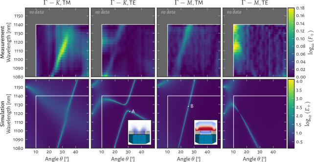
We then measured the fluorescence of the PbS-QDs on the PhC surface experimentally in an angle- and wavelength-resolved setup (Fig. 1(d)) in a region of high QD-layer thickness in order to reach a sufficient signal (i.e. ). To achieve the fluorescence enhancement maps depicted in Fig. 3 (top row), each measured spectrum was first integrated over the fluorescence peak from to and normalized to the measured incident laser power and the absorption profile of the quantum dots. We further characterized the dependence on the incident angle of the integrating sphere using a planar reference (i.e. the PbS/oleic acid system on an unpatterned silicon film of the same thickness as the PhC slab) and corrected the results correspondingly. With these corrections and subsequent background filtering, we find maps for the actual fluorescence of the QDs. We find a minimal estimate for the fluorescence enhancement shown in Fig. 3 (top row) by dividing by the minimal value in each of the measurement windows. We observe clear and sharp features of enhanced fluorescence with a maximum enhancement factor of , i.e. an increase of roughly . An isolated steep band of enhanced fluorescence is observed for TM polarized light. For TE polarized light also distinct features appear in the fluorescence enhancement maps.
For a better understanding, we compare these experimentally determined fluorescence results to numerically obtained field energy enhancement maps in the bottom row of Fig. 3 (using the same logarithmic color scale for all maps). Please note that upper and lower row do not show the same physical quantity. For the determination of the electric field energy enhancement , we integrate the electric field energy density distribution over the superspace volume -– defined by the PhC hole and a layer above the silicon – and normalize it to the energy of the incident plane wave source in the same volume . We numerically treat the PbS/oleic acid system in this superspace volume as an infinite space of an average refractive index material with , estimated by thermo gravimetric mass fraction analysis and the respective densities and refractive indices of both materials in the wavelength range of interest (, ). In the simulations, we observe field energy enhancement values of up to correlated with peak width (FWHM) of . Such a resolution is not reached in the experiment due to the laser bandwidth of . Geometrical imperfections of the PhC further broaden the leaky mode resonances. This partly explains why large simulated electric field enhancement factors of up to only result in fluorescence enhancements of . A further reason might be the fact, that the thickness of the QD containing layer is much larger than the spatial extend of the modes. Exemplary, two numerical field energy distributions are shown as insets in Fig. 3. The leaky mode (A) is located very close to the PhC surface such that only a small fraction of the quantum dots located closely on the photonic crystal surface is exposed to the enhanced fields. In addition, the corresponding peak has a high Q-factor of (i.e. a FWHM of ) which causes an ineffective excitation with a laser bandwidth of (see the supplementary material, Tab. S1, for additional Q-factors and discussion). Hence, no fluorescence enhancement is visible in the experiment. However, resonance (B) exhibits a much larger extent and overlap with the QDs which can be clearly correlated with a measurable fluorescence enhancement. This is also supported by the Q-factor of (FWHM), which fits the laser bandwidth much more accurately. A larger amount of simulated field energy distributions is shown in Fig. S2 of the supplementary material. Nevertheless, the qualitative agreement of the position of the resonances regarding wavelength and angle of incidence is excellent: note the almost isolated steep band of high field energy enhancement occurring in the two maps with TM polarized light, which is also clearly visible in the measurement with a very good accordance in their gradient angles and spectral positions. The TE-cases feature bands that show anti-crossing behavior in the simulationsBarth, Burger, and Becker (2016) which can also partly be observed in the experiment. We explain the distinct differences between experimental and numerical results in the TE-cases by Q-factor mismatches and the above mentioned insufficient overlap of leaky mode and QDs, which is in fact obvious from a 3D field energy distribution analysis.
In conclusion, we measured increased fluorescence by excitation enhancement of PbS QDs on the surface of a hexagonal-lattice silicon PhC slab with a maximum enhancement of . Directional extraction characteristics were eliminated by an appropriate experimental setup allowing for an undisguised determination of excitation enhancement effects. We explained our findings by the interaction of the QDs with leaky modes exhibiting large field energy enhancement values close to the PhC surface. A numerical analysis yielded the 3-dimensional distribution of the involved leaky modes and their spatial overlap with the QDs well explaining the presence or the absence of enhanced fluorescence. We conclude that a systematic placement of emitting species directly on the photonic crystal surface enables to increase the fluorescence enhancement factors. The knowledge of strength and spatial distribution of light interacting with PhC leaky modes will be of importance for excitation enhanced future devices in the fields of biosensors, photochemistry, up-conversion and QD solar cells.
Supplementary material
See supplementary material for details on the fluorescence enhancement measurement setup, additional simulated 3-dimensional electric field energy distributions and a Q-factor analysis.
Acknowledgements.
The authors thank David Eisenhauer, Grit Köppel, Bernd Rech and Klaus Jäger from Helmholtz-Zentrum Berlin for support at sample fabrication and useful discussions. The German Federal Ministry of Education and Research is acknowledged for funding the research activities of the Nano-SIPPE group within the program NanoMatFutur (No. 03X5520). Further we acknowledge support by the Einstein Foundation Berlin through ECMath within subproject OT9. Parts of the results were obtained at the Berlin Joint Lab for Optical Simulations for Energy Research (BerOSE) of Helmholtz-Zentrum Berlin für Materialien und Energie, Zuse Institute Berlin and Freie Universität Berlin.References
- Joannopoulos et al. (2008) J. D. Joannopoulos, S. G. Johnson, J. N. Winn, and R. D. Meade, Princet. Univ., 2nd ed., Vol. 2 (Princeton University Press, 2008).
- Fan et al. (1997) S. Fan, P. R. Villeneuve, J. D. Joannopoulos, and E. F. Schubert, “High Extraction Efficiency of Spontaneous Emission from Slabs of Photonic Crystals,” Phys. Rev. Lett. 78, 3294–3297 (1997).
- Wiesmann et al. (2009) C. Wiesmann, K. Bergenek, N. Linder, and U. Schwarz, “Photonic crystal LEDs - designing light extraction,” Laser Photonics Rev. 3, 262–286 (2009).
- Cunningham et al. (2016) B. T. Cunningham, M. Zhang, Y. Zhuo, L. Kwon, and C. Race, “Recent Advances in Biosensing With Photonic Crystal Surfaces: A Review,” IEEE Sens. J. 16, 3349–3366 (2016).
- Block et al. (2009) I. D. Block, P. C. Mathias, N. Ganesh, S. I. Jones, B. R. Dorvel, V. Chaudhery, L. O. Vodkin, R. Bashir, and B. T. Cunningham, “A detection instrument for enhanced-fluorescence and label-free imaging on photonic crystal surfaces,” Opt. Express 17, 13222 (2009).
- Ganesh et al. (2008a) N. Ganesh, P. C. Mathias, W. Zhang, and B. T. Cunningham, “Distance dependence of fluorescence enhancement from photonic crystal surfaces,” J. Appl. Phys. 103, 083104 (2008a).
- Threm, Nazirizadeh, and Gerken (2012) D. Threm, Y. Nazirizadeh, and M. Gerken, “Photonic crystal biosensors towards on-chip integration,” J. Biophotonics 5, 601–616 (2012).
- Boroditsky et al. (1999) M. Boroditsky, R. Vrijen, T. Krauss, R. Coccioli, R. Bhat, and E. Yablonovitch, “Spontaneous emission extraction and Purcell enhancement from thin-film 2-D photonic crystals,” J. Light. Technol. 17, 2096–2112 (1999).
- Ondič et al. (2011a) L. Ondič, K. Kůsová, O. Cibulka, I. Pelant, K. Dohnalová, B. Rezek, O. Babchenko, A. Kromka, and N. Ganesh, “Enhanced photoluminescence extraction efficiency from a diamond photonic crystal via leaky modes,” New J. Phys. 13, 063005 (2011a).
- Ganesh et al. (2008b) N. Ganesh, I. D. Block, P. C. Mathias, W. Zhang, E. Chow, V. Malyarchuk, and B. T. Cunningham, “Leaky-mode assisted fluorescence extraction: application to fluorescence enhancement biosensors.” Opt. Express 16, 21626–21640 (2008b).
- Mathias, Ganesh, and Cunningham (2008) P. C. Mathias, N. Ganesh, and B. T. Cunningham, “Application of Photonic Crystal Enhanced Fluorescence to a Cytokine Immunoassay,” Anal. Chem. 80, 9013–9020 (2008).
- Ryu et al. (2001) H. Y. Ryu, Y. H. Lee, R. L. Sellin, and D. Bimberg, “Over 30-fold enhancement of light extraction from free-standing photonic crystal slabs with InGaAs quantum dots at low temperature,” Appl. Phys. Lett. 79, 3573 (2001).
- Ondič et al. (2012) L. Ondič, O. Babchenko, M. Varga, A. Kromka, J. Čtyroký, and I. Pelant, “Diamond photonic crystal slab: Leaky modes and modified photoluminescence emission of surface-deposited quantum dots,” Sci. Rep. 2, 914 (2012).
- Ondič et al. (2013) L. Ondič, M. Varga, K. Hruška, A. Kromka, K. Herynková, B. Hönerlage, and I. Pelant, “Two-dimensional photonic crystal slab with embedded silicon nanocrystals: Efficient photoluminescence extraction,” Appl. Phys. Lett. 102, 251111 (2013).
- Ganesh et al. (2007) N. Ganesh, W. Zhang, P. C. Mathias, E. Chow, J. a. N. T. Soares, V. Malyarchuk, A. D. Smith, and B. T. Cunningham, “Enhanced fluorescence emission from quantum dots on a photonic crystal surface,” Nat. Nanotechnol. 2, 515–520 (2007).
- Ondič et al. (2011b) L. Ondič, K. Dohnalova,́ M. Ledinsky,́ A. Kromka, O. Babchenko, and B. Rezek, “Effective Extraction of Photoluminescence from a Diamond Layer with a Photonic Crystal,” ACS Nano 5, 346–350 (2011b).
- Becker et al. (2014) C. Becker, P. Wyss, D. Eisenhauer, J. Probst, V. Preidel, M. Hammerschmidt, and S. Burger, “ silicon photonic crystal slabs on glass and plastic foil exhibiting broadband absorption and high-intensity near-fields,” Sci. Rep. 4, 5886 (2014).
- Adachi et al. (2013) M. M. Adachi, A. J. Labelle, S. M. Thon, X. Lan, S. Hoogland, and E. H. Sargent, “Broadband solar absorption enhancement via periodic nanostructuring of electrodes,” Sci. Rep. 3, 2928 (2013).
- Kim et al. (2013) S. Kim, J. K. Kim, J. Gao, J. H. Song, H. J. An, T.-s. You, T.-S. Lee, J.-R. Jeong, E.-S. Lee, J.-H. Jeong, M. C. Beard, and S. Jeong, “Lead Sulfide Nanocrystal Quantum Dot Solar Cells with Trenched ZnO Fabricated via Nanoimprinting,” ACS Appl. Mater. Interfaces 5, 3803–3808 (2013).
- Su et al. (2013) L. T. Su, S. K. Karuturi, J. Luo, L. Liu, X. Liu, J. Guo, T. C. Sum, R. Deng, H. J. Fan, X. Liu, and A. I. Y. Tok, “Photon Upconversion in Hetero-nanostructured Photoanodes for Enhanced Near-Infrared Light Harvesting,” Adv. Mater. 25, 1603–1607 (2013).
- Zhang et al. (2010) F. Zhang, Y. Deng, Y. Shi, R. Zhang, and D. Zhao, “Photoluminescence modification in upconversion rare-earth fluoride nanocrystal array constructed photonic crystals,” J. Mater. Chem. 20, 3895 (2010).
- Hofmann et al. (2016) C. L. M. Hofmann, B. Herter, S. Fischer, J. Gutmann, and J. C. Goldschmidt, “Upconversion in a Bragg structure: photonic effects of a modified local density of states and irradiance on luminescence and upconversion quantum yield,” Opt. Express 24, 14895 (2016).
- Barth, Burger, and Becker (2016) C. Barth, S. Burger, and C. Becker, “Symmetry-dependency of anticrossing phenomena in slab-type photonic crystals,” Opt. Express 24, 10931 (2016).
- Kraus et al. (2007) T. Kraus, L. Malaquin, H. Schmid, W. Riess, N. D. Spencer, and H. Wolf, “Nanoparticle printing with single-particle resolution.” Nat. Nanotechnol. 2, 570–6 (2007).
- Astratov et al. (1999) V. N. Astratov, D. M. Whittaker, I. S. Culshaw, R. M. Stevenson, M. S. Skolnick, T. F. Krauss, and R. M. De La Rue, “Photonic band-structure effects in the reflectivity of periodically patterned waveguides,” Phys. Rev. B 60, R16255–R16258 (1999).
- Pomplun et al. (2007) J. Pomplun, S. Burger, L. Zschiedrich, and F. Schmidt, “Adaptive finite element method for simulation of optical nano structures,” Phys. status solidi b 244, 3419–3434 (2007), arXiv:0711.2149 .
- Palik (1985) E. D. Palik, Handb. Opt. Constants Solids (Elsevier, 1985).
- Hammerschmidt et al. (2016) M. Hammerschmidt, C. Barth, J. Pomplun, S. Burger, C. Becker, and F. Schmidt, “Reconstruction of photonic crystal geometries using a reduced basis method for nonlinear outputs,” Proc. SPIE 9756, 97561R (2016).