Topological Semimetals Studied by Ab Initio Calculations
Abstract
In topological semimetals such as Weyl, Dirac, and nodal-line semimetals, the band gap closes at points or along lines in space which are not necessarily located at high-symmetry positions in the Brillouin zone. Therefore, it is not straightforward to find these topological semimetals by ab initio calculations because the band structure is usually calculated only along high-symmetry lines. In this paper, we review recent studies on topological semimetals by ab initio calculations. We explain theoretical frameworks which can be used for the search for topological semimetal materials, and some numerical methods used in the ab initio calculations.
1 Introduction
Theoretical proposals of a topological insulator (TI) phase [1, 2, 3, 4, 5, 6] have triggered intensive studies on various types of topological states. In addition to a TI phase, there are various topological phases with a gap, such as an integer quantum Hall system [7], and a topological crystalline insulator [8]. They have characteristic surface or edge states, which manifest the topological nature of the bulk wave functions. Through the research on TIs, a new category of topological phases, called topological semimetals (topological metals), has been found in condensed matter physics. Degeneracy between conduction and valence bands usually occurs only at high-symmetry points or lines in space. In contrast, research on topological semimetals has shown us other possibilities for band degeneracies that originate from topology. In such topological semimetals, the band gap closes at generic points, and this closing of the gap originates from topological reasons.
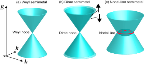
In Fig. 1, we show typical classes of three-dimensional (3D) topological semimetals. In Weyl semimetals (WSMs)[9, 10] [Fig. 1(a)], the bulk valence and conduction bands touch each other at isolated points called Weyl nodes, and around the Weyl nodes the bands form nondegenerate 3D Dirac cones. In spinful systems, i.e., when the spin-orbit coupling is nonzero, if both time-reversal (TR) and inversion symmetries are present, all states are doubly degenerate by the Kramers theorem. Therefore, a Weyl semimetal requires breaking of either inversion symmetry or TR symmetry. On the other hand, a topological semimetal having a Dirac cone with Kramers double degeneracy is realized when both inversion symmetry and TR symmetry are preserved. Such a semimetal is called a Dirac semimetal [12, 11] (Fig. 1(b)). Another type of topological metal called nodal-line semimetals (NLSs) [13, 14, 15, 16, 17, 18, 19, 20, 21, 22, 23]. is shown in Fig. 1(c), where the band gap closes along a loop in space. In these topological semimetals, the band gap closes at generic points in space, which originates from the interplay between the -space topology and symmetry. Because degeneracies in topological semimetals are not necessarily located at high-symmetry points in the Brillouin zone, an efficient and systematic search for topological semimetals is usually difficult. Moreover, such degeneracies occur at generic points; therefore, they may easily be overlooked in ab initio calculations, where the band structure is usually calculated only along high-symmetry lines. Thus, the search for topological semimetals has been an elusive issue.
In this paper, we first review basic properties of topological semimetals, and then review the ab initio approach to the material search and explorations of physical properties of topological semimetals. In Sect. 2, we review basic properties of WSMs and show some ab initio results for WSMs. We then give an overview of Dirac semimetals in Sect. 3. In Sect. 4, we explain the NLSs and give some examples such as calcium. Numerical methods for topological systems in ab initio calculations are explained in Sect. 5. We conclude this paper in Sect. 6.
2 Weyl Semimetals
2.1 Overview
In a WSM, [9, 26, 24, 25] the Weyl nodes have a topological nature. Namely, one can associate each Weyl node with a number , called a monopole charge for the Berry curvature in space[27, 9, 28]. The monopole charge is also called the helicity or chirality. This means that the degeneracy at a Weyl node cannot be lifted perturbatively. The monopole density , associated with the Berry curvature , is defined as
| (1) |
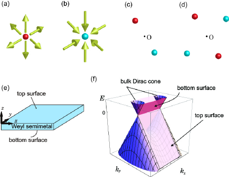
where is the periodic part of the th Bloch eigenfunction. One can prove that in general the monopole density is a superposition of functions with integer coefficients, (: integer), and this is the monopole charge at . The positions of the monopoles are the points where the th band touches other bands in terms of energy. In particular, the monopole charge at a Weyl node is either or , corresponding to a monopole (Fig. 2(a)) or an antimonopole (Fig. 2(b)), respectively. This is seen directly by using a simple 2-band Hamiltonian representing a Weyl node at , , where are constants and are the Pauli matrices; then, the monopole charges at the Weyl node for the upper band and lower band are calculated as , where is the determinant of the 33 matrix of . The Weyl nodes in three dimensions are topological and robust against perturbations owing to their monopole charges, unlike those in two dimensions.
We explain here the symmetry requirements of WSMs. WSMs appear only when either the TR symmetry or the inversion symmetry is broken. In WSMs with inversion symmetry but without TR symmetry, the monopole density is an odd function of , and the Weyl nodes distribute antisymmetrically in space (Fig. 2(c)). Similarly, in WSMs with TR symmetry but without inversion symmetry, the monopole density is an even function of , and the Weyl nodes distribute symmetrically in space. Since the sum of the monopole charges over the entire Brillouin zone is zero, the minimal configuration of Weyl nodes in this case contains four Weyl nodes, as shown in Fig. 2(d).
This topological property of Weyl nodes [29, 30, 9] necessitates the appearance of a surface Fermi surface forming an open arc, called a Fermi arc [10, 24, 25, 31, 32, 33], unlike usual Fermi surfaces, which are closed surfaces (in three dimensions) or closed loops (in two dimensions). The two end points of the Fermi arc are projections of the Weyl points, a monopole and an antimonopole, onto the surface Brillouin zone. The appearance of a surface Fermi arc is shown by introducing the Chern number in a two-dimensional slice of the three-dimensional Brillouin zone [10]. In a slab of a WSM (Fig. 2(e)), a typical form of the dispersion of bulk and surface states for the surface along the plane is shown in Fig. 2(f). Between the two bulk Dirac cones, there are two surface Fermi arcs, one on the top surface and the other on the bottom surface. These two Fermi arcs are both tangential to the bulk Dirac cones but have opposite dispersions and thus opposite velocities.
WSMs with broken TR symmetry have been proposed to include pyrochlore iridates [10], HgCr2Se4 [34], Co-based Heusler compounds [35], magnetic superlattices with a TI and a normal insulator (NI) [36, 37], and so on. Those with broken inversion symmetry include TaAs, BiTeI under high pressure[38], Te at high pressure[39], LaBi1-xSbxTe3, LuBi1-xSbxTe3 [38], transition-metal dichalcogenides [40, 41], SrSi2 [42], WTe2 [43], HgTexS1-x under strain [44], and superlattice with broken inversion symmetry [45]. In accordance with theoretical predictions [41, 46], TaAs and related materials have been experimentally established to be WSMs [50, 49, 51, 47, 48].
Weyl nodes are generally difficult to find in the 3D Brillouin zone because they are at general positions in space. Meanwhile, when the system breaks TR symmetry but preserves inversion symmetry, we can exploit a topological invariant to find a WSM phase [52, 53]. Let denote wavevectors satisfying modulo reciprocal vectors. They are called time-reversal invariant momenta (TRIM). The invariant is given by
| (2) |
where is the parity eigenvalue of the th occupied band at one ot the TRIM . The topological invariant takes a value of or . If , the energy bands have pairs of Weyl nodes, where is an integer [52, 53]. For example, ZrCo2Sn, which is a candidate magnetic WSM, has a nontrivial invariant [35]. However, this invariant cannot be defined in a system without inversion symmetry, leading to a further difficulty in determining whether the system is a WSM since Weyl nodes are generally difficult to find in the 3D Brillouin zone. In such inversion-asymmetric WSMs, the trajectories of the emergent Weyl nodes upon a continuous change in the system are related to the Fu–Kane–Mele invariant [54, 9], whose definition is similar to that of , as discussed later in this section. Studies on this relationship provide us with a new perspective on the search for semimetals through ab initio calculations.
2.2 Phase transition between topological insulators and Weyl semimetals
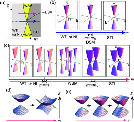
When the inversion symmetry is broken, there is a close relationship between TIs and WSMs in three dimensions. Namely, in 3D inversion-asymmetric systems, phase transitions between two phases with a different topological number are always accompanied by the WSM phase in between [9, 55]. We assume that the TR symmetry is preserved. Figure 3(a) shows a universal phase diagram for STI-WTI or STI-NI phase transitions, where is a parameter controlling the phase transition and is a parameter controlling the degree of inversion symmetry breaking. Here, STI and WTI stand for a strong TI and a weak TI, respectively. As seen from Fig. 3(a), the phase transition is different in the presence or absence of inversion symmetry. First, in inversion-symmetric systems, the gap can close only at TRIM, where the parity eigenvalues are exchanged at the gap closing (Fig. 3(b)); thereby, the topological numbers change, leading to a STI-WTI or STI-NI transition. At the band touching, the system is a Dirac semimetal (DSM). Such a phase transition is realized, for example, in TlBi(S1-xSe2)2 at around [56, 57]. Second, in inversion asymmetric cases, every state is nondegenerate except at TRIM. The gap can close only away from TRIM. Such gap closing always involves the creation of a pair of Weyl nodes [9, 55]. Because the Weyl nodes are either monopoles or antimonopoles, they can appear or disappear by pair creation/annihilation only. This gives robustness to the WSM phase; namely, as we change an external parameter which controls the topological phase transition, the WSM phase persists for a finite range of : . At the end value (), the pair creation (annihilation) of Weyl nodes occurs. These considerations lead to the phase diagram shown in Fig. 3(a).
The pattern of monopole-antimonopole pair creation and annihilation depends on the crystallographic symmetry. From Fig. 2(d), the minimal case involves two monopoles and two antimonopoles, as shown in Fig. 3(c). As we change the control parameter from the value for an insulating phase, two monopole-antimonopole pairs are created at first. As we change further, these monopoles and antimonopoles move in space, and eventually they annihilate pairwise. When the system has discrete rotational symmetry such as threefold or fourfold rotational symmetry, the minimal number of monopole-antimonopole pairs will be larger, as demonstrated in some systems [45]. In this phase transition from the WSM phase to the TI phase, the Fermi arcs in the WSM phase merge with each other to form a Dirac cone in the TI phase [32]. Here we emphasize the role of topology. The appearance of the WSM phase in three dimensions in a finite range in the phase diagram is due to the topological nature of Weyl nodes [55]. In contrast, in two dimensions, the NI-TI phase transition occurs directly, without the appearance of a WSM phase [9, 55]. This result has been shown by assuming no additional crystallographic symmetries. Furthermore, the result in Ref. 58 shows that this conclusion of the existence of the WSM phase in the phase transition holds true in general, whenever inversion symmetry is broken. One of the remarkable conclusions here is that an insulator-to-insulator (ITI) transition never occurs in inversion-asymmetric systems. This is in strong contrast with inversion-symmetric systems, where a transition between different topological phases always occurs as an ITI transition (i.e., at a single value of ).
Indeed, this NI-WSM-STI phase transition appears in various materials without inversion symmetry. We first apply this theory to BiTeI, whose space group is No.156 () and lacks inversion symmetry [59]. BiTeI is an NI at ambient pressure and has been proposed to become an STI at high pressure [61, 60]. Subsequently, ab initio calculations [38] showed the existence of a WSM phase between the NI and STI phases in a narrow window of pressure, which had been overlooked in earlier works [61, 60]. When the pressure is increased, the gap first closes at six S points on the A-H lines, and six pairs of Weyl nodes are created. Then the Weyl nodes move in space until they annihilate each other on mirror planes, leading to the STI phase [38]. The combination of all the trajectories of the Weyl nodes forms a loop around the TRIM point (A point), meaning that a band inversion occurs at the A point. This leads to a change in the topological number between the two bulk-insulating phases sandwiching the WSM phase [9, 55].
Other examples are LaBi1-xSbxTe3 and LuBi1-xSbxTe3, which have been proposed to show NI-WSM -TI phase transitions upon changing [38]. The space group is No.160 () and lacks inversion symmetry. By increasing , the band gap closes at six generic points, and Weyl nodes are created in pairs [38]. The resulting 12 Weyl nodes move in space, and they are then annihilated pairwise to open a bulk gap, and the topological number is changed from that in the low- phase [38].
2.3 Closing of a gap in inversion-asymmetric systems
Next, motivated by the universal phase diagram (Fig. 3(a)), we can show a stronger conclusion that the closing of a gap of any inversion-asymmetric semiconductor (with spin-orbit coupling and TR symmetry) in three dimensions leads to either a WSM or an NLS [58], as we explain in the following. This is shown for all the space groups without inversion symmetry, and is widely applicable to various semiconductors without inversion symmetry.
To show this, we introduce a single parameter in the Hamiltonian, and assume that the change in does not change the system symmetry. We consider a Hamiltonian matrix representing the lowest conduction band and the highest valence band. Here, is a Bloch wavevector. We assume that for the system is an insulator, and that at the gap closes at a wavevector . Then to see what happens when exceeds , we expand the Hamiltonian in terms of and , and retain some of the lower-order terms. We consider all 138 space groups without inversion symmetry. For each space group, there are various high-symmetry points such as , , and . Each point is associated with a little group ( group), which leaves the point unchanged. Then the Hamiltonian is determined by the double-valued irreducible representations (irreps) [62] of the little group at . Let and denote the irreps of the lowest conduction band and the highest valence band, respectively.
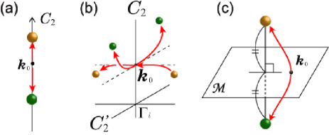
As the first example, we consider the case when the band gap closes at generic points in three dimensions. Such closing of the gap always accompanies the creation of a pair of Weyl nodes, as shown in Refs. 9 and 55. This occurs because Weyl nodes have quantized monopole charges for the -space Berry curvature; this topological property allows the creation of pairs of Weyl nodes with and . Furthermore, if there is additional symmetry, the gap closing becomes more involved. For example, suppose the little group consists only of the twofold () symmetry. Then there are two one-dimensional (1D) irreps of the eigenvalues with opposite signs. For , the gap can close and the closing of the gap accompanies the creation of a pair of Weyl nodes. When is increased, the two Weyl nodes (a monopole and an antimonopole) move along the axis, as shown in Fig. 4(a). On the other hand, when , the gap cannot close by changing because of level repulsion. In addition, when there are some additional symmetries such as , where stands for the TR operation and represents another twofold rotation, the gap can close when and the trajectory of the Weyl nodes is shown in Fig. 4(b). Next we consider the case with the little group consisting only of a mirror symmetry or a glide symmetry. There are two representations with opposite signs of mirror (or glide) eigenvalues. In the case , the gap can close, leading to the creation of a pair of Weyl nodes. The trajectory of the monopole and that of the antimonopole are mirror images to each other (Fig. 4(c)). On the other hand, for , the gap closes along a loop (i.e., nodal line) within the mirror plane in space, and the system is an NLS.
From this analysis, we conclude that there are only two possibilities after closing of the gap in inversion-asymmetric insulators with TR symmetry: NLSs (Fig. 3(d)) and WSMs (Fig. 3(e)). The space group, the wavevector at the gap closing, and the irreducible representations of the highest valence and lowest conduction bands uniquely determine which possibility is realized and where the gap-closing points or lines are located after the closing of the gap, as summarized in Ref. 58. In the NLSs, the highest valence and lowest conduction bands have different mirror eigenvalues. Remarkably, an ITI phase transition never occurs in any inversion asymmetric system, as we noted earlier.
2.4 Realization of materials
This universal result applies to all crystalline materials with spin-orbit coupling (SOC) and TR symmetry without inversion symmetry. We present some examples here. The first example is HgTexS1-x under strain, which has been shown to become a WSM [44]. It has a zincblende structure having the space group (No.216), and a strain along the [001] direction reduces the space group to (No.119). In this case, when is increased, the gap closes at four points on the -K lines, producing four pairs of Weyl nodes. The eight Weyl points then move within the plane with a further increase in , until they are mutually annihilated after rotation around the axis [44].
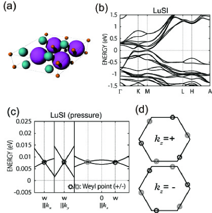
We can use the result in the previous subsection to search for topological semimetal materials. We start with any narrow-gap semiconductor without inversion symmetry, and close the gap by changing the system by, for example, applying pressure or by atomic substitution. Then, as we showed previously, the system becomes either a WSM or an NLS. As an example, we show LuSI as a WSM under pressure. The structure type of LuSI is GdSI (Fig. 5(a)) with the space group No.174 (). Figure 5(b) shows the electronic structure of LuSI, having a very narrow gap ( eV) near the M point. By applying pressure, the band gap first closes at six generic points on the plane. The system then becomes a WSM under pressure, having six monopoles and six antimonopoles at the same energy since they are related by symmetry, as shown in Fig. 5(c)).
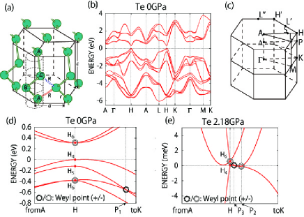
Another example is tellurium (Te) [39]. The crystal structure consists of 1D helical chains, as shown in Fig. 6(a). The unit cell contains three atoms in the same helical chain. When the helical chains are right-handed/left-handed, its space group is No.152 ()/No.154 (), and these two structures are mirror images of each other. Tellurium is a narrow gap semiconductor at ambient pressure. Figure 6(b) shows the band structures of Te at ambient pressure, and Fig. 6(c) shows the labels for high-symmetry points. The band gap in the +SO is eV for Te, which is in good agreement with the experimental value of eV [63, 64]. Both the bottom of the conduction band and top of the valence band are close to but slightly away from the H point in Te (Fig. 6(c)) [65]. At higher pressure, the gap closes and eventually a pair of Weyl nodes is produced at each of the four P points on the K-H lines, and the system becomes a WSM at 2.17–2.19 GPa (Fig. 6(e)). The P2 and P3 points are Weyl nodes between the valence and conduction bands. The Weyl nodes then move along the axes (K-H lines), as was confirmed by the ab initio calculation [39].
3 Dirac Semimetals
Materials having a linear dispersion with Kramers degeneracy at or near the Fermi energy are called Dirac semimetals. Thus, from the requirement for the Kramers degeneracy, inversion and TR symmetries are required for Dirac semimetals. Dirac semimetals have been proposed to include Na3Bi [12], Cd3As2 [11], -BiO2 [66], and so on, and they have been experimentally established in Na3Bi [67, 68] and Cd3As2 [69, 70]. The Dirac nodes can be regarded as a superposition of two Weyl nodes with monopole charges , i.e., a monopole and an antimonopole for the Berry curvature. Thus, by adding perturbation the gap can be opened [66] via monopole-antimonopole pair annihilation.
Thus, in real materials, one can always have such perturbation terms. Dirac nodes always have a gap if no other crystallographic symmetries are considered, and are not robust against perturbations. This is in strong contrast to Weyl nodes. The crystallographic symmetries required for stabilization of the Dirac semimetal phase have been discussed [71], and indeed such symmetries are present in the material examples mentioned above.
4 Nodal-Line Semimetal
As another example of topological semimetals, in an NLS [37, 13, 14, 15, 16, 17, 18, 19, 20, 21, 22, 23, 72], the band gap closes along a curve, called a nodal line, in space. Such a degeneracy along a nodal line cannot appear without a special reason, such as the symmetry or topology of the system. There are several mechanisms for the emergence of nodal lines. Among the various mechanisms of the emergence of nodal lines, we introduce two typical mechanisms: (A) mirror symmetry and (B) the Berry phase. In both cases, the nodal line forms a closed loop. In the following, we discuss the two cases (A) and (B) separately. In some materials the two mechanisms coexist, whereas in others the nodal line originates from only one of these mechanisms.
4.1 Nodal lines stemming from mirror symmetry
In case (A), the system should have a mirror symmetry or glide symmetry. When the mirror/glide operation and the Hamiltonian commute, they are simultaneously diagonalized. The eigenvalues of the mirror/glide operations depend on the situation, but they always have two values with opposite signs. For example, in spinless systems, the mirror eigenvalues are , originating from , and in spinful electronic systems, the mirror eigenvalues are . In all cases, the states on the mirror plane can be classified into two classes based on the mirror/glide eigenvalues. If the valence and conduction bands have different mirror/glide eigenvalues, then the two bands have no hybridization (i.e., no level repulsion) on the mirror/glide plane, even if the two bands approach and cross. This results in a degeneracy along a loop on the mirror/glide plane. This line-node degeneracy is protected by mirror/glide symmetry; once the mirror/glide symmetry is broken, the degeneracy is lifted in general.
Many materials have been proposed to belong to this class of NLSs. Dirac NLSs having Kramers degeneracy include carbon allotropes [15, 16], Cu3PdN [17, 18], Ca3P2 [19, 20], LaN [21], CaAgX (X=P, As) [22] and compressed black phosphorus [23]. Weyl NLSs with no Kramers degeneracy include HgCr2Se4 [34] and TlTaSe2 [73].
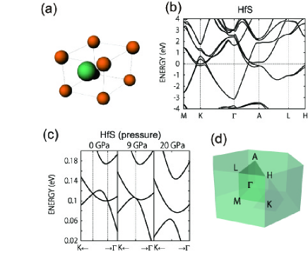
Examples of NLSs can be found by the argument in Sect. 2.3. One can start with a narrow-gap semiconductor and close the gap on a mirror/glide plane, and one can obtain an NLS when the mirror/glide eigenvalues are different between the two bands involved. For example, we find that HfS has nodal lines near the Fermi level. The structure of HfS is shown in Fig. 7(a), which has the space group No.187 (). Figure 7(b) shows the electronic band structure of HfS. If the SOC is neglected, Dirac nodal lines exist around the K points on the plane. The SOC lifts the degeneracy of the Dirac nodal lines, and Weyl nodal lines appear instead near the K points on the mirror plane . By applying pressure (Fig. 7(c)) or by atomic substitution from S to Se, the nodal lines become smaller. At 9 GPa, the nodal lines shrink to points, and then a gap opens above 9 GPa.
4.2 Nodal lines stemming from the Berry phase
The second mechanism (B) occurs in spinless systems with inversion and TR symmetries. Spinless systems include electronic systems with zero SOC and bosonic systems such as magnonic and photonic systems. Examples of electronic systems include calcium at high pressure [72] and AX2 (A = Ca, Sr, Ba; X = Si, Ge, Sn) [74]. The Berry phase around the nodal line is , and this Berry phase topologically protects the nodal line. In spinless systems with inversion and TR symmetries, the Berry phase along any closed loop is quantized as an integer multiple of , as shown in the following. Here, the Berry phase along a loop is defined as
| (3) |
where the sum is over the occupied states and the system is assumed to have a gap everywhere along loop . The Berry phase is defined modulo , corresponding to a gauge degree of freedom. Under the product of TR and spatial inversion operations, this quantity is transformed into , and therefore we obtain , i.e., for any loop . The Berry phase around a nodal line from this mechanism (B) is (Fig. 8(b)), and therefore the nodal line is protected because of the quantization of the Berry phase.
Because of the topological character of these nodal lines, new topological invariants () can be introduced to identify NLSs [17]. The invariants are
| (4) | |||
| (5) |
where is the parity eigenvalue of the th occupied band at one of the TRIM . are primitive reciprocal lattice vectors. When , the system is guaranteed to be in the NLS phase. When the SOC is taken into account, the invariants coincide with Fu–Kane–Mele invariants [54, 17]. In fact, the SOC changes an NLS into an insulator or a Dirac semimetal, which has corresponding Fu–Kane–Mele invariants. [17, 75]
To intuitively understand the appearance of a nodal line in a spinless system with TR and inversion symmetries, it is useful to consider the following effective model. An effective model for a single valence band and a single conduction band with these symmetries is generally expressed as
| (6) |
where a term is prohibited by these symmetries. Its band gap closes only if the two conditions and are satisfied simultaneously. Their solutions give a nodal line in space, and the Berry phase around the nodal line turns out to be , in agreement with the discussion in the previous paragraph.
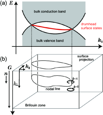
In many NLSs, characteristic surface states called drumhead surface states appear. In the surface Brillouin zone, they appear in a region surrounded by the projection of the nodal line (Fig. 8(a)). While the appearance of drumhead surface states can be seen from a calculation based on an effective model [17], they do not necessarily appear in every NLS [72].
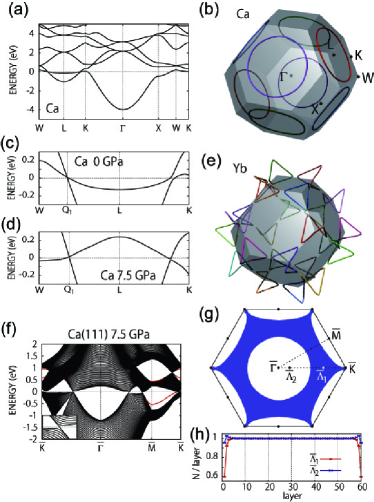
Nodal lines from this mechanism can be seen in alkaline-earth metals Ca, Sr, and in Yb when the SOC is neglected, from ab initio calculation. In reality, the SOC gives a small gap along the otherwise gapless nodal lines. Ca, Sr, and Yb are nonmagnetic metals, having a face-centered cubic (fcc) lattice, with the space group Fmm (No.225). Let denote the lattice parameter. Figure 9(a) shows the electronic structure of Ca obtained by local density approximation (LDA). The top of the valence band, which is relatively flat near the L points, originates from the orbital oriented along the [111] axis having strong bonding, while most of the other valence bands originate from the and orbitals. Around the L points, their crossing yields four nodal lines around the L points within approximately 0.01 eV near the Fermi level, as shown in Fig. 9(a). The four nodal lines (Fig. 9(b)) are slightly away from the faces of the first Brillouin zone, except along the - lines (Q1 in Fig. 9(c)) by symmetry. The Berry phase around each nodal line is numerically confirmed to be . At ambient pressure, Ca is not an NLS, because the two bands forming the nodal lines both disperse downward around the L points (Fig. 9(c)). Ca becomes an NLS under pressure, as shown in the band structure at 7.5 GPa in Fig. 9(d). The nodal lines in Yb with the neglected SOC are shown in Fig. 9(e). These nodal lines can be understood from those in Ca via a Lifshitz transition of nodal lines. Figure 9(f) shows the electronic structure of the Ca(111) surface at 7.5 GPa. Drumhead surface states connecting the gapless points exist near the Fermi level around the point, which are isolated from the bulk states.
4.3 Surface charges and nodal lines with the Berry phase
This Berry phase is closely related to the Zak phase, as we explain here. We calculate the Zak phase along a certain reciprocal vector . For the calculation, we decompose the wavevector into the components along and perpendicular to : , . For each value of , one can define the Zak phase by
| (7) |
where is the bulk eigenstate in the th band and the sum is over the occupied states. Here, the gauge is taken as . The Zak phase is defined in terms of modulo . We focus on the cases without the SOC and neglect the spin degeneracy. Under both inversion and TR symmetries, the Zak phase takes a quantized value of 0 or [20, 76]. The Zak phase is related to the charge polarization at surface momentum for a surface perpendicular to [77, 78]. Additionally, in a 3D system, if the system at each is regarded as a 1D system, then the product of the Zak phase and is equal to modulo , where is the surface charge when the system at a given is regarded as a 1D system. For an insulator, the surface polarization charge density at a given surface is given by [77].
Because the Berry phase around the nodal line is , the Zak phase jumps by as changes across the nodal line. For example, for the Ca (111) surface, the region of the Zak phase is shown as the shaded region in Fig. 9(g), and this region is surrounded by the projections of the nodal lines. For example, because the Zak phases for points and in Fig. 9(h) are and , respectively, the surface polarization charges are and (mod ). This difference in surface polarization charges can be directly seen in the charge distribution for the slab geometry. At the charge distribution is almost constant, whereas at it decreases by near each surface. Thus, the surface polarization charge from the Zak phase is attributed to bulk states, not to surface states [39].
The area of the region with in Fig. 9(g) is of the area of the Brillouin zone, and the total surface polarization charge density is per surface unit cell. A nonzero surface polarization charge does not violate the inversion symmetry because the two surfaces of the slab have the same surface polarization charges. Nevertheless, in reality this amount of surface charge does not appear since the correspondence between the surface charge and the Zak phase is correct only for insulators. In reality, the excess surface charge is screened by free carriers because the system is a semimetal, and this results in surface dipoles at the surface. From the above argument, carriers in the semimetal screen the surface charge within a screening length on the order of nanometers.
4.4 Transitions from nodal-line semimetals to other topological phases
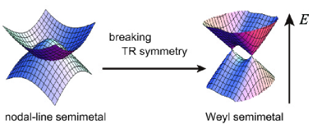
Thus far, we discussed NLSs with the Berry phase. Because this NLS phase requires both TR and inversion symmetries, breaking of either TR or inversion symmetry leads to transitions into other phases including topological semimetal phases. As an example, let us consider a nodal line encircling one of the TRIM, such as one of those in Ca (Fig. 9(b)). By breaking TR symmetry, such an NLS always becomes a spinless WSM [79], which can be easily seen in terms of an effective model. The nodal line is formed by the conduction and valence bands with opposite parity eigenvalues at the TRIM. [79] Therefore, the parity operator is given by , and the nodal line can be described by the effective Hamiltonian
| (8) |
where is the wavevector measured from the TRIM. The nodal line is described as . A TR-breaking term is then represented by , with being an odd function of owing to inversion symmetry. Since the nodal line encloses the TRIM () by assumption, wavevectors satisfying always exist somewhere on the nodal line, and Weyl nodes necessarily emerge on it. As a result, when a nodal line encloses one of the TRIM, the NLS undergoes a transition to a spinless WSM by breaking TR symmetry [79], as schematically shown in Fig. 10. It is theoretically predicted that this kind of phase transition is driven by circularly polarized light in electronic systems. [80, 81, 82, 83, 84, 85]. Meanwhile, when nodal lines do not enclose one of the TRIM, the TR breaking does not necessarily lead to topological semimetals, but it may lead either to an insulator or to a Weyl semimetal. Similarly, by breaking the inversion symmetry, the NLS either remains an NLS or becomes an insulator or a Weyl semimetal, depending on crystallographic symmetries [79]. Thus, by starting with one topological semimetal material, one can obtain other topological phases by breaking symmetries, and such topological phase transitions stem from the interplay between topology and symmetry. Understanding of this interplay will give further insight in ab initio studies of topological semimetal materials.
5 Numerical Tools for Characterizing Topological Semimetal Materials
In this section, for readers’ convenience we briefly summarize the numerical methods used in this review.
5.1 Self-energy correction
In general, the band gap estimated in the density functional theory (DFT) with the LDA is smaller than its real value. Therefore, the LDA tends to predict nontrivial phases in narrow- and pseudogap systems even when they are in the trivial phases. Thus, high precision in ab initio calculations is required to search for nontrivial topological phases of matter. One of the suitable approaches beyond the LDA is the Green’s function method for self-energy correction. Within the Green’s function method, the GW method is the most widely used approximation for the self-energy [86]. The band structure in the GW approximation (GWA) is obtained by diagonalizing the following GW Hamiltonian:
| (9) |
where , , and are the Kohn-Sham Hamiltonian in the LDA, the LDA exchange-correlation potential, and the self-energy in the GWA, respectively. is obtained from the convolution integral between the Green’s function in the LDA and the screened interaction . For example, within the LDA, tellurium (Te) is incorrectly described as a metal in the LDA, and the GW method correctly reproduces the existence of the band gap.
5.2 Wannier function
In discussing the topology of electronic structures, it is useful to derive an ab initio low-energy effective model describing the bands near the Fermi level. The transfer integral in the low-energy effective model is given by
| (10) |
where is the maximally localized Wannier function (MLWF) of the th orbital localized at the unit cell in the space spanned by the states near the Fermi energy [87, 88]. The MLWF is defined from the associated Bloch function
| (11) |
where is the Fourier transform of and the coefficients are determined such that the quadratic extent of the wave function
| (12) |
is minimized. The position operator in Eq. (12) is treated in terms of the Berry connection in space.
5.3 Monopole charge
In the search for Weyl semimetals using ab initio calculations, it is sometimes difficult to see whether there is a Weyl node or not because it is numerically difficult to distinguish between the case with no gap and that with a tiny gap. This problem is solved by numerically calculating the value of the monopole charge at the point considered. By extending the numerical scheme for the calculation of the Chern number [89], we can calculate the monopole charge by the following scheme.
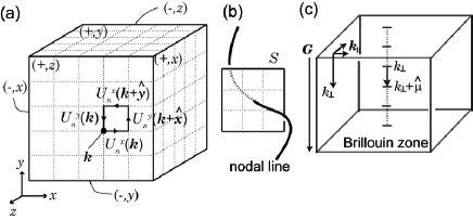
We first define a small cubic region around the point, as shown in Fig. 11(a), and calculate the integral of the Berry curvature over the surfaces of this region. To this end, the faces of this cubic region are divided into small square meshes. For each edge of the small square meshes, we define a link variable for the th band as
| (13) |
where is the direction of the edge and is the vector along the edge between the nearest mesh points along the direction. We label the six faces of the cubic region as according to the orientations of their normal vectors out of the cube, where and . The monopole charge in the cube is calculated from as
| (14) | ||||
| (15) |
where is a mesh point on the face specified by , so that the square meshes with vertices (, , , ) cover the face. is the lattice field strength in the square mesh (, , , ) on the faces of the cube:
| (16) | ||||
| (17) |
is the difference in the gauge potential between the neighboring mesh points displaced by :
| (18) | ||||
| (19) |
The numerical convergence of this method with increasing the number of meshes is very rapid. Several tens of mesh points per each direction is usually sufficient to obtain a correct result.
5.4 Berry phase
The nodal line discussed in Sect. 4.2 is characterized by the Berry phase around the nodal line. Here we explain the numerical method used to calculate this Berry phase around the nodal line. We consider a square encircling the nodal line, and we divide the square into meshes (Fig. 11(b)). For notational simplicity, we set the edges of the square to be along the and axes. The Berry phase for the th band along the square is defined as
| (20) |
where and are the lattice field strength and the difference in the gauge potential for the meshes in the square , and the summation is taken so that the meshes cover the whole square. In spinless systems with TR and inversion symmetries, the Berry phase is quantized to be either or (mod ), and if it is , it is indeed the nodal line discussed in Sect. 4.2.
5.5 Zak phase
The Zak phase for is calculated as [90, 77, 78]
| (21) |
where and in the determinant run over the occupied bands. is the vector between the nearest mesh points along the reciprocal lattice vector , and the product is taken over the wavevector such that the path covers the reciprocal lattice vector , as shown in Fig. 11(c). Note that in calculating the Zak phase, the gauge should be chosen to satisfy . This gauge choice is related to the choice of the unit cell, and it affects the value of the Zak phase and the polarization [77].
6 Summary
We have seen various types of topological semimetals, which have degeneracies between bands, apart from those originating from symmetry. After brief reviews of basic properties of topological semimetals, we explained how these properties are used for the search for topological semimetals using ab initio calculations. For example, we showed that LuSI at high pressure and Te at high pressure are Weyl semimetals, and that Ca under pressure and HfS are nodal-line semimetals. We also explained that various topological metals are related to each other in a complex way. This shows a profound interplay between topology and symmetry in the band theory of solids. Thus, the studies on TIs and topological metals have provided us with renewed interest in the band theory of solids.
Through close collaborations among theories, experiments, and ab initio calculations, we have been obtaining new insights into the electronic properties of solids.
Acknowledgements.
We thank Takashi Miyake for fruitful discussions and Shoji Ishibashi for providing us with the ab initio code (QMAS) and pseudopotentials. This work was supported by Grants-in-Aid for Scientific Research (Nos.26287062, 26600012); by the Computational Materials Science Initiative (CMSI), Japan; by CREST, JST (Grant No. JPMJCR14F1); by JSPS KAKENHI Grant Number 16J08552; and also by MEXT Elements Strategy Initiative to Form Core Research Center (TIES).References
- [1] C. L. Kane and E. J. Mele, Phys. Rev. Lett. 95, 146802 (2005).
- [2] C. L. Kane and E. J. Mele, Phys. Rev. Lett. 95, 226801 (2005).
- [3] B. A. Bernevig and S.-C. Zhang, Phys. Rev. Lett. 96, 106802 (2006).
- [4] M. Z. Hasan and C. L. Kane, Rev. Mod. Phys. 82, 3045 (2010).
- [5] X. L. Qi and S. C. Zhang, Rev. Mod. Phys. 83, 1057 (2011).
- [6] B. Yan and S.-C. Zhang, Rep. Prog. Phys. 75, 096501 (2012).
- [7] K. von Klitzing, G. Dorda, and M. Pepper, Phys. Rev. Lett. 45, 494 (1980).
- [8] L. Fu, Phys. Rev. Lett. 106, 106802 (2011).
- [9] S. Murakami, New J. Phys. 9, 356 (2007).
- [10] X. Wan, A. M. Turner, A. Vishwanath, and S. Y. Savrasov, Phys. Rev. B 83, 205101 (2011).
- [11] Z. Wang, H. Weng, Q. Wu, X. Dai, and Z. Fang, Phys. Rev. B 88, 125427 (2013).
- [12] Z. Wang, S. Yan, X.-Q. Chen, C. Franchini, G. Xu, H. Weng, X. Dai, and Z. Fang, Phys. Rev. B 85, 195320 (2012).
- [13] K. Mullen, B. Uchoa, and D. T. Glatzhofer, Phys. Rev. Lett. 115, 026403 (2015).
- [14] C. Fang, Y. Chen, H.-Y. Kee, and L. Fu, Phys. Rev. B 92, 081201 (2015).
- [15] Y. Chen, Y. Xie, S. A. Yang, H. Pan, F. Zhang, M. L. Cohen, and S. Zhang, Nano Lett. 15, 6974 (2015).
- [16] H. Weng, Y. Liang, Q. Xu, R. Yu, Z. Fang, X. Dai, and Y. Kawazoe, Phys. Rev. B 92, 045108 (2015).
- [17] Y. Kim, B. J. Wieder, C. L. Kane, and A. M. Rappe, Phys. Rev. Lett. 115, 036806 (2015).
- [18] R. Yu, H. Weng, Z. Fang, X. Dai, and X. Hu, Phys. Rev. Lett. 115, 036807 (2015).
- [19] L. S. Xie, L. M. Schoop, E. M. Seibel, Q. D. Gibson, W. Xie, and R. J. Cava, APL Mater. 3, 083602 (2015).
- [20] Y.-H. Chan, C.-K. Chiu, M. Chou, and A. P. Schnyder, Phys. Rev. B 93, 205132 (2016).
- [21] M. Zeng, C. Fang, G. Chang, Y.-A. Chen, T. Hsieh, A. Bansil, H. Lin, and L. Fu, arXiv:1504.03492 (2015).
- [22] A. Yamakage, Y. Yamakawa, Y. Tanaka, and Y. Okamoto, J. Phys. Soc. Jpn. 85, 013708 (2016).
- [23] J. Zhao, R. Yu, H. Weng, and Z. Fang, Phys. Rev. B 94, 195104 (2016).
- [24] K.-Y. Yang, Y.-M. Lu, and Y. Ran, Phys. Rev. B 84, 075129 (2011).
- [25] W. Witczak-Krempa and Y.-B. Kim, Phys. Rev. B 85, 045124 (2012).
- [26] X. Wan, A. M. Turner, A. Vishwanath, and S. Y. Savrasov, Phys. Rev. B 83, 205101 (2011).
- [27] F. R. Klinkhamer and G. E. Volovik, Int. J. Mod. Phys. A 20, 2795 (2005).
- [28] J.-H. Jiang, Phys. Rev. A 85, 033640 (2012).
- [29] M. V. Berry, Proc. R. Soc. London, Ser. A 392, 45 (1984).
- [30] G. E. Volovik, The Universe in a Helium Droplet (Oxford University Press, Oxford, 2009).
- [31] T. Ojanen, Phys. Rev. B 87, 245112 (2013).
- [32] R. Okugawa and S. Murakami, Phys. Rev. B 89, 235315 (2014).
- [33] F. D. M. Haldane, arXiv:1401.0529 (2014).
- [34] G. Xu, H. Weng, Z. Wang, X. Dai, and Z. Fang, Phys. Rev. Lett. 107, 186806 (2011).
- [35] Z. Wang, M. G. Verniory, S. Kushwaha, M. Hirschberger, E. V. Chulkov, A. Ernst, N. P. Ong, R. J. Cava, and B. A. Bervervig, Phys. Rev. Lett 117, 236401 (2016).
- [36] A. A. Burkov and L. Balents, Phys. Rev. Lett. 107, 127205 (2011).
- [37] A. A. Burkov, M. D. Hook, and L. Balents, Phys. Rev. B 84, 235126 (2011).
- [38] J. Liu and S. Vanderbilt, Phys. Rev. B 90, 155316 (2014).
- [39] M. Hirayama, R. Okugawa, S. Ishibashi, S. Murakami, and T. Miyake, Phys. Rev. Lett. 114, 206401 (2015).
- [40] Y. Sun, S.-C. Wu, M. N. Ali, C. Felser, and B. Yan, Phys. Rev. B 92, 161107 (2015).
- [41] H. Weng, C. Fang, Z. Fang, B. A. Bernevig, and X. Dai, Phys. Rev. X 5, 011029 (2015).
- [42] S.-M. Huang, S.-Y. Xu, I. Belopolski, C.-C. Lee, G. Chang, B. Wang, N. Alidoust, M. Neupane, H. Zheng, D. Sanchez, A. Bansil, G. Bian, H. Lin, and M. Z. Hasan, Proc. Natl. Acad. Sci. U.S.A. 113, 1180 (2016).
- [43] A. A. Soluyanov, D. Gresch, Z. Wang, Q. Wu, M. Troyer, X. Dai, and A. B. Bernevig, Nature 527, 495 (2015).
- [44] T. Rauch, S. Achilles, J. Henk, and I. Mertig, Phys. Rev. Lett. 114, 236805 (2015).
- [45] G. B. Halász and L. Balents, Phys. Rev. B 85, 035103 (2012).
- [46] S.-M. Huang, S.-Y. Xu, I. Belopolski, C.-C. Lee, G. Chang, B. Wang, N. Alidoust, G. Bian, M. Neupane, C. Zhang, S. Jia, A. Bansil, H. Lin, and M. Z. Hasan, Nat. Commun. 6, 7373 (2015).
- [47] S. Y. Xu, N. Alidoust, I. Belopolski, Z. Yuan, G. Bian, T. R. Chang, H. Zheng, V. N. Strocov, D. S. Sanchez, G. Chang, C. Zhang, D. Mou, Y. Wu, L. Huang, C. C. Lee, S. M. Huang, B. Wang, A. Bansil, H. T.. Jeng, T. Neupert, A. Kaminski, H. Lin, S. Jia, and M. Z. Hasan , Nat. Phys. 11, 748 (2015).
- [48] L. X. Yang, Z. K. Liu, Y. Sun, H. Peng, H. F. Yang, T. Zhang, B. Zhou, Y. Zhang, Y. F. Guo, M. Rahn, D. Prabhakaran, Z. Hussain, S.-K. Mo, C. Felser, B. Yan, and L. Chen, Nat. Phys. 11, 728 (2015).
- [49] S.-Y. Xu, I. Belopolski, N. Alidoust, M. Neupane, G. Bian, C. Zhang, R. Sankar, G. Chang, Z. Yuan, C.-C. Lee, S.-M. Huang, H. Zheng, J. Ma, D. S. Sanchez, B. Wang, A. Bansil, F. Chou, P. P. Shibayev, H. Lin, S. Jia, and M. Z. Hasan, Science 349, 613 (2015).
- [50] B. Q. Lv, H. M. Weng, B. B. Fu, X. P. Wang, H. Miao, J. Ma, P. Richard, X. C. Huang, L. X. Zhao, G. F. Chen, Z. Fang, X. Dai, T. Qian, and H. Ding, Phys. Rev. X 5, 031013 (2015).
- [51] B. Q. Lv, N. Xu, H. M. Weng, J. Z. Ma, P. Richard, X. C. Huang, L. X. Zhao, G. F. Chen, C. E. Matt, F. Bisti, V. N. Strocov, J. Mesot, Z. Fang, X. Dai, T. Qian, M. Shi, and H. Ding, Nat. Phys. 11, 724 (2015).
- [52] T. L. Hughes, E. Prodan, and B. A. Bernevig, Phys. Rev. Lett. 83, 245132 (2011).
- [53] A. M. Turner, Y. Zhang, R. S. K. Mong, and A. Vishwanath, Phys. Rev. B 85, 165120 (2012).
- [54] L. Fu, C. L. Kane, and E. J. Mele, Phys. Rev. Lett. 98, 106803 (2007).
- [55] S. Murakami and S. Kuga, Phys. Rev. B 78, 165313 (2008).
- [56] S.-Y. Xu, Y. Xia, L. A. Wray, S. Jia, F. Meier, J. H. Dil, J. Osterwalder, B. Slomski, A. Bansil, H. Lin, R. J. Cava, and M. Z. Hasan, Science 332, 560 (2011).
- [57] T. Sato, K. Segawa, K. Kosaka, S. Souma, K. Nakayama, K. Eto, T. Minami, Y. Ando, and T. Takahashi, Nat. Phys. 7, 840 (2011).
- [58] S. Murakami, M. Hirayama, R. Okugawa, and T. Miyake, Sci. Adv. 3, e1602680 (2017).
- [59] K. Ishizaka, M. S. Bahramy, H. Murakawa, M. Sakano, T. Shimojima, T. Sonobe, K. Koizumi, S. Shin, H. Miyahara, A. Kimura, K. Miyamoto, T. Okuda, H. Namatame, M. Taniguchi, R. Arita, N. Nagaosa, K. Kobayashi, Y. Murakami, R. Kumai, Y. Kaneko, Y. Onose, and Y. Tokura, Nat. Mater. 10, 521 (2011).
- [60] B.-J. Yang, M. S. Bahramy, R. Arita, H. Isobe, E.-G. Moon, and N. Nagaosa, Phys. Rev. Lett. 110, 086402 (2013).
- [61] M. S. Bahramy, B.-J. Yang, R. Arita, and N. Nagaosa, Nat. Commun. 3, 679 (2012).
- [62] C. J. Bradley and A. P. Cracknell, The Mathematical Theory of Symmetry in Solids: Representation Theory for Point Groups and Space Groups (Oxford Univ Press, Oxford, 2010).
- [63] V. B. Anzin, M. I. Eremets, Yu. V. Hosichkin, A. I. Nadezhdinskii, and A. M. Shirokov, Phys. Status Solidi (a) 42, 385 (1977).
- [64] S. Tutihasi and I. Chen, Phys. Rev. 158, 623 (1967).
- [65] T. Doi, K. Nakao, and H. Kamimura, J. Phys. Soc. Jpn. 28, 36 (1970).
- [66] S. M. Young, S. Zaheer, J. C. Y. Teo, C. L. Kane, E. J. Mele, and A. M. Rappe, Phys. Rev. Lett. 108, 140405 (2012).
- [67] Z. K. Liu, B. Zhou, Y. Zhang, Z. J. Wang, H. M. Weng, D. Prabhakaran, S.-K. Mo, Z. X. Shen, Z. Fang, X. Dai, Z. Hussain, and Y. L. Chen, Science 343, 864 (2014).
- [68] S. Y. Xu, C. Liu, S. K. Kushwaha, R. Sankar, J. W. Krizan, I. Belopolski, M. Neupane, G. Bian, N. Alidoust, T. R. Chang, H. T. Jeng, C. Y. Huang, W. F. Tsai, H. Lin, P. P. Shibayev, F. C. Chou, R. J. Cava, and M. Z. Hasan, Science 347, 294 (2015).
- [69] M. Neupane, S.-Y. Xu, R. Sankar, N. Alidoust, G. Bian, C. Liu, I. Belopolski, T.-R. Chang, H.-T. Jeng, H. Lin, A. Bansil, F. Chou, and M. Z. Hasan, Nat. Commun. 5, 3786 (2014).
- [70] S. Borisenko, Q. Gibson, D. Evtushinsky, V. Zabolotnyy, B. Büchner, and R. J. Cava, Phys. Rev. Lett. 113, 027603 (2014).
- [71] B.-J. Yang and N. Nagaosa, Nat. Commun. 5, 4898 (2014).
- [72] M. Hirayama, R. Okugawa, T. Miyake, and S. Murakami, Nat. Commun. 8, 14022 (2017).
- [73] G. Bian, T.-R. Chang, H. Zheng, S. Velury, S.-Y. Xu, T. Neupert, C.-K. Chiu, S.-M. Huang, D. S. Sanchez, I. Belopolski, N. Alidoust, P.-J. Chen, G. Chang, A. Bansil, H.-T. Jeng, H. Lin, and M. Z. Hasan, Phys. Rev. B 93, 121113(R) (2016).
- [74] H. Huang, J. Liu, D. Vanderbilt, and W. Duan, Phys. Rev. B 93, 201114(R) (2016).
- [75] S. Kobayashi, Y. Yamakawa, A. Yamakage, T. Inohara, Y. Okamoto, and Y. Tanaka, Phys. Rev. B 95, 245208 (2017).
- [76] T. Kariyado and Y. Hatsugai, Phys. Rev. B 88, 245126 (2013).
- [77] D. Vanderbilt and R. D. King-Smith, Phys. Rev. B 48, 4442 (1993).
- [78] R. Resta, Rev. Mod. Phys. 66, 899 (1994).
- [79] R. Okugawa and S. Murakami, Phys. Rev. B 96, 115201 (2017).
- [80] A. Narayan, Phys. Rev. B 94, 041409 (2016).
- [81] Z. Yan and Z. Wang, Phys. Rev. Lett. 117, 087402 (2016).
- [82] C.-K. Chan, Y.-T. Oh, J. H. Han, and P. A. Lee, Phys. Rev. B 94, 155206 (2016).
- [83] K. Taguchi, D. -H. Xu, A. Yamakage, and K. T. Law, Phys. Rev. B 94, 155206 (2016).
- [84] M. Ezawa, Phys. Rev. B 96, 041205(R) (2017) (2017).
- [85] Z. Yan and Z. Wang, Phys. Rev. B 96, 041206(R) (2017) (2017).
- [86] L. Hedin, Phys. Rev. 139, A796 (1965); L. Hedin and S. Lundqvist, Solid State Physics, ed. H. Ehrenreich, F. Seitz, and D. Turnbull (Academic, New York, 1969) Vol. 23.
- [87] N. Marzari and D. Vanderbilt, Phys. Rev. B 56, 12847 (1997).
- [88] I. Souza, N. Marzari, and D. Vanderbilt, Phys. Rev. B 65, 035109 (2001).
- [89] T. Fukui, Y. Hatsugai, and H. Suzuki, J. Phys. Soc. Jpn. 74, 1674 (2005).
- [90] R. D. King-Smith and D. Vanderbilt, Phys. Rev. B 47, 1651 (1993).