Fundamental Band Gap and Alignment of Two-Dimensional Semiconductors Explored by Machine Learning
Abstract
Two-dimensional (2D) semiconductors isoelectronic to phosphorene has been drawing much attention recently due to their promising applications for next-generation (opt)electronics. This family of 2D materials contains more than 400 members, including (a) elemental group-V materials, (b) binary III-VII and IV-VI compounds, (c) ternary III-VI-VII and IV-V-VII compounds, making materials design with targeted functionality unprecedentedly rich and extremely challenging. To shed light on rational functionality design with this family of materials, we systemically explore their fundamental band gaps and alignments using hybrid density functional theory (DFT) in combination with machine learning. First, GGA-PBE and HSE calculations are performed as a reference. We find this family of materials share similar crystalline structures, but possess largely distributed band-gap values ranging approximately from 0 to 8 eV. Then, we apply machine learning methods, including Linear Regression (LR), Random Forest Regression (RFR), and Support Vector Machine Regression (SVR), to build models for prediction of electronic properties. Among these models, SVR is found to have the best performance, yielding the root mean square error (RMSE) less than 0.15 eV for predicted band gaps, VBMs, and CBMs when both PBE results and elemental information are used as features. Thus, we demonstrate machine learning models are universally suitable for screening 2D isoelectronic systems with targeted functionality, and especially valuable for the design of alloys and heterogeneous systems.
I Introduction
Last decade has witnessed the rocketing development of two-dimensional (2D) materials, which find promising applications in next-generation electronics and optoelectronics Novoselov et al. (2004); Zhang et al. (2005); Mak and Shan (2016); Fiori et al. (2014). The performance of a 2D electronic device depends sensitively on fundamental electronic properties of the candidate material: a non-zero band gap, proper band edge positions, and high mobility are in general the requisites. In contrary to semi-metallic graphene Novoselov et al. (2004); Zhang et al. (2005) and low-mobility transition metal dichalcogenides (TMDs) Radisavljevic et al. (2011); Perera et al. (2013) that fail to deliver good device performance, phosphorene is semiconducting while still maintaining a high hole mobility Li et al. (2014); Liu et al. (2014); Koenig et al. (2014); Rodin et al. (2014); Ling et al. (2015), thereby emerging as a potential candidate for 2D electronics. However, poor chemical stability has limited phosphorene for practical applications Liu et al. (2015). To overcome such obstacles, searching for 2D materials with similar electronic properties but better chemical stability is essential.
Recently, high-throughput materials screening has emerged as an effective method to search for materials with targeted functionality Curtarolo et al. (2013); De Jong et al. (2015); Setyawan and Curtarolo (2010); Hautier et al. (2011). The workflow for materials discovery is separated to different layers: starting with crude and low-precision computations to narrow the candidacy pool, and followed by precise but expensive calculations to identify the candidate materials. The initial materials pool is usually a subset of the ICSD database ICS with large amount of candidates, resulting in tedious prescreening and large computational efforts. A prescreening method that is both accurate and computationally efficient is greatly desired, where machine learning can play an important role. In combination with density functional theory (DFT), machine learning has demonstrated valuable applications in functional materials design Ward and Wolverton (2017), properties predictions Ward et al. (2016); Deml et al. (2016); Pilania et al. (2017); Lee et al. (2016), and many other fields Ramprasad et al. (2017); Balachandran et al. (2015) for traditional bulk materials. It is intriguing to apply such machine learning methods to two-dimensional systems to accelerate materials discovery, which is largely unexplored but fundamentally and technologically important.
Here, we have explored the fundamental band gaps and band alignments of a group of 2D semiconductors that are isoelectronic to phosphorene using machine learning techniques in combination with density functional theory. The methodology is discussed in Sec. II, including details of density functional calculations (Sec. II.1) and a brief introduction of machine learning models (Sec. II.2). We describe the isoelectronic materials design method in Sec. II.3. Following this method, more than 400 materials are constructed and calculated, including (a) elemental group-V materials, (b) binary III-VII and IV-VI compounds, (c) ternary III-VI-VII and IV-V-VII compounds. Among this family of materials, many have been successfully synthesized Ji et al. (2016); Zhang et al. (2016) and found special applications in different research fields Haleoot et al. (2017); Fei et al. (2016). The richness in electronic properties of these materials is categorized and analyzed in Sec. III. Next, in Sec. IV, we apply machine learning methods, including Linear Regression (LR), Random Forest Regression (RFR), and Support Vector Machine Regression (SVR), to predict electronic properties for this family of 2D materials. Then we summarize our key findings in Sec. V.
II Methodology
II.1 Computational Details for Density Functional Methods
All our calculations are based on DFT using projector-augmented waves Blöchl (1994) (PAW) as implemented in the VASP Kresse and Furthmüller (1996) code. We have used periodic boundary conditions throughout the study, with monolayer structures represented by a periodic array of slabs separated by a vacuum region at least 15 Å thick. We used the Perdew-Burke-Ernzerhof (PBE) Perdew et al. (1996) exchange-correlation functional for initial structure optimization based on the conjugate gradient method Hestenes and Stiefel (1952) with a 400 eV energy cutoff. All geometries are treated as optimized when none of the residual Hellmann-Feynman forces exceeded eV/Å. On top of PBE-optimized structures, a single-shot screened hybrid functional calculation (HSE) Heyd et al. (2003, 2006) is performed to obtain fundamental band gaps and band alignments of the material. We have used standard values for the mixing parameter (0.25) and the range-separation parameter (0.2 Å-1). The reciprocal space was sampled by a grid Monkhorst and Pack (1976) finer than -points in the Brillouin zone of the primitive unit cell.
II.2 Machine Learning Methods
The obtained DFT results are then analyzed with machine learning models as implemented in scikit-learn skl package. Relation between target electronic properties and predictors can be established via supervised learning methods. A good predictive model depends sensitively on choice of regression models, selection of predictors, as well as the quality of our dataset. For a given data set, it is important to select proper predictors and suitable regression models to achieve good predictive ability with high accuracy. To achieve this goal in current study, we have selected three different predictor sets, which are different combinations of computed PBE results and fundamental signatures of constituent elements. Then, we utilize a variety of regression methods, including Linear Regressions, Random Forest Regression, and Support Vector Machine Regression, to predict target electronic properties.
In the LR method, the regression coefficients of predictors, , are determined by optimizing the following cost function : . In addition, other LR methods with regularizations, LASSO and Ridge are also used in this study. On top of the ordinary least square linear regression method, LASSO include an additional penalty term in the cost function, while Ridge regression method add a regularization term . These penalty terms can effectively mitigate the overfitting problem especially when the predictor sets are large.
When the relation between the target property and the predictors is not linear, regression methods like RFR and SVR with a non-linear kernel are supposed to capture the nonlinear feature-target relationship. Random Forest is one type of ensemble methods. It grows a number of decision trees via bootstrapping the sample space. For each decision tree, a randomly selected subset of the feature space is used, which can effectively minimize the correlation between different trees. Then, the target value is predicted by majority vote of these trees for classification or averaging the predicted result of each tree in regression problems. Importantly, the Random Forest model is easy to interpret and It can output the relative importance of different features, thereby providing insights on the elemental signatures that determines targeted electronic properties of materials in present study.
We also use a SVR model with a Radial Basis Function (RBF) kernel to predict calculated electronic properties with fundamental materials features. The Support Vector Machine model utilizes the kernel trick to map low-dimensional non-separable data to a higher dimension where they can be separated via a hyper-plane. The optimized hyper-plane can be identified by so-called supported vectors. The kernel trick makes it possible to compute the inner product of the projected data in the higher dimension without specifying the mapping function, which is usually time-consuming or even impossible to specify. SVR uses a hinge-loss function , which is minimized during the model training process. The RBF kernel used in present work has the form of .
| Target property | Predictors Set I | Predictors Set II | Predictors Set III |
|---|---|---|---|
| Elements Signatures | , Elements Signatures | ||
| Elements Signatures | , Elements Signatures | ||
| Elements Signatures | , Elements Signatures |
In addition to the type of machine learning methods we choose, a proper selection of feature space is also critical to achieve robust and accurate prediction. Previous studies usually include a large amount of predictors in the feature space and then conduct dimension reduction, which is likely to hide important physical insights of the model. Here, instead, we intend to compare the prediction power of PBE results as features and merely fundamental chemical and physical signatures of constituent elements in the materials. With this consideration, we have built three different sets of predictors: In Set-I, PBE results, band gap, VBM, and CBM, are the only feature used to predict related HSE values; In Set-II, we include only elemental signatures for each material, such as atomic mass, ionization energy, electron affinity, electronegativity, as well as electronegativity difference between cations and anions; Set-III is a combination of Set-I and Set-II. Features in Set-I depend on less time-consuming PBE calculations, while Set-II is more convenient to obtain with no requirement of any DFT calculations.
II.3 Isoelectronic Materials Design
2D group-V elemental materials, such as phosphorene Liu et al. (2014); Zhu and Tománek (2014) and antimonene Zhang et al. (2015), can be stabilized in two distinct structural phases as shown in Fig. 1(a) and (b). In both structural phases, each atom forms three covalent bonds of type with adjacent atoms, as well as lone-pair electrons, which fulfils the octet rule. The pyramid formed by a center atom and its three nearest neighbors can be arranged in a variety of ways, thereby leading to a rich design space for structural polymorphs Guan* et al. (2014).
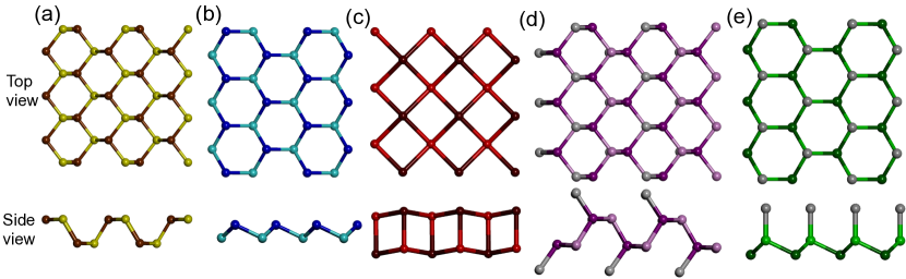
Binary compounds can be derived from their elemental counterparts by cation mutation while the averaged valence electrons are conserved to be five Zhu et al. (2015). Based on such a principle, group IV-VI and III-VII compounds can be conveniently designed and they are isoelectronic to the well-studied group-V elemental materials. In addition to two base structures mentioned previously, III-VII compounds can also be stabilized in a special structure with a primitive cell of approximately square shape, as shown in Fig. 1(c). In fact, for Indium Iodide, an existing compound of the III-VII family, Phase-III is the most energetically favored structure among the polymorphs mentioned here Wang et al. (2017). Thus, we also include this structural phase as one of the base structure for 2D materials design in present study.
The isoelectronic design principle can be further generalized to construct ternary compounds. As shown in Fig. 1(d) and (e), III-VI-VII and IV-V-VII compounds share similar structures as elemental and binary materials discussed above; indeed, they are isoelectronic. Taking phosphorene of Phase-II as the starting material, we change half of P atoms to a group IV element, such as Si. bonding in the material is maintained and P atoms still have the close-shell electron configuration. However, as Si has one less valence electron, one unpaired electron exists for Si rather than a lone pair in P. Furthermore, a group-VII halogen element can form an additional bond with Si, thereby satisfying the octet rule for the ternary compounds. Therefore, IV-V-VII compounds are isoelectronic to group-V elemental materials. Similarly, III-VI-VII compounds can be shown as isoelectronic counterparts to IV-VI compounds. Importantly, in the element mutation process to construct the ternary compounds, half of the lone pairs in the original materials no longer exist, but instead form covalent bonds between the metal and halogen atoms. In fact, ternary compounds are not limited to these two groups of materials. Simply applying the cation-mutation principle to IV-VI and III-VII compounds, we can obtain III-V-VI2 and II-IV-VII2 ternary compounds. As they are expected to be rather similar to their parent binary compounds, these groups of ternary materials are not computed using DFT methods in present work, but instead their electronic properties can be predicted from our machine learning models that is to be discussed in Sec. IV.4.
To build a database for this family of 2D materials, we have considered entire group-III, group-IV, group-V, group-VI, and group-VII elements (except the radiative Tl, Po, and At) for isoelectronic materials design. For elemental and binary materials, three structural phases, Phase-I, Phase-II, and Phase-III, are treated as the base structure to perform element mutation. Following the design principle above, we have constructed 15 elemental materials and 108 binary compounds. For ternary compounds, we only use Phase-I and Phase-II as the base to construct isoelectronic compounds, giving 328 distinct 2D materials. Then, we perform DFT calculations to obtain the optimized structures, the fundamental band gaps, and absolute positions of band edges at both PBE and HSE levels. In fact, not all the element combinations can maintain the structural phases we are interested in present work. Especially, materials containing B, C, O, and N are in general not able to be stabilized in the desired structural form. The data points corresponding to these materials are eliminated from the database and not used for machine learning exploration.
III Electronic properties by DFT-PBE and HSE
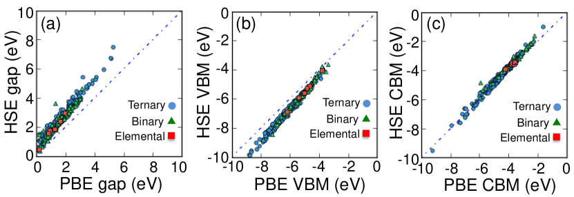
The calculated electronic properties: fundamental band gaps, VBMs, and CBMs, are shown in Fig. 2. It is known that for the semiconductor HSE band gap would scale linearly with the mixing parameter and DFT-PBE band gap value is in general the intercept. However, for materials, it is not clear how HSE band gaps are related to that predicted by DFT-PBE. Here in Fig. 2, we have illustrated that HSE band-gap values scale approximately linearly with that of DFT-PBE. The linear relation can be further improved when these isoelectronic materials are separated to different categories based on the number of constituent elements, which is reflected by color-distinguished data points in Fig. 2(a).
For absolute positions of band edges, the linear relationship between HSE and DFT-PBE is even more clear. The VBM position of a material, referenced to the vacuum level, corresponds to its electron ionization energy, which in general can be predicted by HSE to a good agreement with experiments. As shown in Fig. 2(b), HSE predicts lower VBMs than that of PBE and we also find a linear relationship between VBMs of HSE and PBE. Therefore, promisingly, PBE results may act as efficient descriptors for expensive HSE calculations, as well as experimental results, which is to be assessed in Sec. IV. Similarly, HSE CBMs also scale linearly with that obtained by PBE, illustrated in Fig. 2(c). However, for CBMs, HSE results are slightly higher than that of PBE, in sharp contrast to the case for VBMs.
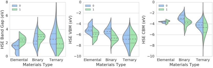
To gain deeper insights into electronic properties of this family of materials, we have shown the distribution of band gaps, VBMs, and CBMs with respect to both materials types and structural phases (Fig. 3). Clearly, for both elemental and binary materials, Phase-II structures have larger band gap values than that of Phase-I, which is closely related to the fact that VBMs of the former are in general lower than that of the later, indicated in Fig. 3(b). The similar trend for these two groups of materials can be explained by the fact that they are isoelectronic and the band-edge states are similar. On the contrary, for ternary compounds the averaged band gap value of Phase-I structures is larger than that of Phase-II structures by 1 eV; Especially, they have very similar distribution of VBMs. The different behaviors between ternary compounds from the others is due to the presence of halogen ligand that satisfied the octet rule without forming lone-pair electrons. In fact, ternary compounds are not “perfectly” isoelectronic to their parent compounds. Since the signature of long-pair electrons are still partially persevered in ternary compounds, CBMs share similar characters for all three types of materials (Fig. 3(c)). Furthermore, binary compounds are found to have larger averaged band gap than that of elemental materials, which can be attributed to the increased ionicity in the materials: a larger electronegativity difference between cation and anion usually leads to a larger band gap value Goodman (1958). The factors that affect band gaps and alignments of materials are to be discussed in Sec. IV.4.
IV Machine learning predictive models
As mentioned in Sec. II.1, computational results in present work are at two distinct levels of theory: DFT-PBE and the screened hybrid functional method (HSE). The former is computationally less demanding, but severely underestimates the fundamental band gap; HSE, on the other hand, can precisely predict band-gap values and alignments of standard semiconductors (without localized or orbitals as valence electrons), but is formidable for large-scale functional materials screening due to high computational cost. Therefore, it is desirable to build computational efficient methods that can also achieve high accuracy simultaneously. Given different predictor sets as described in Sec. II.2, we apply machine learning methods, including LR, RFR, and SVR, to predict computed electronic properties at HSE level, which can be further utilized to predict experimental observations.
IV.1 Set-I Predictors
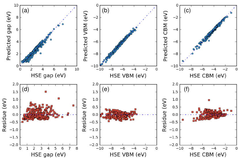
As inferred from Sec. III, HSE band gaps have approximately linear relation with that of PBE. Intuitively, PBE band gaps have been used as the only feature in Predictors Set-I. LR model is applied to model the relation between results of HSE and PBE with 10-fold cross validation, while RFR and SVR are not applicable for such simple feature space. The predicted HSE gaps of the validation sets are shown with respect to calculated values, presented in Fig. 4(a). The relation is:
| (1) |
The residues, difference between predicted and computed band-gap values, are presented in Fig. 4(d) and the majority fall into the [-0.5 eV,0.5 eV] energy range, indicating good prediction accuracy. There are only two data points where the difference is larger than 1.0 eV. Even though they might be outliers, their influence on our regression model is minimal. Furthermore, we also calculate the RMSE and MAPE to evaluate the predictive model and the small prediction error, 0.25 eV for RMSE and 10.67% for MAPE (see Table. 2), also reflects the high accuracy of the model.
Similarly, in order to predict VBMHSE positions VBMPBE values are used as the only feature in Set-I predictors space. The predicted VBMHSE positions of validation sets are presented in Fig. 4(b), showing excellent agreement with targeted values. All the residues [Fig. 4(e)] are in the [-0.5 eV,0.5 eV] energy range. The better linearity of the VBM predictive model, comparing with that of band gap, also leads to smaller prediction errors as listed in Table. 2. The predicted relationship between VBMPBE and VBMHSE is:
| (2) |
CBMHSE can also be predicted by CBMPBE with LR method and model accuracy is illustrated in Fig. 4(c) and (f). For CBM, the relation between HSE and PBE results is:
| (3) |
Since these three linear models are cross-validated by randomly selected samples from our 2D materials data set, they should be universally valid for materials that are isoelectronic to current family members.
| Regr. | Pred. | Band Gap | Band Gap | VBM | VBM | CBM | CBM |
|---|---|---|---|---|---|---|---|
| Methods | Sets | RMSE (eV) | MAPE (%) | RMSE (eV) | MAPE (%) | RMSE (eV) | MAPE (%) |
| Set-I | 0.25 | 10.67 | 0.15 | 1.85 | 0.14 | 2.53 | |
| Set-II | 0.87 | 35.07 | 0.88 | 10.30 | 0.80 | 16.03 | |
| Set-III | 0.15 | 5.55 | 0.09 | 1.04 | 0.09 | 1.56 | |
| Set-I | – | – | – | – | – | – | |
| Set-II | 0.70 | 26.37 | 0.67 | 7.23 | 0.57 | 10.22 | |
| Set-III | 0.25 | 7.44 | 0.18 | 1.75 | 0.18 | 2.64 | |
| Set-I | – | – | – | – | – | – | |
| Set-II | 0.57 | 16.80 | 0.49 | 4.83 | 0.43 | 7.07 | |
| Set-III | 0.13 | 4.93 | 0.08 | 0.96 | 0.09 | 1.65 |
IV.2 Set-II Predictors
The ideal predictive model would rather have elemental information of constituent elements as the feature space, instead of DFT results at any level of theory. This would greatly improve the model efficiency and even make real-time interactive prediction possible. We have created Predictors Set-II to fulfill such a purpose. Details about this set of predictors are discussed in Sec. II.2.
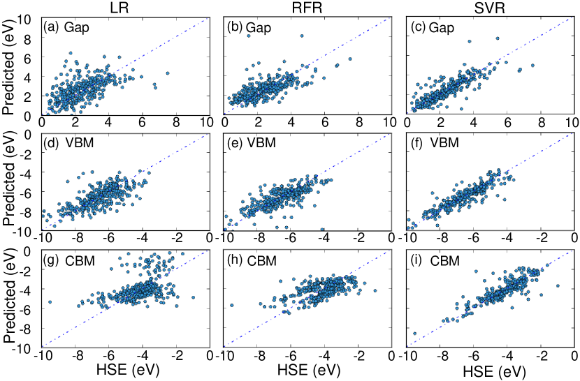
For this set of predictors, we have applied LR, RFR, and SVR to predict the targeted electronic properties. The performance of these models are shown in Fig. 5, as inferred from the relationship between predicted values and computed values.Here the LR model shows much inferior predictive ability comparing with the case when PBE results are used as predictors. This is also reflected by its high RMSE (0.87 eV) and high MAPE (35.07%) as presented in Table. 2. Comparing with band-gap prediction, the accuracy of LR model is slightly improved for VBMs and CBMs: MAPE values are 10.30% and 16.03% respectively. To avoid overfitting, we have also compared simple LR model with regularized models, such as Ridge regression and LASSO, and found no improvement in the model performance.
The undesired performance of LR model indicates that nonlinear relationship between the Set-II predictors and computed HSE results is essential. Complicated models, like RFR an SVR, are likely to capture the nonlinearity in the feature-target relation. Indeed, we find both RFR and SVR models have better performance than the former LR model. SVR is found to give the lowest RMSEs: 0.57 eV for band gaps, 0.49 eV for VBMs, and 0.43 eV for CBMs, corresponding to MAPEs of 16.80%, 4.83%, and 7.07%, which equate approximately 50% error reduction from the LR model. Even though the performance is still inferior to LR with DFT-PBE results as features, it should be noted that the SVR model we developed here is of advantage to be used for fast materials screening due to its convenient feature space with no requirements for DFT calculations.
Although RFR is not the best predictive model, it can provide precious insights on important features that determines underlying materials properties. Alongside training of a RFR model, we can also obtain the relative importance of predictors in the feature space. For band-gap prediction, the most significant feature is “Average mass”: the heavier the compounds, the smaller the band gap. It is noted that increased metallicity is inherited naturally from larger atomic mass for elements from same element group, which weakens both bonding strength and ionicity, result in the narrowing of band gap. Other important features are “Electronegativity difference between cation and anion”, “Cation electronegativity”, “Phase type”, and so on. For VBMs and CBMs, the rankings of feature importance are different: “Average mass” is not as important as for band-gap prediction. VBMs depend strongly on “Electronegativity difference between cation and anion” while “Anion electron affinity” is the most significant factor determining CBMs.
IV.3 Set-III Predictors
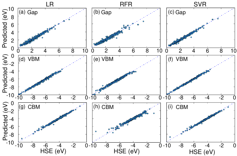
The predictive models can be further improved when predictors of Set-I and Set-II are combined as the new feature space: Set-III Predictors. As DFT-PBE can also be viewed as a good predictive model, machine learning methods based on Set-III Predictors can thus be viewed as a process of model stacking, which in general give better prediction performance. The predicted results for validation sets are compared with computed values in Fig. 6. Indeed, we find the RMSE and MAPE of all three regression models are significantly reduced with respect to the case where feature space is spanned by either Set-I or Set-II predictors. Among the machine learning models used here, SVR outperforms the other two for all three targeted materials properties, with RMSEs of 0.13 eV for band gap, 0.08 eV for VBM, and 0.09 eV for CBM. In fact, the prediction errors are within the accuracy of HSE calculations, thereby justifying the validity and accuracy of our models for properties prediction.
IV.4 Discussions
Model selection. By carefully comparing the performance of different machine learning models, we have elucidate the general principle for model selection. Both RMSE and MAPE are computed to evaluate the accuracy of LR, RFR, and SVR models. Among these three models in present study, SVR is found to have the best accuracy, when either Set-II or Set-III predictors are used as the feature space. Especially, when only elemental information is used to span the feature space, SVR show significant advantage in predicting targeted materials properties over other two methods. Therefore, SVR is suggested to use when no prior DFT-PBE results are available. On the other hand, if DFT-PBE values are available, LR is a good model to start with. In this method, the relation between HSE values and DFT-PBE features can be expressed in a simple analytical model, thus target values can be readily predicted.
Performance for different target properties. Same machine learning model is found to have different performance when target properties vary. Even though band gap is closely related to VBM and CBM, the later two targets almost always have smaller RMSE and MAPE than the former. The difference in accuracy is likely caused by the fact that for band-gap prediction a good predictor reflecting both VBM and CBM states is a requisite, which is unlikely to be included in our simple feature space. On the other hand, for VBM- or CBM-prediction the requirement is less stringent and more likely to be covered by our selection of predictors. To further improve model performance, we expect to have a more complicated feature space, including different operations between predictors in current feature space. This is beyond the scope of current study.
Applications. As mentioned in Sec. II.3, materials used in present work are just a small fraction of this large family of materials following proposed isoelectronic materials design principle. Our trained models, especially SVR with Set-II Predictors, can be applied to predict fundamental band gaps and alignments of other family members with minimal computation cost. The predicted results are informative and valuable even when the designed materials are not the most stable structural phase. It has been shown that alloying unstable materials with stable ones in the desired structural phase is likely to stabilize the former compounds. For example, CaSe can be stabilized in Phase-I when alloying with SnSe Matthews et al. (2017). The electronic properties of such alloys can also be predicted by our models where the weighted average of constituent elements are taken as predictors. Therefore, the trained machine learning models in present study provide a computational efficient method to accurately obtain band gaps and alignments of a large amount of 2D materials, which enables fast screening of 2D functional materials for electronic, optoelectronic, and photocatalysis applications.
V Conclusions
In conclusion, we have explored fundamental band gaps and alignments of a group of two-dimensional semiconductors isoelectronic to phosphorene using machine learning techniques in combination with density functional theory. This family of 2D materials shares similar crystalline structures, but possesses unprecedented rich band-gap values ranging approximately from 0 to 8 eV. Based on machine learning methods, we trained predictive models that can predict band-gap values and band-edge positions with surprisingly high accuracy. Among models discussed in present work, SVR is found to have the best performance with RMSEs less than 0.15 eV for predicted band gaps, VBMs, and CBMs when both PBE results and elemental information are used as predictors. We also demonstrate the predictive models can be utilized for electronic properties prediction for more complicated systems, like quaternary compounds and alloys, shedding light on rational materials design for (opto)electronic and photocatalysis applications.
VI Acknowledgements
This work is dedicated to Michelle Mucheng Zhu. This study was supported by the National Basic Research Program (No.2017YFA0206301) of China and the Major Program of Aerospace Advanced Manufacturing Technology Research Foundation NSFC and CASC, China (No. U1537204). Computational resources have been provided by High Performance Computing Center of the Institute of Metal Research, Chinese Academy of Sciences.
References
- Novoselov et al. (2004) K. S. Novoselov, A. K. Geim, S. V. Morozov, D. Jiang, Y. Zhang, S. V. Dubonos, I. V. Grigorieva, and A. A. Firsov, Science 306, 666 (2004).
- Zhang et al. (2005) Y. Zhang, Y.-W. Tan, H. L. Stormer, and P. Kim, Nature 438, 201 (2005).
- Mak and Shan (2016) K. F. Mak and J. Shan, Nature Photonics 10, 216 (2016).
- Fiori et al. (2014) G. Fiori, F. Bonaccorso, G. Iannaccone, T. Palacios, D. Neumaier, A. Seabaugh, S. K. Banerjee, and L. Colombo, Nature nanotechnology 9, 768 (2014).
- Radisavljevic et al. (2011) B. Radisavljevic, A. Radenovic, J. Brivio, i. V. Giacometti, and A. Kis, Nature nanotechnology 6, 147 (2011).
- Perera et al. (2013) M. M. Perera, M.-W. Lin, H.-J. Chuang, B. P. Chamlagain, C. Wang, X. Tan, M. M.-C. Cheng, D. Tománek, and Z. Zhou, ACS Nano 7, 4449 (2013), URL http://pubs.acs.org/doi/abs/10.1021/nn401053g.
- Li et al. (2014) L. Li, Y. Yu, G. J. Ye, Q. Ge, X. Ou, H. Wu, D. Feng, X. H. Chen, and Y. Zhang, Nature Nanotech. (2014).
- Liu et al. (2014) H. Liu, A. T. Neal, Z. Zhu, Z. Luo, X. Xu, D. Tomanek, and P. D. Ye, ACS Nano 8, 4033 (2014), URL http://pubs.acs.org/doi/abs/10.1021/nn501226z.
- Koenig et al. (2014) S. P. Koenig, R. A. Doganov, H. Schmidt, A. H. Castro Neto, and B. Özyilmaz, Appl. Phys. Lett. 104, 103106 (2014).
- Rodin et al. (2014) A. S. Rodin, A. Carvalho, and A. H. Castro Neto, Phys. Rev. Lett. 112, 176801 (2014), URL http://link.aps.org/doi/10.1103/PhysRevLett.112.176801.
- Ling et al. (2015) X. Ling, H. Wang, S. Huang, F. Xia, and M. S. Dresselhaus, Proceedings of the National Academy of Sciences 112, 4523 (2015).
- Liu et al. (2015) H. Liu, Y. Du, Y. Deng, and D. Y. Peide, Chemical Society Reviews 44, 2732 (2015).
- Curtarolo et al. (2013) S. Curtarolo, G. L. Hart, M. B. Nardelli, N. Mingo, S. Sanvito, and O. Levy, Nature materials 12, 191 (2013).
- De Jong et al. (2015) M. De Jong, W. Chen, T. Angsten, A. Jain, R. Notestine, A. Gamst, M. Sluiter, C. K. Ande, S. Van Der Zwaag, J. J. Plata, et al., Scientific data 2, 150009 (2015).
- Setyawan and Curtarolo (2010) W. Setyawan and S. Curtarolo, Computational Materials Science 49, 299 (2010).
- Hautier et al. (2011) G. Hautier, A. Jain, S. P. Ong, B. Kang, C. Moore, R. Doe, and G. Ceder, Chemistry of Materials 23, 3495 (2011).
- (17) https://icsd.fiz-karlsruhe.de.
- Ward and Wolverton (2017) L. Ward and C. Wolverton, Current Opinion in Solid State and Materials Science 21, 167 (2017).
- Ward et al. (2016) L. Ward, A. Agrawal, A. Choudhary, and C. Wolverton, npj Computational Materials 2, 16028 (2016).
- Deml et al. (2016) A. M. Deml, R. O’Hayre, C. Wolverton, and V. Stevanović, Physical Review B 93, 085142 (2016).
- Pilania et al. (2017) G. Pilania, J. E. Gubernatis, and T. Lookman, Computational Materials Science 129, 156 (2017).
- Lee et al. (2016) J. Lee, A. Seko, K. Shitara, K. Nakayama, and I. Tanaka, Physical Review B 93, 115104 (2016).
- Ramprasad et al. (2017) R. Ramprasad, R. Batra, G. Pilania, A. Mannodi-Kanakkithodi, and C. Kim, arXiv preprint arXiv:1707.07294 (2017).
- Balachandran et al. (2015) P. V. Balachandran, J. Theiler, J. M. Rondinelli, and T. Lookman, Scientific reports 5 (2015).
- Ji et al. (2016) J. Ji, X. Song, J. Liu, Z. Yan, C. Huo, S. Zhang, M. Su, L. Liao, W. Wang, Z. Ni, et al., Nature Communications 7, 13352 (2016).
- Zhang et al. (2016) J. L. Zhang, S. Zhao, C. Han, Z. Wang, S. Zhong, S. Sun, R. Guo, X. Zhou, C. D. Gu, K. D. Yuan, et al., Nano letters 16, 4903 (2016).
- Haleoot et al. (2017) R. Haleoot, C. Paillard, M. Mehboudi, B. Xu, L. Bellaiche, and S. Barraza-Lopez, Phys. Rev. Lett. 118, 227401 (2017).
- Fei et al. (2016) R. Fei, W. Kang, and L. Yang, Physical Review Letters 117, 097601 (2016).
- Blöchl (1994) P. Blöchl, Phys. Rev. B 50, 17953 (1994), URL http://prb.aps.org/abstract/PRB/v50/i24/p17953_1.
- Kresse and Furthmüller (1996) G. Kresse and J. Furthmüller, Phys. Rev. B 54, 11169 (1996).
- Perdew et al. (1996) J. P. Perdew, K. Burke, and M. Ernzerhof, Phys. Rev. Lett. 77, 3865 (1996), URL http://link.aps.org/doi/10.1103/PhysRevLett.77.3865.
- Hestenes and Stiefel (1952) M. R. Hestenes and E. Stiefel, J. Res. Natl. Bur. Stand. 49, 409 (1952).
- Heyd et al. (2003) J. Heyd, G. E. Scuseria, and M. Ernzerhof, J. Chem. Phys. 118, 8207 (2003), ISSN 00219606, URL http://link.aip.org/link/JCPSA6/v118/i18/p8207/s1&Agg=doi.
- Heyd et al. (2006) J. Heyd, G. E. Scuseria, and M. Ernzerhof, J. Chem. Phys. 124, 219906 (2006), ISSN 00219606, URL http://link.aip.org/link/JCPSA6/v124/i21/p219906/s1&Agg=doi.
- Monkhorst and Pack (1976) H. J. Monkhorst and J. D. Pack, Phys. Rev. B 13, 5188 (1976).
- (36) https://http://scikit-learn.org/.
- Zhu and Tománek (2014) Z. Zhu and D. Tománek, Phys. Rev. Lett. 112, 176802 (2014).
- Zhang et al. (2015) S. Zhang, Z. Yan, Y. Li, Z. Chen, and H. Zeng, Angewandte Chemie pp. 54–3112 (2015).
- Guan* et al. (2014) J. Guan*, Z. Zhu*, and D. Tománek (* equal contribution), ACS Nano 8, 12764 (2014).
- Zhu et al. (2015) Z. Zhu, J. Guan, D. Liu, and D. Tomanek, ACS Nano 9, 8284 (2015).
- Wang et al. (2017) J. Wang, B.-J. Dong, H. Guo, T. Yang, Z. Zhu, G. Hu, R. Saito, and Z.-D. Zhang, Phys. Rev. B 95, 045404 (2017).
- Goodman (1958) C. Goodman, Journal of Physics and Chemistry of Solids 6, 305 (1958).
- Matthews et al. (2017) B. E. Matthews, A. M. Holder, L. Schelhas, S. Siol, J. May, M. Forkner, D. Vigil-Fowler, M. F. Toney, J. D. Perkins, B. Gorman, et al., Journal of Materials Chemistry A (2017).