Magneto Acoustic Spin Hall Oscillators
Magneto Acoustic Spin Hall Oscillators
Abstract
This paper introduces a novel oscillator that combines the tunability of spin Hall-driven nano oscillators with the high quality factor (Q) of high overtone bulk acoustic wave resonators (HBAR), integrating both reference and tunable oscillators on the same chip with CMOS. In such magneto acoustic spin Hall (MASH) oscillators, voltage oscillations across the magnetic tunnel junction (MTJ) that arise from a spin-orbit torque (SOT) are shaped by the transmission response of the HBAR that acts as a multiple peak-bandpass filter and a delay element due to its large time constant, providing delayed feedback. The filtered voltage oscillations can be fed back to the MTJ via a) strain, b) current, or c) magnetic field. We develop a SPICE-based circuit model by combining experimentally benchmarked models including the stochastic Landau-Lifshitz-Gilbert (sLLG) equation for magnetization dynamics and the Butterworth Van Dyke (BVD) circuit for the HBAR. Using the self-consistent model, we project up to 50X enhancement in the oscillator linewidth with Q reaching up to 52825 at 3 GHz, while preserving the tunability by locking the STNO to the nearest high Q peak of the HBAR. We expect that our results will inspire MEMS-based solutions to spintronic devices by combining attractive features of both fields for a variety of applications.
Introduction
Frequency synthesizers are essential building blocks for modern communication systems such as cell phones, radio receivers, TVs, and GPS. These devices consist of a reference quartz crystal oscillator that is phase locked to a voltage controlled oscillator (VCO) through a frequency divider and are used to produce a range of stable output frequencies. However, off-chip components used to implement these devices consume large power and area. MEMS oscillators are promising candidates to replace quartz crystal oscillators in frequency synthesizers since they are CMOS-compatible, can have kHz to GHz operation, have low phase noise and excellent stability Ruby et al. (2012); Nguyen (2007); Basu and Bhattacharyya (2011); Fedder et al. (2008); Qu (2016); Li (2013); Chen et al. (2011); Fischer et al. (2016). However, they suffer from extremely limited tunability, less than 100 ppm at GHz frequencies, severely restricting their use as a single chip oscillator in the communication systems Van Beek and Puers (2011).
Recent achievements in spintronics have enabled development of nanoscale, CMOS-compatible, GHz operation, and tunable spin torque nano oscillators (STNO) Kiselev et al. (2003); Dumas et al. (2014); Chen et al. (2015, 2016); Makarov et al. (2016). These properties make STNOs promising candidates for communication applications. However, STNOs suffer from low output power and large linewidth Quinsat et al. (2010). Output power of the STNO can be improved by synchronizing a couple of STNOs or making some structural optimizations Kaka et al. (2006); Slavin and Tiberkevich (2009); Ruotolo et al. (2009); Sani et al. (2013); Locatelli et al. (2015); Lebrun et al. (2017); Banuazizi et al. (2017). Linewidth of the STNO can be reduced using various ways. Injection locking is the most well-known technique where an external signal is injected to reduce the linewidth Rippard et al. (2005); Bürgler et al. (2011); Rippard et al. (2013); Gosavi and Bhave (2015); Ganguly et al. (2016). An alternative approach is to use a self-delayed feedback in which the current of the STNO is reinjected after a certain delay, reducing the linewidth and critical current needed for oscillations Tiberkevich et al. (2014); Khalsa et al. (2015); Tsunegi et al. (2016); Dixit et al. (2012); Kumar et al. (2016); Tamaru et al. (2015); Kreissig et al. (2017); Bhuktare et al. (2017). Alternatively, a multiple peak-high Q HBAR filter is used to reduce the linewidth of the STNOs in the open loop configuration Gosavi and Bhave (2017). These methods are intended to improve the linewidth of a free running STNO. However, it is also necessary to develop a method that not only improves the linewidth but also provides the integration of the STNO and feedback components on the same chip for a single chip tunable oscillator.
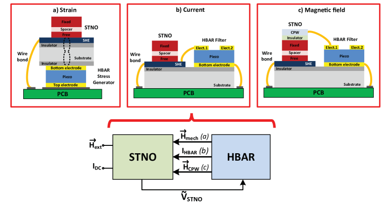
In this paper, we propose MASH oscillators that consist of a three terminal MTJ and an HBAR on the same silicon substrate with CMOS circuits, constituting a single chip oscillator. We have also shown that two-chip version of the MASH oscillators, where HBAR is implemented on a lower loss substrate, show further reduction in the linewidth at the cost of being CMOS-incompatible. Figure 1 summarizes our vision of MASH oscillators with strain, current, or magnetic field feedback. We first develop a model by solving the sLLG equation for magnetization dynamics and transport equations for spin Hall effect (SHE) and MTJ self-consistently with the BVD circuit for the HBAR in a unified SPICE based circuit platform. Each individual component of the model (sLLG, SHE, MTJ, and BVD) is experimentally benchmarked or equivalent to the-state-of the art theoretical prescription Camsari et al. (2015). Using this model, we compare the proposed MASH oscillators with a free running STNO using identical STNO and HBAR modules. MASH oscillators exhibit up to 50X enhancement in the linewidth, while maintaining the tunability by locking the STNO to the nearest high Q peak of the HBAR.
Simulation Framework
In this section, we describe our SPICE-based simulation framework consisting of sLLG and BVD modules used to implement the proposed MASH oscillator model. Identical STNO and HBAR modules are used to compare MASH oscillators with strain, current, and magnetic field feedback. Strain feedback requires an STNO and a 1-port HBAR stress generator on the opposite sides of the substrate whereas current and magnetic field feedback uses an STNO and 2-port HBAR bandpass filter on the same side.
Description of STNO and HBAR modules
STNO module.
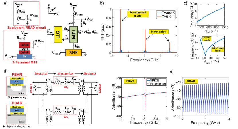
STNO consists of two ferromagnetic layers, a fixed and a free layer, separated by an insulator spacer. The free layer of the SNTO is driven into precessional dynamics by an external magnetic field and a spin polarized current that are sensed by an MTJ as voltage oscillations. We model STNOs by a standard LLG equation in the monodomain approximation using the spin-circuit framework developed in Ref. Camsari et al. (2015). The spin-circuit approach allows us to combine the SHE, MTJ, and MEMS circuits in a unified SPICE based circuit platform. Figure 2 (a) presents modular modeling of transport and magnetization dynamics for the STNOs. The time response of the magnetization along the easy axis is calculated using the sLLG equation:
| (1) |
where is the unit vector along the magnetization, is the gyromagnetic ratio, is the damping constant, is the total spin current, defined as the vectorial sum of SHE () and MTJ () components. is the total number of spins given by =V/ where is the saturation magnetization, is the volume of the free layer, is the Bohr magneton, and is the effective magnetic field including the uniaxial, shape anisotropy and magnetic thermal noise terms. The thermal noise () enters as an uncorrelated external magnetic field in three dimensions with the following mean and variance, equal in all three directions Sun et al. (2004):
| (2) |
where is the Boltzmann constant and is the temperature. In order to achieve independent control of oscillation amplitudes and frequency Liu et al. (2012), we assume that the spin current is generated by SHE where charge to spin current conversion () is expressed by Hong et al. (2016):
| (3) |
where is the spin Hall angle, and are the length and thickness, and is the spin-flip length of the SHE metal. We assume that the SHE spin-current is absorbed with 100% efficiency for simplicity and its spin polarization is along since charge flow is on and surface normal is along . Recent developments in the SHE have enabled the use of materials with large such as tungsten corresponding an efficient charge to spin current conversion Pai et al. (2012); Hao and Xiao (2015). Therefore, the conversion efficiency can exceed 1, providing an intrinsic gain. For the parameters used throughout the paper, is 2.1. We use a simple bias independent three-terminal MTJ model for CoFeB (Fixed) /MgO/CoFeB (Free)/W stack where both free and fixed CoFeB layers are magnetized in-plane in the direction, assuming a TMR of 112% with =400 and =850 . RA product of the MTJ is assumed to be 4 . Assuming an external field in the direction, the effective magnetic field becomes =(+ ) +. We have also assumed that the stray field due to the fixed layer is subsumed into the externally applied field, since these are along the same direction. Voltage oscillations across the MTJ can be expressed as:
| (4) |
where Camsari et al. (2014), is average MTJ conductance ([+]/2), is polarization, , and the read voltage and resistance. The fixed layer contribution to the spin-current is: . The resistance contribution of the SHE is neglected in the equivalent read circuit since the MTJ resistance is the dominant resistance in this path. Figure 2 (b) shows simulated FFT (Fast Fourier Transform) spectrums of a free running STNO at T=300 K and T=0 K (noiseless) for =23 mV, showing the fundamental mode and harmonics. Figure 2 (c) shows the tunability of the STNO that can be independently controlled by and . The oscillation frequency increases with the square root of the external magnetic field at low fields and linearly at high fields as predicted by the Kittel equation . Alternatively, the oscillation frequency can be tuned by a charge current passing through SHE metal generating a spin current on the free layer. There are two main modes of vibration for the STNOs: in-plane and out-of plane modes. In the in-plane mode, frequency decreases as increases whereas the opposite is valid for the out-of-plane mode Kiselev et al. (2003). In order to sustain periodic oscillations, the spin-torque needs to exceed a critical value to overcome the damping terms, which in this work corresponds to a of 15 mV. There are no oscillations below this value. STNO operation requires the spin-torque current and external field to be in anti-parallel directions to sustain continuous oscillations. Therefore simply changing the polarity of the tuning voltage to negative values do not result in oscillations (and hence not shown), unless the magnetic field direction is also reversed.
HBAR module.
HBAR is a key element in MASH oscillators since it provides high Q resonance peaks, enabling high Q filtering with an effective delay and maintaining tunability of the STNO. The HBAR consists of a piezoelectric layer sandwiched between two electrodes on an acoustic substrate. The piezoelectric film acts as a transducer to generate standing waves at several wavelengths through the acoustic substrate. The acoustic substrate acts as a resonant cavity so that several resonance peaks occur that are separated from each other by a known frequency spacing, . We use different HBAR designs with a 1 m AlN layer on top of a 100 m and 200 m thick silicon substrates: a) 1-port HBAR stress generator for the strain feedback and b) 2-port HBAR filter to implement the current and magnetic feedback. The frequency of the HBAR is where n is number of the acoustic modes, is silicon thickness, and are the Young’s modulus and density of the silicon. We neglect the contribution of AlN layer on the equivalent mass and spring constant in the model since HBAR is mostly formed by the silicon substrate. This assumption is valid as long as the thicknesses of the piezoelectric film is much smaller than the thickness of the substrate. The fundamental mode of the HBAR is when a full wavelength fits to the AlN layer, . Total number of the modes can be found by where , which is equal to 101 modes that are separated by ==43 MHz for a 100 m thick HBAR design. Figure 2 (d) presents the BVD circuit model of the HBAR where each acoustic mode is defined as a separate RLC circuit Tilmans (1996). The mechanical equivalent of , , and is the damping constant (), equivalent mass (), and inverse of equivalent spring constant (1/), respectively. The is also equal to where is the mechanical quality factor of a defined mode. We have experimentally shown that the product of a silicon HBAR is approximately in Gosavi et al. (2015) which provides Q of 2500-5000 within the frequency range of 2-4 GHz for the model. The and can be calculated by:
| (5) |
The electrical to mechanical conversion in the BVD circuit is expressed by two transformers where and are the transduction factors, which are typically equal to each other (==) for symmetric structures where where is the out-of plane piezoelectric coefficient of AlN, is the area of the HBAR, is the thickness of the AlN film Tilmans (1996). The capacitance between the top and bottom electrodes of the HBAR is equal to where and are the dielectric constant of the free space and AlN layer.
The BVD circuit can be used to model 1-port stress HBAR generator by removing the transformer at the output. Therefore, the output current of the HBAR becomes equal to the mechanical velocity and can be converted to the mechanical displacement () with an integrator. Assuming the stress is uniform through the substrate, strain is approximately equal to =. The 2-port HBAR is modeled using the BVD circuit with two output electrodes. The 2-port configuration can be explained by two coupled HBAR devices where transmission loss is determined by the gap between the electrodes. We use identical parameters for both 1-port and 2-port HBAR designs in order to make an accurate comparison between different feedback methods. Figure 2 (e) compares admittance plots of a film bulk acoustic wave resonator (FBAR) and a 2-port HBAR, consistent with the Equation (8) and our experimental results in Gosavi et al. (2015); Gosavi and Bhave (2017). Unlike an FBAR, HBAR has multiple high Q resonance peaks that are spaced by =43 MHz for a 100 m thick silicon substrate. The HBAR has a large time constant and acts as a delay element where the effective delay can be calculated as , which is 330 ns at 3 GHz with a Q of 3000.
Results
MASH oscillator with strain feedback
Figure 3 (a-b) shows the block diagram and modular modeling of MASH oscillator implemented with an STNO and a 1-port HBAR stress generator on the opposite sides of the silicon substrate with strain feedback. Magnetization of the free layer is controlled using an AC stress generated by the HBAR with magnetostriction effect Gowtham et al. (2016, 2015); Khan et al. (2014); Roy et al. (2012). In the presence of a uniaxial mechanical stress and external magnetic field in the and directions, effective magnetic field becomes =( + ) +. The periodic oscillations on the free layer is sensed by the MTJ as an oscillation voltage. This voltage is amplified by a gain stage to bias the HBAR in order to generate sufficient amount of stress in the direction. Output current of the HBAR driven by the STNO can be written as:
| (6) |
When driven at resonance (==1/), HBAR becomes a low impedance path with ()=/. Therefore, the output current becomes =()/ and equal to the mechanical velocity (=). The mechanical velocity can be converted to the mechanical displacement () with a simple integration. Assuming that the stress is uniform through the substrate, the strain () approximately is equal to =. The strain injects an AC magnetic field on the free layer via Gowtham et al. (2015): where is the magnetoelastic coupling coefficient. The magnetoelastic coupling coefficient for 2 nm CoFeB is measured to be erg/ in Gowtham et al. (2016), and the HBAR can generate AC strain in the range of 20-200 ppm depending on the output voltage of the SNTO and amplifier gain. This amount of strain injects an AC magnetic field of 4.5-45 on the free layer.
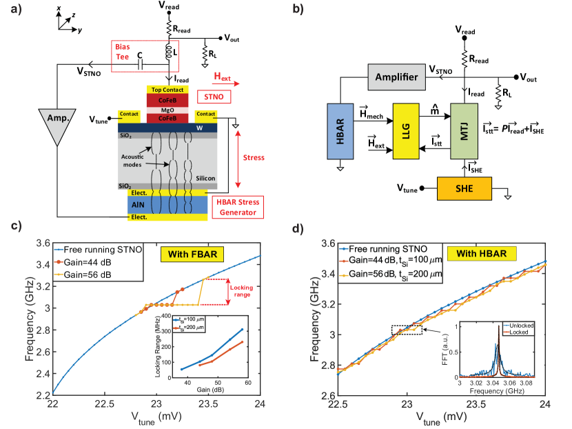
The injected magnetic field causes a phase shift in the STNO and the oscillation frequency changes to compensate the phase shift, causing the locking. When locked, the phase of the STNO follows the phase of the injection signal Adler (1946); Razavi (2004). Since the HBAR continuously cleans the STNO signal and generates a high Q injection signal in the loop, the linewidth of the STNO improves with the simultaneous effect of high Q filtering and delayed feedback by the HBAR. Figure 3(c) presents the locking range of the STNO for different amplifier gains and substrate thicknesses (100 m and 200 m) simulated with an FBAR. The locking range can be calculated by using Adler’s equation:
| (7) |
where is the maximum locking range, is oscillation frequency, is quality factor, is oscillation current, and is injected signal for the locking. Equation (7) can be simplified to =(/2)(/) if , predicting a linear locking range with increased . However, MASH oscillator produces its own by driving the HBAR at or near resonance. Therefore, does not linearly increase with increased amplifier gain, showing a non-linear locking range. Amplifier gain can be reduced by increasing the output voltage of the STNO or using a material stack with higher magnetostrictive and piezoelectric coefficients. The substrate thickness () also affects the gain needed for locking since the thicker substrate (=200 m) can generate lower strain.
Figure 3 (d) presents tunability of MASH oscillator with the strain feedback where the STNO is locked to the nearest peak of the HBAR that are separated by 43 MHz for a 100 m thick HBAR. Therefore, MASH oscillator can be tuned with 43 MHz steps by changing . When locked, MASH oscillator demonstrates a significant enhancement in the linewidth with the combination of high Q filtering and delayed feedback. The tuning step can be decreased if the spacing between the HBAR modes are reduced. For instance, separation between the modes becomes 22 MHz when is 200 m, showing a step tunability of 22 MHz. However, this also decreases the amount of stress generated by the HBAR, requiring higher amplifier gain for the feedback as shown in the Figure 3 (d).
MASH oscillator with current feedback
Figure 4 (a-b) presents the implementation of MASH oscillator with a three-terminal MTJ and a 2-port HBAR using the current feedback. Voltage across the MTJ is amplified by a gain stage and filtered by a 2-port HBAR filter, allowing the signal transmission only at its sharp resonance peaks. The filtered current output of the HBAR can be expressed as:
| (8) |
where is amplifier gain, is the frequency of the HBAR, and is the output voltage of the STNO. When driven at resonance (==), HBAR becomes a low impedance path with ()=/. Therefore, the injected AC current is =( )/(+) that is used to generate an AC spin current through the SHE metal (=), causing an injection locking. Even though the geometric factor (/) in Equation (3) can be used to provide an intrinsic gain in the loop, this gain is not sufficient. Therefore, an additional amplifier is used to compensate the transmission losses and provide the gain necessary for the feedback.
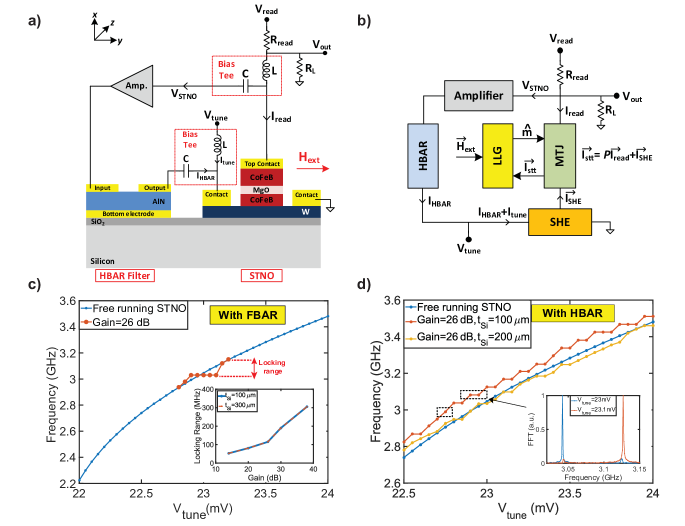
Figure 4 (c) presents the locking range of the STNO for different amplifier gains and substrate thicknesses (100 m and 200 m) simulated with an FBAR. Similar to strain feedback, we do not have a linear locking range since shows non-linear characteristics by driving the HBAR at or near resonance. Nevertheless, the simulation results seem consistent with Equation (7) and experimental results where injection locking is achieved by an external current source Rippard et al. (2005, 2013). Compared to the strain feedback, a lower amplifier gain is sufficient to reach a similar locking range and it does not depend on the substrate thickness (), proving that the current feedback is more efficient. Amplifier gain can further be decreased by reducing the transmission loss that depends on the lateral spacing between the input and output electrodes of the HBAR. Figure 4 (d) shows the tunability of MASH oscillator where the output frequency can be tuned with 43 MHz steps by changing for a 100 m thick HBAR similar to the strain feedback. Using a thicker substrate (=200 m) reduces the separation (=22 MHz) between the HBAR modes, and this enables a tunability with 22 MHz steps without increasing the amplifier gain.
MASH oscillator with magnetic field feedback
Figure 5 (a-b) shows the implementation and circuit model of MASH oscillator with an STNO including a CPW and a 2-port HBAR filter using the magnetic field feedback. Voltage oscillations across the MTJ is shaped by the HBAR. Output current of the HBAR is passed through the CPW after a certain delay to injects an AC magnetic field on the free layer, providing the magnetic field feedback. In the presence of the magnetic feedback, effective field becomes =( + ) +. Neglecting the effect of layers between the CPW and free layer, can be approximately expressed as inDixit et al. (2012); Kumar et al. (2016): where is the AC current passed through the CPW. When driven at resonance (==), HBAR becomes a low impedance path with ()=/. Therefore, the AC current becomes =( )/(+) that is used to generate an AC magnetic field through the CPW where is assumed to be 1k. Similarly, the generated magnetic field causes a phase shift and oscillation frequency changes to compensate the phase shift. Therefore, the combination of high Q filtering and delayed feedback improves the linewidth significantly. Moreover, this approach provides the most efficient feedback approach even though it requires additional process steps to fabricate the CPW on top of the MTJ. It also provides an electrical isolation between the MTJ and HBAR while achieving the feedback.
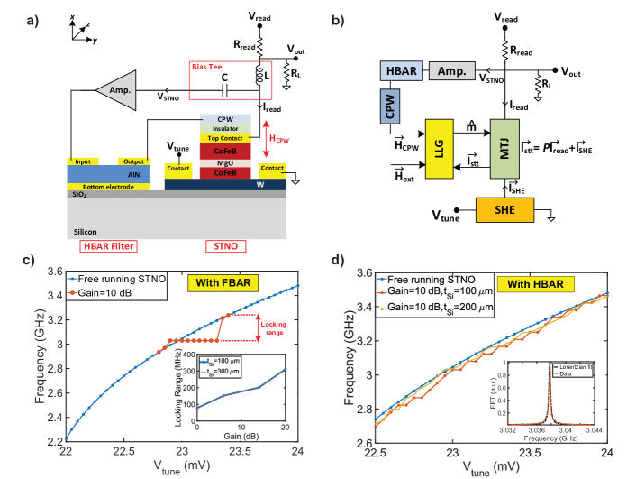
Figure 5 (c) presents the locking range for different amplifier gains and substrate thicknesses (100 m and 200 m) simulated with an FBAR using the magnetic field feedback. Gain stage is only used to compensate the transmission losses of the HBAR and even a gain of 10 dB is sufficient for the feedback, much lower compared to other feedback methods. The locking range is independent of the substrate thickness and it is not necessary to increase the amplifier gain for thicker substrates (=200 m) unlike the strain feedback. Figure 5 (d) shows the tunability of MASH oscillator with magnetic feedback where the tunability is provided with 22 MHz or 43 MHz steps depending on the substrate thickness (=100 m or 200 m) by locking the STNO to the nearest resonance peak of the HBAR.
Discussion
| Feedback | Implementation | Gain | Linewidth | Osc. | CMOS Compatible |
| Free running | 3-T MTJ | N/A | 2.7 MHz | 1147 | Yes, single chip |
| Strain | 3-T MTJ-1 port HBAR | 44 dB | 191 kHz | 15834 | Yes, single chip |
| Current | 3-T MTJ-2 port HBAR | 26 dB | 293 kHz | 10376 | Yes, single chip |
| Current | 3-T MTJ-2 port Sapphire HBAR | 26 dB | 55 kHz | 52825 | No, two chips |
| Magnetic | 3-T MTJ-2 port HBAR- CPW | 10 dB | 186 kHz | 12274 | Yes, single chip |
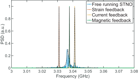
In this paper, we proposed a new class of microwave oscillators combining the tunability of a free running STNO with high Q of HBAR, integrating both reference and tunable oscillators on the same chip with CMOS circuits. Proposed MASH oscillators are composed of a high Q HBAR reference oscillator that is locked to a three-terminal MTJ through strain, current, or magnetic field feedback. HBAR filters voltage oscillations across the MTJ and reinjects the cleaned signal after a certain delay, causing a delayed feedback without requiring an additional source or an external delay element. Figure 6 compares simulated FFT spectrums of a free running STNO with MASH oscillators using different feedback methods. The combination of high Q filtering and delayed feedback exhibits a 15X enhancement in the linewidth as a single chip oscillator, reaching a Q up to 15834 at 3 GHz whereas the free running STNO has a Q of 1147.
Table 1 summarizes the results with a free running STNO and MASH oscillators, considering the different feedback methods, amplifier gain, oscillator linewidth and oscillator Q. Strain feedback provides a solution where single or multiple STNOs can be controlled with a single HBAR at the cost of larger amplifier gain whereas current and magnetic field feedback are more energy efficient and do not require any magnetostrictive materials. The CoFeB and AlN stacks used in this work do not have high magnetostriction and piezoelectric coefficients to generate a sufficient amount of magnetic field without an amplifier. Selection of materials with higher magnetostrictive and piezoelectric coefficients such as Terfenol and PZT may generate higher magnetic field Roy et al. (2012); Khan et al. (2014); Gowtham et al. (2015), reducing the amplifier gain necessary for the feedback. However, the use of CoFeB and AlN layers is still a good choice since they are well optimized and CMOS compatible.
Proper choice of the acoustic substrate is essential in order to implement a high Q HBAR since Q of the HBAR depends on the acoustic losses in the piezoelectric film and substrate. Use of a lower loss substrate such as sapphire significantly increases the Q of the HBAR up to 22,000 as experimentally observed in one of our earlier worksGosavi and Bhave (2017), also increasing the Q of the MASH oscillator. We have shown a 50X enhancement in the linewidth with two-chip version of the MASH oscillators using the sapphire HBAR in Gosavi et al. (2015) at the cost of being CMOS-incompatible.
It is also crucial to maintain the tunability of the standard STNO while improving the linewidth. The tunability has been preserved by locking the STNO to the nearest peak of the HBAR where the substrate thickness determines the tuning-steps by defining the spacing between the HBAR modes.
| Parameters | Value |
|---|---|
| 100 nm 60 nm 2 nm | |
| , | 800 emu/, 0.01 |
| , | 200 Oe, 10000 Oe |
| , | 400 , 0.6 |
| , | 400 , 50 |
| , , Hao and Xiao (2015) | 0.4, 3.5 nm, 210 |
| , , Hao and Xiao (2015) | 60 nm, 100 nm, 9 nm |
| Gowtham et al. (2016) | erg/ |
| , , | 300 Oe, 10 mV, 15-50 mV |
| , , , | 170 GPa, 2330 g/, 9, 1.55 C/ |
| , | 75 m, 1 m |
| , | 100 nm, 1 k |
| , (SPICE) | 10 s, 0.1 ps |
| , , (FFT) | 0.1 MHz, 13.1 GHz, 262144 |
Methods
MASH oscillators are implemented by combining the sLLG equation for magnetization dynamics and transport equations for SHE and MTJ self-consistently with the BVD circuit for the HBAR using the modular approach framework Camsari et al. (2015). HSPICE is used to solve the coupled differential equations of the oscillator network simultaneously. All simulations are done using the transient noise analysis in HSPICE with a simulation time of = 10 s and a step time of =0.1 ps. is selected as small as possible to completely eliminate numerical noise in the simulations. Frequency spectrum is obtained by taking the FFT of the time domain signal. Initial 0.1 s of the data is excluded while converting the time domain signal to the FFT. The minimum and maximum frequency of FFT are calculated by and where is number of points. In our simulations, we used =0.1 MHz and =13.1 GHz for N=262144. PSD is plotted by having the square of absolute of FFT. Linewidth (f) of the oscillators is extracted by fitting a Lorentzian function to the PSD data, and Q is calculated using /f. Table 2 presents device and material parameters used in all simulations.
References
- Ruby et al. (2012) Ruby, R.; Small, M.; Bi, F.; Lee, D.; Callaghan, L.; Parker, R.; Ortiz, S. IEEE transactions on ultrasonics, ferroelectrics, and frequency control 2012, 59, 334–345.
- Nguyen (2007) Nguyen, C. T.-C. IEEE transactions on ultrasonics, ferroelectrics, and frequency control 2007, 54.
- Basu and Bhattacharyya (2011) Basu, J.; Bhattacharyya, T. K. Microsystem Technologies 2011, 17, 1557.
- Fedder et al. (2008) Fedder, G. K.; Howe, R. T.; Liu, T.-J. K.; Quevy, E. P. Proceedings of the IEEE 2008, 96, 306–322.
- Qu (2016) Qu, H. Micromachines 2016, 7, 14.
- Li (2013) Li, S.-S. CMOS-MEMS resonators and their applications. European Frequency and Time Forum & International Frequency Control Symposium (EFTF/IFC), 2013 Joint. 2013; pp 915–921.
- Chen et al. (2011) Chen, W.-C.; Fang, W.; Li, S.-S. Journal of Micromechanics and Microengineering 2011, 21, 065012.
- Fischer et al. (2016) Fischer, A. C.; Forsberg, F.; Lapisa, M.; Bleiker, S. J.; Stemme, G.; Roxhed, N.; Niklaus, F. arXiv preprint arXiv:1604.04843 2016,
- Van Beek and Puers (2011) Van Beek, J.; Puers, R. Journal of Micromechanics and Microengineering 2011, 22, 013001.
- Kiselev et al. (2003) Kiselev, S. I.; Sankey, J.; Krivorotov, I.; Emley, N.; Schoelkopf, R.; Buhrman, R.; Ralph, D. Nature 2003, 425, 380–383.
- Dumas et al. (2014) Dumas, R. K.; Sani, S. R.; Mohseni, S. M.; Iacocca, E.; Pogoryelov, Y.; Muduli, P. K.; Chung, S.; Durrenfeld, P.; Akerman, J. IEEE transactions on magnetics 2014, 50, 1–7.
- Chen et al. (2015) Chen, T.; Eklund, A.; Sani, S.; Rodriguez, S.; Malm, B. G.; Åkerman, J.; Rusu, A. Solid-State Electronics 2015, 111, 91–99.
- Chen et al. (2016) Chen, T.; Dumas, R. K.; Eklund, A.; Muduli, P. K.; Houshang, A.; Awad, A. A.; Dürrenfeld, P.; Malm, B. G.; Rusu, A.; Åkerman, J. Proceedings of the IEEE 2016, 104, 1919–1945.
- Makarov et al. (2016) Makarov, A.; Windbacher, T.; Sverdlov, V.; Selberherr, S. Semiconductor Science and Technology 2016, 31, 113006.
- Quinsat et al. (2010) Quinsat, M.; Gusakova, D.; Sierra, J.; Michel, J.; Houssameddine, D.; Delaet, B.; Cyrille, M.-C.; Ebels, U.; Dieny, B.; Buda-Prejbeanu, L.; Katine, J.; Zeltser, A.; Prigent, M.; Nallatamby, J.; Sommet, R. Applied Physics Letters 2010, 97, 182507.
- Kaka et al. (2006) Kaka, S.; Pufall, M. R.; Rippard, W. H.; Silva, T. J.; Russek, S. E.; Katine, J. A. Mutual phase-locking of microwave spin torque nano-oscillators. Magnetics Conference, 2006. INTERMAG 2006. IEEE International. 2006; pp 2–2.
- Slavin and Tiberkevich (2009) Slavin, A.; Tiberkevich, V. IEEE Transactions on Magnetics 2009, 45, 1875–1918.
- Ruotolo et al. (2009) Ruotolo, A.; Cros, V.; Georges, B.; Dussaux, A.; Grollier, J.; Deranlot, C.; Guillemet, R.; Bouzehouane, K.; Fusil, S.; Fert, A. Nature nanotechnology 2009, 4, 528–532.
- Sani et al. (2013) Sani, S.; Persson, J.; Mohseni, S. M.; Pogoryelov, Y.; Muduli, P.; Eklund, A.; Malm, G.; Käll, M.; Dmitriev, A.; Åkerman, J. Nature communications 2013, 4.
- Locatelli et al. (2015) Locatelli, N.; Hamadeh, A.; Araujo, F. A.; Belanovsky, A. D.; Skirdkov, P. N.; Lebrun, R.; Naletov, V. V.; Zvezdin, K. A.; Muñoz, M.; Grollier, J.; Klein, O.; Cros, V.; Loubens, G. Scientific reports 2015, 5.
- Lebrun et al. (2017) Lebrun, R.; Tsunegi, S.; Bortolotti, P.; Kubota, H.; Jenkins, A.; Romera, M.; Yakushiji, K.; Fukushima, A.; Grollier, J.; Yuasa, S.; Cros, V. Nature Communications 2017, 8.
- Banuazizi et al. (2017) Banuazizi, S. A. H.; Sani, S. R.; Eklund, A.; Naiini, M. M.; Mohseni, S. M.; Chung, S.; Dürrenfeld, P.; Malm, B. G.; Åkerman, J. Nanoscale 2017, 9, 1896–1900.
- Rippard et al. (2005) Rippard, W. H.; Pufall, M. R.; Kaka, S.; Silva, T. J.; Russek, S. E.; Katine, J. A. Physical review letters 2005, 95, 067203.
- Bürgler et al. (2011) Bürgler, D. E.; Sluka, V.; Lehndorff, R.; Deac, A. M.; Kákay, A.; Hertel, R.; Schneider, C. M. Injection locking of single-vortex and double-vortex spin-torque oscillators. SPIE NanoScience+ Engineering. 2011; pp 810018–810018.
- Rippard et al. (2013) Rippard, W.; Pufall, M.; Kos, A. Applied Physics Letters 2013, 103, 182403.
- Gosavi and Bhave (2015) Gosavi, T. A.; Bhave, S. A. Model for acoustic locking of Spin Torque Oscillator. Frequency Control Symposium the European Frequency and Time Forum (FCS), 2015 Joint Conference of the IEEE International. 2015; pp 68–71.
- Ganguly et al. (2016) Ganguly, S.; Torunbalci, M. M.; Bhave, S. A.; Camsari, K. Y. MESH Nano-Oscillator: All electrical doubly tunable spintronic oscillator. Device Research Conference (DRC), 2016 74th Annual. 2016; pp 1–2.
- Tiberkevich et al. (2014) Tiberkevich, V. S.; Khymyn, R. S.; Tang, H. X.; Slavin, A. N. Scientific reports 2014, 4.
- Khalsa et al. (2015) Khalsa, G.; Stiles, M.; Grollier, J. Applied Physics Letters 2015, 106, 242402.
- Tsunegi et al. (2016) Tsunegi, S.; Grimaldi, E.; Lebrun, R.; Kubota, H.; Jenkins, A. S.; Yakushiji, K.; Fukushima, A.; Bortolotti, P.; Grollier, J.; Yuasa, S.; Cros, V. Scientific reports 2016, 6.
- Dixit et al. (2012) Dixit, D.; Konishi, K.; Tomy, C.; Suzuki, Y.; Tulapurkar, A. Applied Physics Letters 2012, 101, 122410.
- Kumar et al. (2016) Kumar, D.; Konishi, K.; Kumar, N.; Miwa, S.; Fukushima, A.; Yakushiji, K.; Yuasa, S.; Kubota, H.; Tomy, C.; Prabhakar, A.; Suzuki, Y.; A, T. Scientific reports 2016, 6, 30747.
- Tamaru et al. (2015) Tamaru, S.; Kubota, H.; Yakushiji, K.; Yuasa, S.; Fukushima, A. Scientific reports 2015, 5.
- Kreissig et al. (2017) Kreissig, M.; Lebrun, R.; Protze, F.; Merazzo, K.; Hem, J.; Vila, L.; Ferreira, R.; Cyrille, M.; Ellinger, F.; Cros, V.; U, E.; P, B. AIP Advances 2017, 7, 056653.
- Bhuktare et al. (2017) Bhuktare, S.; Singh, H.; Bose, A.; Tulapurkar, A. A. Physical Review Applied 2017, 7, 014022.
- Gosavi and Bhave (2017) Gosavi, T. A.; Bhave, S. A. Magneto-acoustic oscillator. Solid-State Sensors, Actuators and Microsystems (TRANSDUCERS), 2017 19th International Conference on. 2017; pp 448–451.
- Camsari et al. (2015) Camsari, K. Y.; Ganguly, S.; Datta, S. Scientific reports 2015, 5, 10571.
- Sun et al. (2004) Sun, J. Z.; Kuan, T.; Katine, J.; Koch, R. H. Spin angular momentum transfer in a current-perpendicular spin-valve nanomagnet. Integrated Optoelectronic Devices 2004. 2004; pp 445–455.
- Liu et al. (2012) Liu, L.; Pai, C.-F.; Ralph, D.; Buhrman, R. Physical review letters 2012, 109, 186602.
- Hong et al. (2016) Hong, S.; Sayed, S.; Datta, S. IEEE Transactions on Nanotechnology 2016, 15, 225–236.
- Pai et al. (2012) Pai, C.-F.; Liu, L.; Li, Y.; Tseng, H.; Ralph, D.; Buhrman, R. Applied Physics Letters 2012, 101, 122404.
- Hao and Xiao (2015) Hao, Q.; Xiao, G. Physical Review Applied 2015, 3, 034009.
- Camsari et al. (2014) Camsari, K. Y.; Ganguly, S.; Datta, D.; Datta, S. Physics-based factorization of magnetic tunnel junctions for modeling and circuit simulation. Electron Devices Meeting (IEDM), 2014 IEEE International. 2014; pp 35–6.
- Tilmans (1996) Tilmans, H. A. Journal of Micromechanics and Microengineering 1996, 6, 157.
- Gosavi et al. (2015) Gosavi, T. A.; MacQuarrie, E. R.; Fuchs, G. D.; Bhave, S. A. HBAR as a high frequency high stress generator. Ultrasonics Symposium (IUS), 2015 IEEE International. 2015; pp 1–4.
- Gowtham et al. (2016) Gowtham, P. G.; Stiehl, G. M.; Ralph, D. C.; Buhrman, R. A. Physical Review B 2016, 93, 024404.
- Gowtham et al. (2015) Gowtham, P. G.; Rowlands, G. E.; Buhrman, R. A. Journal of Applied Physics 2015, 118, 183903.
- Khan et al. (2014) Khan, A.; Nikonov, D. E.; Manipatruni, S.; Ghani, T.; Young, I. A. Applied Physics Letters 2014, 104, 262407.
- Roy et al. (2012) Roy, K.; Bandyopadhyay, S.; Atulasimha, J. Journal of Applied Physics 2012, 112, 023914.
- Gowtham et al. (2015) Gowtham, P. G.; Moriyama, T.; Ralph, D. C.; Buhrman, R. A. Journal of Applied Physics 2015, 118, 233910.
- Adler (1946) Adler, R. Proceedings of the IRE 1946, 34, 351–357.
- Razavi (2004) Razavi, B. IEEE Journal of Solid-State Circuits 2004, 39, 1415–1424.