Structure of Native Two-dimensional Oxides on III–Nitride Surfaces
When pristine material surfaces are exposed to air, highly reactive broken bonds can promote the formation of surface oxides with structures and properties differing greatly from bulk. Determination of the oxide structure, however, is often elusive through the use of indirect diffraction methods or techniques that probe only the outer most layer. As a result, surface oxides forming on widely used materials, such as group III-nitrides, have not been unambiguously resolved, even though critical properties can depend sensitively on their presence. In this work, aberration corrected scanning transmission electron microscopy reveals directly, and with depth dependence, the structure of native two–dimensional oxides that form on AlN and GaN surfaces. Through atomic resolution imaging and spectroscopy, we show that the oxide layers are comprised of tetrahedra–octahedra cation–oxygen units, similar to bulk –Al2O3 and –Ga2O3. By applying density functional theory, we show that the observed structures are more stable than previously proposed surface oxide models. We place the impact of these observations in the context of key III-nitride growth, device issues, and the recent discovery of two-dimnesional nitrides.
Group III–nitrides, such as GaN and AlN, are the bedrock of modern solid–state lighting. Further, they are of particular interest for high power devices because of their strong polarization fields that can confine carriers to heterointerfaces supplied via extrinsic doping or surface states (?). At the surface of the III-nitrides, however, dangling bonds are reactive to their environment (?, ?, ?), and lead to the formation of surface oxides. Importantly, the surface structure has been proposed to play an important role in controlling the electronic properties of buried device structures. For example, in power electronic devices, surface compensation can have a dramatic influence on the mobility of the two-dimensional electron gas (2DEG) that forms at AlGaN/GaN heterointerfaces (?, ?, ?, ?).
While further advancements require complete understanding of the native surface oxides, much remains unknown about their structure (?, ?, ?, ?, ?). Methods such as X-ray photoelectron or Auger electron spectroscopies and electron diffraction (?) provide key insights, but are an indirect probe. While scanning tunneling microscopy can probe the surface atomic and electronic structure, the outer most valence electrons are primarily probed. As a result, surface oxide structural models have thus largely relied on presumed atomic configurations paired with first principles density functional theory (DFT) calculations to estimate relative stability of each model (?, ?). As a result, there are a number of competing surface oxide models that can be difficult or impossible to determine without direct surface and sub-surface information from experiment.
Here, we report the direct observation of native two–dimensional oxides that form on III–nitride surfaces. Using aberration corrected scanning transmission electron microscopy (STEM) imaging and spectroscopy, the structure of these two-dimensional oxides is directly determined for c–plane AlN and GaN surfaces. The observed oxides differ considerably from bulk structures, but with bonding configurations consistent with the corresponding group III oxide. Furthermore, these oxides are found to be more energetically stable than previous surface oxide models over a wide range of chemical environments. Finally, the structures are discussed in the context of material growth and properties.

Direct, atomic resolution annular dark-field (ADF) STEM reveals the formation of a surface layer on c–plane AlN and GaN as shown in Figure 1. For both materials, the surface is comprised of a two–dimensional layer that forms across the c-plane sample surface. The layer is distinguished by a trilayer (dashed boxed regions) and an inverted bilayer (solid boxes) in Figures 1A and B. The outer surface is consistent with prior oxide formation studies using indirect methods and STM, but those methods could not resolve the sub-surface information (?). Furthermore, the layered structure appears passivated as further growth of the oxide does not occur over time. Also, as discussed in the Supplementary Information, various approaches to the TEM sample preparation were attempted to rule out unintentional modification of the surface. Regardless of the preparation approach, the observed surface structure remained the same.
While atom column positions can be directly determined from the ADF STEM images, the atomic species can be difficult or impossible to identify without additional information (?). For unambiguous elemental analysis, we turn to electron energy loss spectroscopy (EELS), where an abrupt transition from the nitride to a two-dimensional oxide layer is seen in Figure 2. Furthermore, the oxygen signal extends into the nitride beyond the surface oxide, which may indicate oxygen–nitrogen intermixing, delocalization of the electron probe, and/or oxide formation on the top/bottom of the TEM sample. Note that EELS of the GaN surface exhibits the same distribution of anions, as shown in Figure S1.

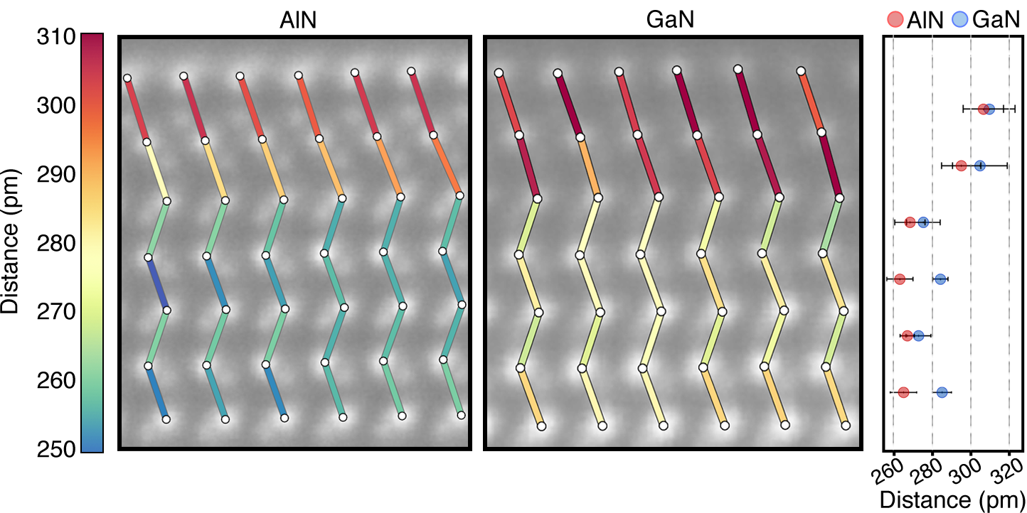
Distance measurements from the perpendicular view directions in Figure 1 are used to construct a three dimensional model of the oxides. Through use of revolving STEM (?), accurate and precise (?) atom column distance measurements for AlN are included in Figure 3. The projected Al–N distances measured in the AlN substrate agree with those (expected) from bulk: 109 pm (107 pm) and 191 pm (192 pm). At the nitride/oxide interface, the first Al–O bond length is 176 pm. This length is consistent with the shorter bonds in bulk Al oxide, Al–O 175 pm (?), than the nitrides. In the middle of the trilayer, the projected Al–O distance is 138 pm (Figure 3A,B). A comparison to GaN distance measurements is provided in Figure S3. In addition, in–plane distances between adjacent Al/Ga and N/O columns gradually decreases, as shown in Figure S2.
To probe bond angles, the angle between neighboring anions on (0001) planes and the nearest group III atom column are measured, as shown for AlN in Figure 3 (C,D). The average angles are 34∘ and 48∘ for the AlN bulk and oxide, respectively. These are consistent the projected angles from wurtzite and Al2O3, which are 35∘ and 52∘, respectively.
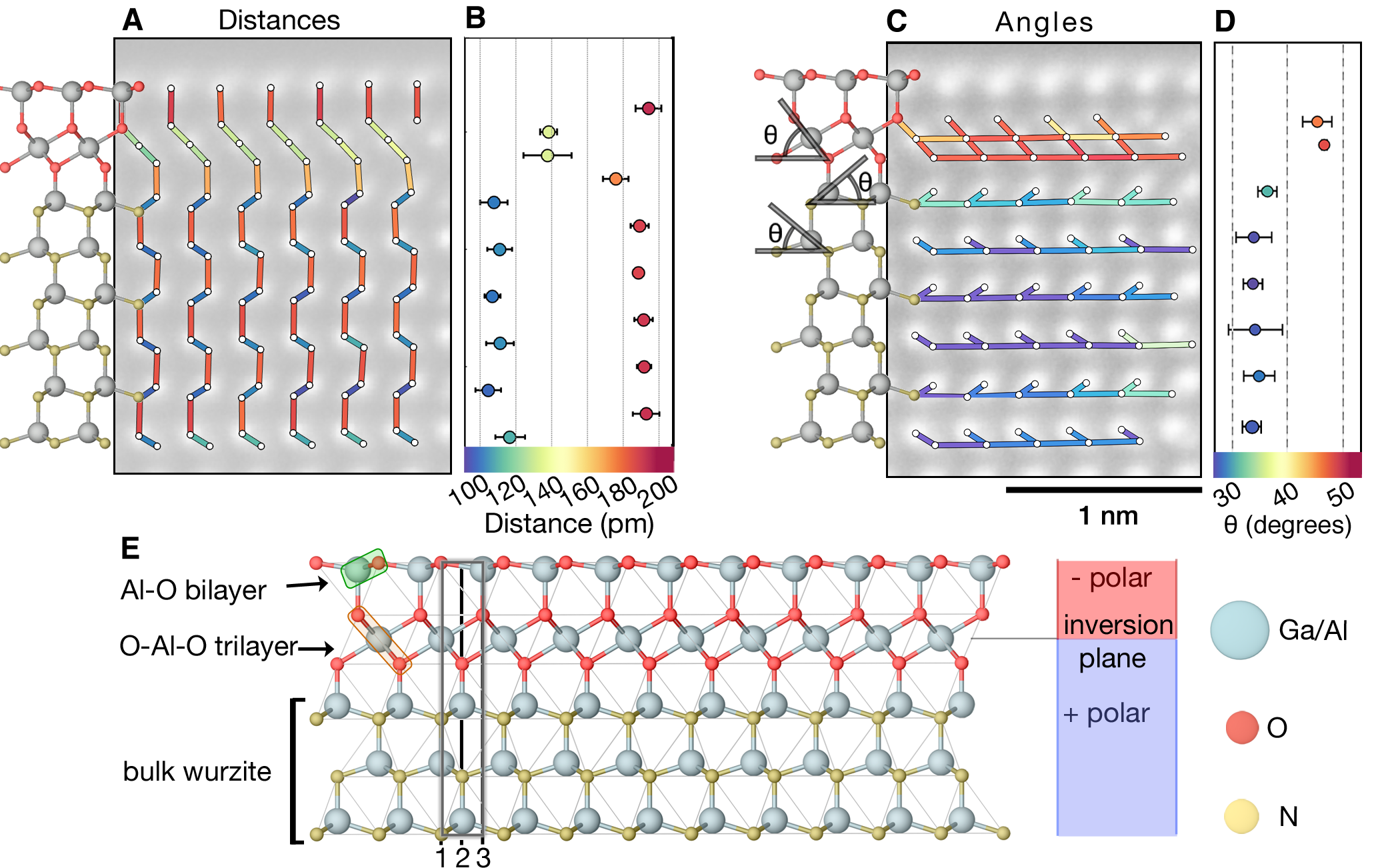
The model constructed from the structural measurements provides insights into atom coordination of the oxides. First, for both Ga and Al oxides, the last cation layer at the oxide/nitride interface remains tetrahedrally coordinated with N at the base and O at the apex of the tetrahedron. Second, highly distorted cation–O octahedra are observed at the central oxide layer. This configuration appears encouraged by the tetrahedral coordination at the c–plane surface. While this mixture of coordination is not present in the stable -Al2O3 phase (?, ?), the two-dimensional structure observed here is structurally similar to -Al2O3 and –Ga2O3, which both exhibit coexisting tetrahedral and octahedral cation coordination. It is also noted in Figure 3E that there is an inversion of polarity across the mid-plane of the oxide trilayer based on this configuration, which suggests a role of these surface oxides in compensating the strong, built–in polarization field of the wurtzite nitride.
Though the oxidized surfaces of GaN and AlN have been studied and modeled for some time, this direct observation of the surface with depth resolution reveals a new structure that differs from those previously investigated. To understand the energetic stability of this structure, we compare it with previously proposed models (?, ?) using DFT. In those works, it was found that the most energetically favorable structures consist of either an octahedrally coordinated O–III–O trilayer or a tetrahedrally coordinated III–O bilayer which can be seen at the top of Figure 4. An ideal version of the observed structure maintains the bulk oxide 2/3 cation-to-anion ratio. This is achieved by combining aspects of both trilayer and bilayer models, which was not previously considered.
The surface formation energy for each surface configuration is calculated via Equation 1. This surface energy is taken relative to a clean, smooth, and step-free cleaved nitride surface. Negative surface formation energies indicate that the oxidized configurations are favorable, for the particular set of conditions, relative to the unreconstructed and ideally flat surface. Absolute surface energies taken relative to the bulk are a challenge in this direction due to the lack of inversion symmetry along . Nevertheless, the relative energies provide insight into the favorability of one configuration as compared to another. The surface energy as a function of chemical potential is given by:
| (1) |
In this equation, is the total energy of the slab model containing the reconstruction, is the energy of the eight bilayer reference, is the area of the surface, is the number of atoms added to (positive) or removed from (negative) the surface structure with atoms being exchanged with a chemical reservoir described by the chemical potential , where is the element (Al, Ga, N, or O) being exchanged. The total chemical potential, , is , where is the reference chemical potential taken at 0 K and is the change in the chemical potential from that reference.
The calculated surface energies, , as a function of the Al and Ga chemical potential for the observed structure and previously proposed models, are presented in Figure 4. Based on an environment of air with an oxygen partial pressure of 0.2 atm at room temperature (298 K), is fixed at -0.3 eV (?). Of the previously reported structures, those consisting of an O–Al–O trilayer were shown to be more energetically stable. For the observed structure, is lower than all the previous models across the range of Al and Ga relevant chemical potentials.

Using the relaxed DFT model based on the observed structure, STEM image simulations, Figure S4, are in excellent agreement with the experiment. While the STEM images from experiment shows that the oxide exhibits a slightly lower overall intensity compared to simulations, this can be due either incomplete coverage of the oxide on the sample surface, differences in static and thermal atomic displacement factors, unoccupied cation sites, or a combination thereof. To further validate the surface oxide model, the bond lengths and angles are compared between experiment and DFT. The bond length measurements are shown in Table 1. The trends for each bond in and between the nitride and oxide are in excellent agreement. Quantitatively, the bond lengths exhibit at most 5% error. The largest deviation occurs at the oxide/nitride interface. Further, the agreement extends to the bond angles, matching experiment and theory to within 0.5∘.
Given the structure of the stable 2D oxides, there are a number of consequences. First, inversion domain boundaries are often found in thin film nitrides (?), and the observed oxides offer a mechanism for their creation. Notably, the oxides inherently reverse polarity through the transition from octahedral to tetrahedral bonding as discussed above. The inversion of polarity in the outer most layer of the oxide would seed N-polar nitride growth. Supporting this hypothesis, oxygen has been found at the initiation site of inverted domains, forming AlN1-xOx at elevated growth temperatures (?). Although the 2D oxide and the AlN1-xOx by Mohn et al. differ in structure, they consist of similar octahedral and tetrahedral bonding units. Differences between the two structures may result from reaction of the 2D oxide seed layer during subsequent high temperature growth.
The structure of the observed oxide also explains the results from a recent study growing ZnO grown epitaxially on GaN. In that case, the surface of the GaN was intentionally oxidized before ZnO growth, where the ZnO polarity was then inverted (?). The authors of that work hypothesized that a monolayer oxide was responsible for the polarity inversion and high quality of growth. The structural models provided here therefore provide critical insight into reducing defects as well as improved heteroepitaxial oxide–nitride thin film structures.
These 2D oxides appear similar to the recently reported formation of a 2D form of GaN (?). The structure, stabilized by encapsulation with graphene, also exhibits octahedral – tetrahedral bonding in a trilayer – bilayer configuration. In both cases, the polarity is inverted across the central trilayer, which could aid in charge compensation. As such, this structural configuration may be a hallmark of Ga- and Al- based 2D oxides and nitrides. Further, these similarities motivate future directions of research in the development of a mechanistic understanding of such 2D structures on polar surfaces and demonstrates that even though the nitrides have been studied for decades new discoveries remain.
In summary, by combining experiment and theory, we have the directly solved the structure of two-dimensional oxides forming natively on AlN and GaN surfaces. These oxide structures provide key observations to explain the formation of inversion domains and the origin of surface states that significantly influence the performance of III-nitride based devices. Further, these models offer direct evidence to model electronic surface states within the bulk band structure. Because of the relative ease of forming these structures, we also propose that such a platform may provide opportunities for exploring the properties and electronic behavior of two dimensional oxides not previously considered.
References
- 1. L. Bjaalie, B. Himmetoglu, L. Weston, A. Janotti, C. G. V. de Walle, New Journal of Physics 16, 025005 (2014).
- 2. G.-z. Zhu, G. Radtke, G. A. Botton, Nature 490, 384 (2012).
- 3. N. Shibata, et al., Science 322, 570 (2008).
- 4. W. Xu, J. Dycus, X. Sang, J. LeBeau, Ultramicroscopy 164, 51 (2016).
- 5. M. Shur, B. Gelmont, M. a. Khan, Journal of Electronic Materials 25, 777 (1996).
- 6. J. Z. Li, J. Y. Lin, H. X. Jiang, M. A. Khan, Q. Chen, Journal of Vacuum Science & Technology B 15, 1117 (1997).
- 7. B. Jogai, Journal of Applied Physics 93, 1631 (2003).
- 8. G. Koley, M. G. Spencer, Applied Physics Letters 86 (2005).
- 9. H. Liao, R. Sodhi, T. W. Coyle, Journal of Vacuum Science & Technology A: Vacuum, Surfaces, and Films 11, 2681 (1993).
- 10. V. M. Bermudez, Journal of Applied Physics 80, 1190 (1996).
- 11. R. Dalmau, R. Collazo, S. Mita, Z. Sitar, Journal of Electronic Materials 36, 414 (2007).
- 12. J. Li, et al., Journal of the American Ceramic Society 89, 937 (2006).
- 13. A. Rice, et al., Journal of Applied Physics 108, 043510 (2010).
- 14. J. A. Enterkin, et al., Nature Materials 9, 245 (2010).
- 15. Y. Dong, R. M. Feenstra, J. E. Northrup, Journal of Vacuum Science & Technology B: Microelectronics and Nanometer Structures 24, 2080 (2006).
- 16. M. S. Miao, J. R. Weber, C. G. Van de Walle, Journal of Applied Physics 107, 123713 (2010).
- 17. J. Houston Dycus, R. M. White, J. M. Pierce, R. Venkatasubramanian, J. M. LeBeau, Applied Physics Letters 102, 081601 (2013).
- 18. X. Sang, J. M. LeBeau, Ultramicroscopy 138, 28 (2014).
- 19. J. H. Dycus, et al., Microscopy and Microanalysis 21, 946 (2015).
- 20. J. Jones, Acta Crystallographica Section B: Structural Crystallography and Crystal Chemistry 24, 355 (1968).
- 21. R.-S. Zhou, R. L. Snyder, Acta Crystallographica Section B: Structural Science 47, 617 (1991).
- 22. M.-H. Lee, C.-F. Cheng, V. Heine, J. Klinowski, Chemical physics letters 265, 673 (1997).
- 23. W. G. Mallard, P. Linstrom, Gaithersburg, MD 20899 (2009).
- 24. S. Mohn, et al., Phys. Rev. Applied 5, 054004 (2016).
- 25. S. Mohn, et al., Physical Review Applied 5, 054004 (2016).
- 26. M. B. Ullah, et al., physica status solidi – Rapid Research Letters 10, 682 (2016).
- 27. Z. Y. Al Balushi, et al., Nature Materials (2016).
- 28. R. Dalmau, et al., Journal of The Electrochemical Society 158, H530 (2011).
- 29. S. Mita, R. Collazo, A. Rice, R. Dalmau, Z. Sitar, Journal of Applied Physics 104, 013521 (2008).
- 30. J. H. Dycus, J. M. LeBeau, J. Microsc. in press (2017).
- 31. P. Voyles, J. Grazul, D. Muller, Ultramicroscopy 96, 251 (2003). Proceedings of the International Workshop on Strategies and Advances in Atomic Level Spectroscopy and Analysis.
- 32. J. M. LeBeau, S. D. Findlay, L. J. Allen, S. Stemmer, Ultramicroscopy 110, 118 (2010).
- 33. X. Sang, A. A. Oni, J. M. LeBeau, Microscopy and Microanalysis 20, 1764 (2014).
- 34. E. J. Kirkland, Advanced Computing in Electron Microscopy (Springer, New York, 2010), second edn.
- 35. G. Kresse, J. Hafner, Physical Review B 47, 558 (1993).
- 36. G. Kresse, J. Hafner, Phys. Rev. B 49, 14251 (1994).
- 37. G. Kresse, J. Furthmüller, Computational materials science 6, 15 (1996).
- 38. G. Kresse, J. Furthmüller, Phys. Rev. B 54, 11169 (1996).
- 39. J. P. Perdew, K. Burke, M. Ernzerhof, Phys. Rev. Lett. 78, 1396 (1997).
Acknowledgements
JML, JHD, and EDG gratefully acknowledge support for this research from the Air Force Office of Scientific Research (Grant No. FA9550-14-1-0182). DLI and KJM acknowledge financial support from the NSF under grant DMR-1151568. JHD and EDG acknowledge support by the National Science Foundation Graduate Research Fellowship (DGE-1252376). R.K., S.M., R.C., and Z.S. sincerely thank support from NSF (ECCS-1508854, ECCS-1610992, DMR-1508191, ECCS-1653383), and the Army Research Office (W911NF-15-2-0068, W911NF-16-C-0101) for funding. This work was performed in part at the Analytical Instrumentation Facility (AIF) at North Carolina State University, which is supported by the State of North Carolina and the National Science Foundation (ECCS-1542015). AIF is a member of the North Carolina Research Triangle Nanotechnology Network (RTNN), a site in the National Nanotechnology Coordinated Infrastructure (NNCI).
Author Contributions
J.H.D and J.M.L designed the experiments and carried out the STEM imaging and subsequent image analysis. K.J.M. and D.L.I performed the DFT calculations and analysis. E.D.G performed the multislice STEM image simulations of the structural model. R.K., S.M., R.C., and Z.S. performed the sample growth. J.M.L., D.L.I., R.C., and Z.S. supervised the research. All authors contributed to discussions and preparation of the manuscript.
Supplementary materials
Materials and Methods
Figures S1 to S4
Table S1
References (30-39)
Supplementary Materials for: Structure of Native Two-dimensional Oxides on III–Nitride Surfaces
Materials & Methods
Experiment
Thin film AlN and GaN samples were prepared by MOCVD growth following methods described in Ref. (?, ?). Thin film cross sections were prepared for TEM using the methods described in Refs. (?) and (?). Subsequent to mechanical polishing, samples were prepared with and without Ar ion milling to determine the impact of the milling process. For this step, a Fischione 1050 TEM mill was for final thinning at 1.0 keV and 0.4 keV for 10 minutes and 20 minutes respectively. It is noted that the same structure is observed for samples that were prepared with and without ion milling. Similarly, the samples were imaged with and without plasma cleaning, and the same surface structure was observed under both conditions. To remove any damaged surface layer during sample preparation, a dilute 5% HF solution was used to etch the TEM samples for one minute. It is noted that the same structure is observed for each variation of the preparation step.
A FEI Titan G2 60–300 kV TEM/STEM was operated at 200 keV for spectroscopy and 300 keV for imaging. For AlN, the annular dark-field collection range was 34-208 mrad at 200 keV and 30-185 mrad at 300 keV. The probe–forming convergence semi-angle was 19.6 mrad in each case. For GaN, the annular dark-field collection range was 22 mrad and 134 mrad at 200 keV and 19 mrad and 118 mrad at 300 keV. To minimize beam damage, the probe current was kept below 30 pA. Sample thicknesses were approximately 5 nm as determined by position averaged convergent beam electron diffraction (?)
To improve signal to noise and remove sample drift distortion, the RevSTEM method was used (?). Image series were acquired with at least 20 10241024 pixel frames at a pixel dwell time of 3 s/pixel with a 90 ∘ rotation between each frame. Atom column positions were fit to a two-dimensional Gaussian distribution with sub–pixel precision and indexed into a matrix (?). The pixel size was calibrated as described in Ref. (?). EELS maps were acquired using a Gatan Enfinium spectrometer. The O and N maps were extracted individually after fitting and subtracting the spectral background via fitting to a power law. Image simulations were carried out using the multislice method (?) with parameters taken from experiment. Thermal scattering was included with the frozen phonon approach and thermal displacements approximated by their bulk values.
Simulation and calculation details
DFT plane wave pseudopotential calculations, as implemented in the Vienna ab–initio Simulation Package (VASP) (?, ?, ?, ?), were used to determine surface formation energies. The gradient corrected Perdew-Burke-Enzerhof (PBE) (?) functional was used to handle exchange and correlation contributions to the total energy. Projector augmented pseudopotentials for Al, Ga, N,and O contained 3, 13, 5, and 6 valence electrons, respectively. A kinetic energy cutoff of 520 eV was used for all structures. Each oxide was oriented along a cleaved and unreconstructed (0001) plane of the wurtzite AlN/GaN structure that consisted of eight bilayers. A 20 Å vacuum padding was also included to minimize surface-surface interactions between both sides of the slab. Exposed N atoms at bottom of the slab were passivated with partially charged H (charge equal to 0.75) to remove surface states and prevent charge transfer between both surfaces of the slab.
Supporting Figures


.

![[Uncaptioned image]](/html/1708.03997/assets/figures/STEMvsDFT.png)