Interband -like plasmon in silicene grown on silver
Abstract
Silicene, the two-dimensional allotrope of silicon, is predicted to exist in a low-buckled honeycomb lattice, characterized by semimetallic electronic bands with graphenelike energy-momentum dispersions around the Fermi level (represented by touching Dirac cones). Single layers of silicene are mostly synthesized by depositing silicon on top of silver, where, however, the different phases observed to date are so strongly hybridized with the substrate that not only the Dirac cones, but also the whole valence and conduction states of ideal silicene appear to be lost. Here, we provide evidence that at least part of this semimetallic behavior is preserved by the coexistence of more silicene phases, epitaxially grown on Ag(111). In particular, we combine electron energy loss spectroscopy and time-dependent density functional theory to characterize the low-energy plasmon of a multiphase-silicene/Ag(111) sample, prepared at controlled silicon coverage and growth temperature. We find that this mode survives the interaction with the substrate, being perfectly matched with the -like plasmon of ideal silicene. We therefore suggest that the weakened interaction of multiphase silicene with the substrate may provide a unique platform with the potential to develop novel applications based on two-dimensional silicon systems.
pacs:
73.20.Mf,73.22.Lp,73.22.PrI introduction
Following the isolation of graphene sheets by mechanical exfoliation of its parent crystal graphite 1 , enormous effort has been directed towards two-dimensional (2D) crystals made of group-IV elements other than carbon.
A particularly noteworthy example is silicene, the silicon equivalent of graphene with a natural compatibility with current semiconductor technology 7 ; 7b ; 7c . First-principles calculations of the structural properties report an intrinsic stability of a honeycomb arrangement of Si atoms in slightly buckled form, with mixed - hybridization 2 ; 3 ; 4 . This system, referred to as freestanding or silicene, presents a graphenelike, semimetallic electronic structure characterized by linearly dispersing and bands around the Fermi energy , thus effectively allowing the charge carriers to mimic massless relativistic particles 8 ; 9 . Unlike graphene, freestanding silicene has a large spin-orbit coupling, which would make it suitable for valley-spintronic applications 10 ; 10b , and an electrically, magnetically, or chemically tunable band gap 11a ; 11b ; 11 ; 11c ; 11d ; 11e , which would be crucial for engineering on-off current ratios and charge-carrier mobility in silicene field-effect transistors.
On the practical side, silicenelike nanostructures are synthesized by the epitaxial growth 14 ; 13b of silicon on silver 12 ; 6b ; 13 ; 14cc ; 5 ; 6 ; 6c and a few other metal substrates 14b ; 14c , very recently including gold 47 . In particular, a number of well-ordered domains have been observed on Ag(111), the formation and coexistence of which depend on the substrate temperature, during silicon growth, and the silicon deposition rate 15 ; 16 ; 17 ; 17bb ; 17ccc ; 18 ; 23 .
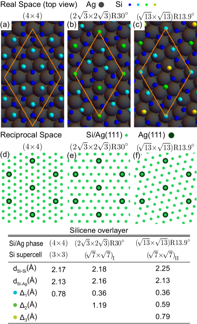
Most of these domains have a crystalline morphology that is closely commensurate with the , , and phases 17bb ; 18 ; 23 ; 20 ; 21 ; 24 ; 26 ; 26BB ; 26CC ; 26dd ; 26eeex ; 26eeey ; 22 of Fig. 1. The different orientation, out-of-plane atomic buckling, and lattice constant of the Si atoms in these superstructures, here denoted , , and , are refected in markedly distinct electronic properties of the silicene overlayers that, even without the supporting Ag substrate below, may or may not preserve the Dirac cones of silicene 17ccc ; 17bb ; 27 ; 28 . Other phases and more complex scenarios, including silicon-induced faceting, are reported in the literature 6c ; 20 ; 17ccc ; 27 ; 28yyy ; 28xxx .
As for the interaction with Ag(111), silicene seems to lose the unique properties of its form, as confrmed by angle-resolved photoemission spectroscopy (ARPES) measurements combined with density functional calculations 25 ; 19 ; 25bb ; 29 ; 30 ; 31 . Indeed, the initial evidence of Dirac cones in the phase 6 ; 23 has been reinterpreted as originating from the s and p states of bulk Ag, or the strongly hybridized sp states of Ag and Si 31 . More recent developments 32 suggest that a hybridized Dirac-cone structure is unusually formed, as a result of the aforementioned hybridization. Even in this latter case, however, the -like bands of freestanding silicene are destroyed by its interaction with Ag. Thus, contrary to well-consolidated technologies of graphene growth on copper, the transfer of silicene to other substrates appears impractical.
The intercalation of alkali-metal atoms between silicene and Ag(111) is predicted to effectively restore the Dirac cones 32b . Another possibility has been indicated by changing the supporting substrate to Au(111) 47 . Nonetheless, the major goal of silicene technology is still to grow a honeycomblike structure of Si atoms with semimetallic, -like electronic features.
A different possible direction is outlined here, where, rather than looking at the band structure of silicene on Ag(111), we consider exploring the intrinsic plasmonics of the interface, i.e., the coherent charge-density oscillations of its valence electrons (plasmons). Specifically, we present low-energy electron diffraction (LEED) and electron energy loss spectroscopy (EELS) characterizations of two surface reconstructions of silicene on Ag(111), being, respectively, given by the and a mixture of the , , and superstructures (Sec. II). We report a clear signature of the existence of and states of silicene in the mixed phase, which reflects in a -like plasmon structure detected in the energy loss (EL) spectrum of the system, alongside the Ag plasmon (Sec. II).
The measurements are consistent with time-dependent (TD) density functional theory (DFT) (TDDFT) calculations of the EL function of silicene 33 , showing a well-resolved loss peak at 1.75 eV for a momentum transfer of the order of 10-2 Å-1 (Sec. III). Furthermore, our results indicate that at least part of the or character of the first valence band (VB) or first conduction band (CB) of silicene grown on Ag(111) may be maintained under specific geometric conditions (Sec. III). On the other hand, the -like mode is absent in each single pure phase of the above-mentioned types, thus confirming that the semimetallic character of freestanding silicene is lost in favor of a hybridized band structure (Sec. IV).
II Preparation and characterization of the samples
To begin, the experiments were carried out at room temperature in an ultrahigh vacuum chamber (with a base pressure of 210-10 Torr), using a high-resolution electron energy loss (EEL) spectrometer, equipped with two 50-mm hemispherical defectors, as both monochromator and analyzer.
The EL spectra were acquired with an incident electron beam, about 0.2 mm wide, positioned at a fixed angle of 45∘ from the surface normal. The kinetic energy of the incident electrons was 40 eV. Scattered electrons were collected at an angle of 46∘ from the surface normal, with an overall energy resolution of 20 meV and an angular acceptance of 2∘.
The silver substrate (a disk of about 8 mm diameter) was cleaned through several cycles of sputtering with 1 keV Ar+ ions, at an operating pressure of 510 Torr, followed by annealing at 500∘C until a sharp LEED pattern showed the achievement of a clean and well-ordered Ag(111) surface.
Silicon was deposited on Ag(111) by thermal evaporation from a pure source, which was slab cut from a silicon wafer, clamped between two electrodes, and heated up, by passing a direct current thorough it, to obtain a stable vapor flux. During deposition, the silicon source was placed in front of the silver substrate, which was maintained at a constant temperature, controlled by a thermocouple placed close to the sample. The pressure during growth was less than 210 Torr. The uptake of Si was monitored by x-ray photoelectron spectroscopy and LEED.
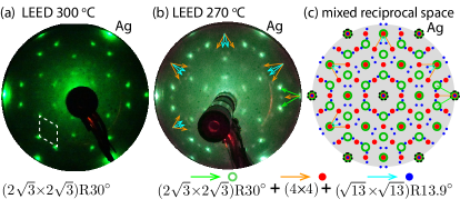
Figure 2(a) shows the diffraction pattern acquired with the Ag substrate kept at 300∘C, during Si deposition. The LEED spots from this first sample are consistent with the reciprocal space points of Fig. 1(e), also reported in Fig. 2(c). Accordingly, they are readily interpreted as originating from a sufficiently pure phase, in agreement with several previous studies 15 ; 16 ; 26BB ; 26CC ; 26eeex . On the other hand, the LEED image of Fig. 2(b) was acquired with the Ag substrate kept at 270∘C, during Si deposition.
This second sample is characterized by a mixture of the ,, and phases, confirming that the growth conditions are very sensitive to the substrate temperature 16 ; 17 ; 17ccc . The possible formation of recently isolated multilayer silicene can be ruled out, because it would provide a different LEED pattern 25 .
Indeed, the LEED spots from the second sample are in line with the reciprocal space points of the three phases, reported in Fig. 2(c), where the silicene superstructures are assumed to be perfectly matched with the Ag substrate. Interestingly, a visual inspection of Figs. 2(b) and 2(c) suggests a lattice mismatch of the and overlayers of 1 and 5, respectively. Similar patterns, mostly concerning the andphases, have been discussed elsewhere 14 ; 15 ; 26eeex ; 26eeey ; 26dd , nonetheless, our composite structure, presenting a dominant phase, which coexists with the andphases has yet to be reported.
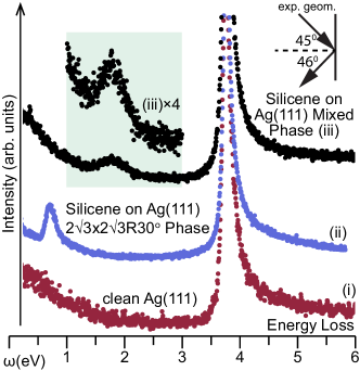
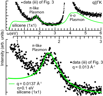
The EELS measurements were performed with the samples directly transferred in the ELL spectrometer, without breaking the vacuum, and kept at room temperature with a pressure below 210-10 Torr. Figure 3 shows the EL spectra, in the range of 0-6 eV, obtained from (i) clean Ag(111), (ii) the pure phase with the LEED pattern of Fig. 2(a), and (iii) the mixed phase with the LEED pattern of Fig. 2(b).
A prominent feature at 3.8 eV, which corresponds to the surface plasmon of Ag(111), dominates all spectra. Besides, the Si/Ag(111) spectrum shows an additional loss at 0.7eV in the pure phase and 1.75 eV in the mixed phase. The excitation energy of the former mode suggests the presence of a hybridized Si-Ag plasmon, whereas the latter mode resembles the -like plasmon of silicene 33 .
III Intrinsic plasmonics of the silicene systems
To support the unprecedented observation outlined in the previous section, we used TDDFT in the random phase approximation (RPA) and computed the dielectric properties of silicene 33 in comparison with the , , and overlayers of silicene, peeled from the silver substrate, in the , , and phases of Fig. 1. These superstructures represent instructive examples of monolayer silicene, which, without the Ag substrate below, would not [Fig. 4(a)] and would [Fig. 4(b) and 4(c)] preserve the Dirac-cone features 17ccc ; 17bb ; 27 ; 28 .
As it is customary in TDDFT 34 , we started with a calculation of the ground-state electronic properties of the silicene systems by DFT 35 in the Kohn-Sham (KS) approach 37 , using the generalized gradient approximation (GGA) 36a and eliminating the core electrons by suitable norm-conserving pseudo-potentials 38 . We selected a plane-wave (PW) basis set, within an energy cutoff of 25 hartree, to represent the KS electron states , associated with the band energies , being labeled by a band index and a wave vector in the first Brillouin zone (). The bulk-geometry, inherent to PW-DFT, was generated by replicating the silicene slabs with an out-of-plane vacuum distance of Å.
Geometry optimization was performed on unsupported silicene, obtaining a lattice constant of and a characteristic buckling of the AB type, specified by a buckling distance of 33 .
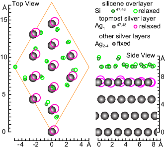
As for supported silicene, the substrate was simulated by four silver planes with the morphologies of Fig. 1, starting from a set of optimized parameters found in Refs. 27 ; 28 . Then, the positions of all atoms in the silicene and topmost Ag layers were relaxed using a Monkhorst-Pack (MP) grid 39 of in the , with the occupied and the first few empty band-states of the systems. Further details on the electronic features of the phase are provided in Sec. S1 of the Supplemental Material supX .
Single-point self-consistent runs were carried out in the local density approximation (LDA) 36 on a finer MP mesh of , by removing the silver layers and keeping the same optimized positions for the Si atoms as the geometry optimization step. Subsequently, the converged electron densities were used, in non-self-consistent runs, to obtain the eigensystem on highly resolved grids of points, for silicene, points, for silicene, and points for the other two silicene superstructures [ and ]. A number of empty bands covering the KS energy spectrum up to 15 eV, above , was selected in all non-self-consistent cases, to accurately describe the systems’ plasmonics at energy losses below 6 eV.
The electronic structure and density of states (DOS) of our DFT+LDA computations are reported in Fig. 4, with the band energies represented along the paths of the corresponding reciprocal spaces (Fig. 1). Here, we spot some peculiar features partly recognized in previous studies 27 ; 28 ; 33 . silicene has no Dirac cones at K and presents a direct gap at of eV, between two couples of nearly degenerate states of leading and symmetries, respectively [Fig. 4(a)]. , and silicene exhibit a quasilinear -like dispersion in the first VB and first CB at , i.e., a Dirac-cone structure with a tiny band gap below [Fig. 4(b), (c)]. The second VB and CB of these superstructures are of dominant symmetry. silicene has two quasimetallic bands of dominant character [Fig. 4(d)], whose dispersions resemble the bands of graphene 33xx on a reduced energy scale and with a smaller Fermi velocity 33 . Even in the latter case, the second VB and CB are dominantly , however, a inversion has been detected at the crossing points between the first and second VBs and the (avoided) crossing points between the first and second CBs 33 .
All these silicene systems have specific high intensity peaks in the DOS that support electron excitations between the first or second VB and CB near , in a region of the where the bands are quasiflat, and may assist -like and - plasmon oscillations. The corresponding low-energy vertical transitions, which lead to small-momentum EL-peaks, are indicated by dashed arrow lines in Figs. 4 and 5.

As a second step of the TDDFT framework, we computed the unperturbed susceptibility of the KS electrons to an energy loss and momentum transfer from the incident electron, provided by 40
| (1) |
The latter (reported in Hartree atomic units) includes a factor of 2 for the electron spin, the Fermi-Dirac occupations and (evaluated at room temperature), a lifetime broadening parameter (set to ), and the density-density correlation matrix elements .
The full susceptibility was obtained using the central equation of TDDFT 42 :
| (2) |
Working the RPA, we represented the interaction matrix elements in by a truncated Coulomb potential, which has been accurately designed to exclude the unphysical interaction between the silicene slab replicas in a broad range of transferred momenta across the whole 43 ; 44 ; 45 .
Accordingly, the inverse permittivity was obtained as and the EL function was calculated from the macroscopic average . Nonlocal field effects 46 were included in through a dimensional cut-off on the central equation of TDDFT, which we verified to converge by reduction to a matrix equation, including the smallest vectors sorted in length from .
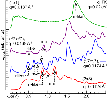
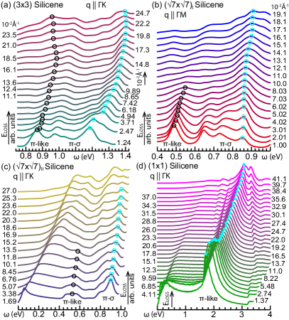
In Fig. 5, we compare the theoretical loss spectra of our silicene systems, at fixed small momentum transfers parallel to in an energy loss range below . The superstructures present a sequence of low-energy peaks associated with quasivertical electron excitations between the first or second VB and CB, of dominant or character, given in Fig. 4(a)-(c). Accordingly, the momentum-dependent investigation of Fig. 6(a)-(c) let us identify two dispersive modes, which we respectively attribute to a -like plasmon, assisted by first-VB-to-first-CB transitions, and a - plasmon, assisted by second-VB-to-first-CB and first-VB-to-second-CB transitions. Much insight into the latter oscillation in silicene is provided in Sec. S2 of the Supplemental Material supX .
More importantly, we notice that there is no way that the EL functions of the silicene superstructures can be combined to reproduce the experimental loss spectrum of the mixed phase [curve (iii) in Fig. 3]. On the contrary, silicene exhibits a broad primary -like plasmon peak [Figs. 5 and 6(d)], consistent with the EELS spectrum of the mixed phase, which is assisted by first-VB-to-first-CB transitions around the M-point and superimposed to secondary one-electron excitation structures. The detailed features of this mode have been carefully addressed in in Ref. 33 , and are briefly recalled in Sec. S3 of the Supplemental Material supX . A - mode is also present at energies larger than eV (Fig 7).
IV Loss-peak of the mixed phase and -like plasmon of silicene
Of particular significance, in the loss function analysis presented so far, are the low energy features at eV, for silicene, and eV, for , silicene, because they appear not to be completely erased by the interaction with Ag(111).
Indeed, the experimental loss of the pure phase [spectrum (ii) in Fig. 3] shows a peak, which has some match with the low-energy end of the theoretical loss function of silicene, lying within the energy window of vertical transitions associated with the - plasmon (Figs. 4 and 5).
The interaction with silver destroys the high-energy loss properties of the peeled phase and distorts the low-energy peak, which we ascribe to a hybridized Si-Ag plasmon. This interpretation is confirmed by existing DFT calculations 31 and validated by our analysis on the phase in Secs. S1 and S2 of the Supplemental Material supX , suggesting that the low-energy mode arises due to charge-density oscillations within the silicene and first silver layer and keeps trace of the peeled phase (Figs. F2 and F5 in the Supplemental Material supX ). On the contrary, no signature of an interband plasmon at appears in the theoretical loss spectrum of the silicene superstructures.
A more suggestive result is shown in Fig. 7, where silicene calculations are compared with the EL measurements on the coexisting silicene/Ag(111) phases [loss-curve (iii) in Fig. 3]. The excellent agreement, at energy losses below , lets us conclude that this morphology indeed presents a dielectric response that matches what is expected for the -like plasmon of ideal silicene. Also interesting to notice is that the plasmon of silicene may be present as well, though it is hidden by the Ag plasmon of the interface, as verified by comparing the loss spectrum of the mixed phase with that of clean Ag(111) [(i) in Fig. 3].
Hence, the interaction between the pure phases not only weakens the hybridization of Si and Ag states, but also appears to merge the different buckling levels of supported silicene into a configuration that resembles that of freestanding silicene. Indeed, the different silicene superstructures are expected to arrange into buckling conformations that mimic that of silicene, when their distances relative to the Ag substrate are increased above the Å values, predicted for the pure phases. Our DFT calculations on the phase indicate that the silicene domains begin to form for average Si-Ag distances larger than Å [see Fig. F3 in Sec. S1 of the Supplemental Material supX ]. This is the main result of the present study, which awaits further scrutiny, especially regarding the dispersion of the newly discovered -like mode [see Appendix S3 of the Supplemental Material supX ].
V Conclusions
To summarize our results, we have presented a combined experimental (EELS) and theoretical (TDDFT) approach to show that silicene grown in a mixed phase on Ag(111) preserves at least part of the semimetallic character of its freestanding form, exhibiting an interband -like plasmon assisted by excitation processes at the M-point of the . Such a mode parallels the plasmon of freestanding graphene 33 . The presence of a -like plasmon by itself does not allow us to conclude that the silicene overlayer maintains its natural Dirac-cone structure. For example, the interfaces of graphene on the (111) faces of copper and nickel have a well-characterized , with the Dirac cone being preserved and destroyed, respectively, by hybridization with the bands of the supporting metal 33aa ; 33bb . Nevertheless, in the latter case the shape, position and dispersion of the plasmon peak is substantially different from that of freestanding graphene 33cc , which encourages performing further investigations on mixed-phase morphologies of silicene on silver. A similar approach would help to characterize the first VB and CB of Silicene on Au(111) 47 , and corroborate the expected Dirac cone properties of the system.
On the other hand, recent progress on the epitaxial synthesis of pure, single phases of silicene on Ag(111), supported by DFT computations of their electronic properties, indicate that strong hybridization effects make it impractical to separate a silicene structure with a well-defined quasimetallic character. An experimental fingerprint of this phenomenon is the hybridized Si-Ag plasmon, discovered at low energy. Our proposal is then to shift the efforts of making silicene a feasible two-dimensional nanomaterial beyond graphene on the epitaxial growth of silicene in mixed domains.
Acknoledgements
A. S. acknowledges the computing facilities provided by the CINECA Consortium, within the INF16_npqcd project, under the CINECA-INFN agreement, and the IsC49_PPGRBGI project.
References
- (1) K. S. Novoselov, A. K. Geim, S. V. Morozov, D. Jiang, Y. Zhang, S. V. Dubonos, I. V. Grigorieva, and A. A. Firsov, Electric Field Effect in Atomically Thin Carbon Films,i Science 306, 666 (2004)
- (2) A. Kara, H. Enriquez, A.P. Seitsonen, L. C. Lew Y. Voon, S. Vizzini, B. Aufray, and H. Oughaddou, A review on silicene–New candidate for electronics, Surf. Sci. Rep. 67, 1 (2012)
- (3) M. Houssa, A. Dimoulas, A. Molle, Silicene: a review of recent experimental and theoretical investigations, J. Phys.: Condens. Matter 27, 253002 (2015)
- (4) S. Cahangirov, H. Sahin, G. Le Lay, A. Rubio, Introduction to the Physics of Silicene and other 2D Materials, Lecture Notes in Physics, No. 930 (Springer, Berlin, 2017)
- (5) K. Takeda and K. Shiraishi, Theoretical possibility of stage corrugation in Si and Ge analogs of graphite, Phys. Rev. B 50, 14916 (1994)
- (6) G. G. Guzman-Verri and L. C. Lew Yan Voon, Electronic structure of silicon-based nanostructures, Phys. Rev. B 76, 075131 (2007)
- (7) S. Cahangirov, M. Topsakal, E. Akturk, H. Sahin, and S. Ciraci, Two- and one-dimensional honeycomb structures of silicon and germanium, Phys. Rev. Lett. 102, 236804 (2009)
- (8) S. Lebègue, O. Eriksson, Electronic structure of two-dimensional crystals from ab initio theory, Phys. Rev. B 79, 115409 (2009)
- (9) L. C. Lew Yan Voon, E. Sandberg, R.S. Aga, A.A. Farajian, Hydrogen compounds of group-IV nanosheets, Appl. Phys. Lett. 97, 163114 (2010)
- (10) C.-C. Liu, W. Feng, Y. Yao, Quantum Spin Hall Effect in Silicene and Two-Dimensional Germanium, Phys. Rev. Lett. 107, 076802 (2011)
- (11) H. Pan, Z. Li, C.-C. Liu, G. Zhu, Z. Qiao, and Y. Yao, Phys. Rev. Lett. 112, 106802 (2014)
- (12) Z. Ni, Q. Liu, K. Tang, J. Zheng, J. Zhou, R. Qin, Z. Gao, D. Yu, J. Lu, Tunable bandgap in silicene and germanene, Nano Lett. 12, 113 (2011)
- (13) T. H. Osborn, A. A. Farajian, O. V. Pupysheva, R. S. Aga, and L. L. Y. Voon, Ab initio simulations of silicene hydrogenation, Chem. Phys. Lett. 511, 101 (2011)
- (14) N. D. Drummond, V. Zólyomi, V. I. Fal’ko, Electrically tunable band gap in silicene, Phys. Rev. B, 85, 075423 (2012)
- (15) H.-R. Chang, J. Zhou, H. Zhang, and Y. Yao, Probing the topological phase transition via density oscillations in silicene and germanene, Phys. Rev. B 89, 201411 (2014)
- (16) C. J. Tabert and E. J. Nicol, Dynamical polarization function, plasmons, and screening in silicene and other buckled honeycomb lattices, Phys. Rev. B 89, 195410 (2014)
- (17) S. Trivedi, A. Srivastava, and R. Kurchania, Silicene and Germanene: A First Principle Study of Electronic Structure and Effect of Hydrogenation-Passivation, J. Comput. Theor. Nanosci. 11, 781 (2014)
- (18) B. Lalmi, H. Oughaddou, H. Enriquez, A. Kara, S. Vizzini, B. Ealet, and B. Aufray, Epitaxial growth of a silicene sheet, Appl. Phys. Lett. 97, 223109 (2010)
- (19) A. Bhattacharya, S. Bhattacharya, G. P. Das, Exploring semiconductor substrates for silicene epitaxy, Appl. Phys. Lett. 103, 123113 (2013)
- (20) C. Léandri, H. Oughaddou, B. Aufray, J.M. Gay, G. Le Lay, A. Ranguis, Y. Garreau, Growth of Si nanostructures on Ag(001), Surf. Sci. 601, 262 (2007)
- (21) A. Kara, C. Léandri, M. E. Dévila, P. De Padova, B. Ealet, H. Oughaddou, B. Aufray, G. Le Lay, Physics of Silicene Stripes, J. Supercond. Novel Magn. 22, 259 (2009)
- (22) B. Aufray, A. Kara, S. Vizzini, H. Oughaddou, C. Léandri, B. Ealet, and G. Le Lay, Graphene-like silicon nanoribbons on Ag(110): A possible formation of silicene, Appl. Phys. Lett. 96, 183102 (2010)
- (23) P. De Padova, C. Quaresima, C. Ottaviani, P. M. Sheverdyaeva, P. Moras, C. Carbone, D. Topwal, B. Olivieri, A. Kara, H. Oughaddou, B. Aufray, G. Le Lay, Evidence of graphene-like electronic signature in silicene nanoribbons, Appl. Phys. Lett. 96, 261905 (2010)
- (24) P. De Padova, P. Perfetti, B. Olivieri, C. Quaresima, C. Ottaviani, and G. Le Lay, 1D graphene-like silicon systems: silicene nano-ribbons, J. Phys.: Condens. Matter 24, 223001 (2012)
- (25) P. Vogt, P. De Padova, C. Quaresima, J. Avila, E. Frantzeskakis, M. C. Asensio, A. Resta, B. Ealet, and G. Le Lay, Silicene: compelling experimental evidence for graphenelike two-dimensional silicon, Phys. Rev. Lett. 108, 155501 (2012)
- (26) B. Feng, Z. Ding, S. Meng, Yugui Yao, X. He, P. Cheng, L. Chen, and K. Wu, Evidence of Silicene in Honeycomb Structures of Silicon on Ag(111), Nano Lett. 12, 3507 (2012)
- (27) A. Fleurence, R. Friedlein, T. Ozaki, H. Kawai, Y. Wang and Y. Yamada-Takamura, Experimental Evidence for Epitaxial Silicene on Diboride Thin Films, Phys. Rev. Lett. 108 245501 (2012)
- (28) L. Meng, Y. Wang, L. Zhang, S. Du, R. Wu, L. Li, Y. Zhang, G. Li, H. Zhou, W. A. Hofer, M. J. Gao, Buckled Silicene Formation on Ir(111), Nano Lett. 13 685 (2013)
- (29) S. Sadeddine, H. Enriquez, A. Bendounan, P. K. Das, I. Vobornik, A. Kara, A. J. Mayne, F. Sirotti, G. Dujardin, H. Oughaddou, Compelling experimental evidence of a Dirac cone in the electronic structure of a 2D Silicon layer, Sci. Rep. 7, 44400 (2017)
- (30) C.-L. Lin, R. Arafune, K. Kawahara, N. Tsukahara, E. Minamitani, Y. Kim, N. Takagi, and M. Kawai, Structure of Silicene Grown on Ag(111), Appl. Phys. Expr. 5, 45802 (2012)
- (31) H. Jamgotchian, Y. Colignon, N. Hamzaoui, B. Ealet, J.Y. Hoarau, B. Aufray, and J.P. Biberian, Growth of silicene layers on Ag(111): unexpected effect of the substrate temperature, J. Phys.: Condens. Matter 24, 172001 (2012)
- (32) Z. Majzik, M.R. Tchalala, M. Svec, P. Hapala, H. Enriquez, A. Kara, A.J. Mayne, G. Dujardin, P. Jelinek, and H. Oughaddou, Combined AFM and STM measurements of a silicene sheet grown on the Ag(111) surface, J. Phys.: Condens. Matter 25, 225301 (2013); H. Liu, J. Gao, J. Zhao, Silicene on substrates: interaction mechanism and growth behavior, J. Phys.: Conf. Ser. 491, 012007 (2014)
- (33) C. Grazianettia, D. Chiappe, E. Cinquanta, G. Tallarida, M. Fanciullia, A. Molle, Exploring the morphological and electronic properties of silicene superstructures, Appl. Surf. Sci., 291 109 (2014); Z. L. Liu, M. X. Wang, J. P. Xu, J. F. Ge, G. Le Lay, P. Vogt, D. Qian, C. L. Gao, C. H. Liu and J. F. Jia, Various atomic structures of monolayer silicene fabricated on Ag(111), New J. Phys, 16 075006 (2014)
- (34) E. Scalise, E. Cinquanta, M. Houssa, B. van den Broek, D. Chiappe, C. Grazianetti, G. Pourtoisc, B. Ealet, A. Molle, M. Fanciulli, V.V. Afanas’ev, A. Stesmans, Vibrational properties of epitaxial silicene layers on (111) Ag, Appl. Surf. Sci. 291, 113 (2014)
- (35) P. Moras, T.O. Mentes, P.M. Sheverdyaeva, A. Locatelli, and C. Carbone, Coexistence of multiple silicene phases in silicon grown on Ag(111), J. Phys.: Condens. Matter 26, 185001 (2014)
- (36) H. Enriquez, S. Vizzini, A. Kara, B. Lalmi, and H. Oughaddou, Silicene structures on silver surfaces, J. Phys.: Condens. Matter 24, 314211 (2012)
- (37) R. Arafune, C.-L. Lin, K. Kawahara, M. Kanno, N. Tsukahara, E. Minamitani, Y. Kim, N. Takagi, and M. Kawai, Structural transition of silicene on Ag(111), Surf. Sci. 608, 297 (2013)
- (38) K. Kawahara, T. Shirasawa, R. Arafune, C.-L. Lin, T. Takahashi, M. Kawai, and N. Takagi, Determination of atomic positions in silicene on Ag(111) by low-energy electron diffraction, Surf. Sci. 623, 25 (2014)
- (39) M.R. Tchalala, H. Enriquez, H. Yildirim, A. Kara, A.J. Mayne, G. Dujardin, M. Ait Ali, and H. Oughaddou, Atomic and electronic structures of the ()R13.9∘ of silicene sheet on Ag(111), Appl. Surf. Sci. 303, 61 (2014)
- (40) C.-L. Lin, R. Arafune, K. Kawahara, M. Kanno, N. Tsukahara, E. Minamitani, Y. Kim, M. Kawai, and N. Takagi, Substrate-Induced Symmetry Breaking in Silicene, Phys. Rev. Lett. 110, 076801 (2013)
- (41) Z.-L. Liu, M.-X. Wang, C. Liu, J.-F. Jia, P. Vogt, C. Quaresima, C. Ottaviani, B. Olivieri, P. De Padova, and G. Le Lay, The fate of the silicene phase on Ag(111), APL Mater. 2, 092513 (2014)
- (42) H. Enriquez, A. Kara, A. J. Mayne, G. Dujardin, H. Jamgotchian, B. Aufray and H. Oughaddou, Atomic structure of the of silicene on Ag(111) surface, J. Phys. Conf. Ser. 491, 012004 (2014)
- (43) J. Avila, P. De Padova, S. Cho, I. Colambo, S. Lorcy, C. Quaresima, P. Vogt, A. Resta, G. Le Lay and M. C. Asensio, Presence of gapped silicene-derived band in the prototypical silicene phase on silver surfaces, J. Phys.: Condens. Matter 25, 262001 (2013)
- (44) A. Resta, T. Leoni, C. Barth, A. Ranguis, C. Becker, T. Bruhn, P. Vogt and G. Le Lay, Atomic structures of silicene layers grown on Ag(111): scanning tunneling microscopy and noncontact atomic force microscopy observations, Sci. Rep. 3, 2399 (2013)
- (45) H. Jamgotchian, Y. Colignon, B. Ealet, B. Parditka, J.-Y. Hoarau, C. Girardeaux, B. Aufray, and J.-P. Bibérian, Silicene on Ag(111): domains and local defects of the observed superstructures, J. Phys. Conf. Ser. 491 012004 (2014)
- (46) L. Chen, C.-C. Liu, B. Feng, X. He, P. Cheng, Z. Ding, S. Meng, Y. Yao, and K. Wu, Evidence for Dirac Fermions in a Honeycomb Lattice Based on Silicon, Phys. Rev. Lett. 109, 056804 (2012)
- (47) Z.-X. Guo, S. Furuya, J. I. Iwata, and A. Oshiyama, Absence and presence of Dirac electrons in silicene on substrates, Phys. Rev. B 87, 235435 (2013)
- (48) Z.-X. Guo, S. Furuya, J. Iwata, and A. Oshiyama, Absence of Dirac Electrons in Silicene on Ag(111) Surfaces, J. Phys. Soc. Jpn., 82, 063714 (2013)
- (49) P. Pflugradt, L. Matthes, and F. Bechstedt, Silicene-derived phases on Ag(111) substrate versus coverage: Ab initio studies,Phys. Rev. B 89, 035403 (2014)
- (50) F. Ronci, G. Serrano, P. Gori, A. Cricenti, and S. Colonna, Silicon-induced faceting at the Ag(110) surface, Phys. Rev. B 89, 115437 (2014); M. Satta, S. Colonna, R. Flammini, A. Cricenti, and F. Ronci, Silicon Reactivity at the Ag(111) Surface, Phys. Lett. B 115, 026102 (2015)
- (51) P. De Padova, A. Generosi, B. Paci, C. Ottaviani, C. Quaresima, B. Olivieri, E. Salomon, T. Angot and G. Le Lay, Multilayer silicene: clear evidence, 2D Mater. 3, 031011 (2016)
- (52) A. Acun, B. Poelsema, H.J.W. Zandvliet, and R. van Gastel, The instability of silicene on Ag(111), Appl. Phys. Lett. 103, 263119 (2013)
- (53) D. Tsoutsou, E. Xenogiannopoulou, E. Golias, P. Tsipas, and A. Dimoulas, Evidence for hybrid surface metallic band in () silicene on Ag(111), Appl. Phys. Lett. 103, 231604 (2013)
- (54) Y.-P. Wang and H.-P. Cheng, Does Silicene on Ag(111) Have a Dirac Cone? Phys. Rev. B 87, 245430 (2013);
- (55) S. K. Mahatha, P. Moras, V. Bellini, P. M. Sheverdyaeva, C. Struzzi, and L. Petaccia, C. Carbone, Silicene on Ag(111): A honeycomb lattice without Dirac bands, Phys. Rev. B 89, 201416 (2014)
- (56) P. M. Sheverdyaeva, S. K. Mahatha, P. Moras, L. Petaccia, G. Fratesi, G. Onida, C. Carbone, Electronic States of Silicene Allotropes on Ag(111), ACS Nano 11, 975 (2017)
- (57) Y. Feng et al, Direct evidence of interaction-induced Dirac cones in a monolayer silicene/Ag(111) system, Proc. Natl. Acad. Sci. USA 113 (51), 14656 (2016)
- (58) R. Quhe, Y. Yuan, J. Zheng, Y. Wang, Z. Ni, J. Shi, D. Yu, J. Yang, J. Lu, Does the Dirac Cone Exist in Silicene on Metal Substrates?, Sci. Rep. 4, 5476 (2014)
- (59) C. Vacacela Gomez, M. Pisarra, M. Gravina, P. Riccardi, and A. Sindona, Plasmon properties and hybridization effects in silicene, Phys. Rev. B 95, 085419 (2017)
- (60) M. Petersilka, U. J. Gossmann, and E. K. U. Gross, Excitation Energies from Time-Dependent Density-Functional Theory, Phys. Rev. Lett. 76, 1212 (1996).
- (61) X. Gonze, B. Amadon, P.-M. Anglade, J.-M. Beuken, F. Bottin, P. Boulanger, F. Bruneval, D. Caliste, R. Caracas, M. Cote, et al., ABINIT: First-principles approach to material and nanosystem properties, Comput. Phys. Commun. 180, 2582 (2009).
- (62) P. Hohenberg and W. Kohn, Inhomogeneous Electron Gas, Phys. Rev. 136, B864 (1964).
- (63) J. P. Perdew, K. Burke, M. Ernzerhof, Generalized Gradient Approximation Made Simple, Phys. Rev. Lett. 77, 3865 (1996); Generalized Gradient Approximation Made Simple, ibid. 78, 1396(E) (1997)
- (64) N. Troullier and J. L. Martins, Efficient pseudopotentials for plane-wave calculations, Phys. Rev. B 43, 1993 (1991).
- (65) H. J. Monkhorst and J. D. Pack, Special points for Brillouin-zone integrations, Phys. Rev. B 13, 5188 (1976).
- (66) See Supplemental Material for (S1) electronic structure of thephase, (S2) loss function of silicene and EELS spectrum of the phase, and (S3) -like plasmon mode of silicene vs EELS spectra of the mixed phase.
- (67) J. P. Perdew and A. Zunger, Self-interaction correction to density-functional approximations for many-electron systems, Phys. Rev. B 23, 5048 (1981).
- (68) A. Sindona, M. Pisarra, C. Vacacela Gomez, P. Riccardi, G. Falcone, and S. Bellucci, Calibration of the fine-structure constant of graphene by time-dependent density-functional theory, Phys. Rev. B 96, 201408(R) (2017)
- (69) S. L. Adler, Quantum theory of the dielectric constant in real solids, Phys. Rev. 126, 413 (1962); N. Wiser, Dielectric constant with local field effects included, Phys. Rev. 129, 62 (1963).
- (70) G. Onida, L. Reining, and A. Rubio, Electronic excitations: density-functional versus many-body Green s-function approaches, Rev. Mod. Phys. 74, 601 (2002).
- (71) V. Despoja, K. Dekanić, M. Šunjić, and L. Marušić, Ab initio study of energy loss and wake potential in the vicinity of a graphene monolayer, Phys. Rev. B 86, 165419 (2012).
- (72) M. Pisarra, A. Sindona, P. Riccardi, V. M. Silkin, and J. M. Pitarke, Acoustic plasmons in extrinsic free-standing graphene, New J. Phys. 16, 083003 (2014).
- (73) C. Vacacela Gomez, M. Pisarra, M. Gravina, J. M. Pitarke, and A. Sindona, Plasmon Modes of Graphene Nanoribbons with Periodic Planar Arrangements, Phys. Rev. Lett. 117, 116801 (2016).
- (74) C. Kramberger, R. Hambach, C. Giorgetti, M. H. Rümmeli, M. Knupfer, J. Fink, B. Büchner, L. Reining, E. Einarsson, S. Maruyama, F. Sottile, K. Hannewald, V. Olevano, A. G. Marinopoulos, and T. Pichler, Linear Plasmon Dispersion in Single-Wall Carbon Nanotubes and the Collective Excitation Spectrum of Graphene, Phys. Rev. Lett. 100, 196803 (2008).
- (75) V. U. Nazarov, Multipole surface plasmon excitation enhancement in metals, Phys. Rev. B 59, 9866 (1999); A. Sindona et al., Many body shake up in X-ray photoemission from bundles of lithium-intercalated single-walled carbon nanotubes, Surf. Sci. 601, 2805 (2007); P. Riccardi et al, Bulk and surface plasmon excitation in the interaction of He+ with Mg surfaces, Nucl. Instr. and Meth. in Phys. Res. B212, 339 (2003); A. Sindona, S. A. Rudi, S. Maletta, R. A. Baragiola, G. Falcone, and P. Riccardi, Auger electron emission from metals induced by low energy ion bombardment: Effect of the band structure and Fermi edge singularity,Surf. Sci. 601, 1205 (2007);
- (76) A. Politano, C. Lamuta, G. Chiarello, Cutting a Gordian Knot: Dispersion of plasmonic modes in Bi2Se3 topological insulator, Appl. Phys. Lett. 110, 211601 (2017)
- (77) A. V. Generalov and Y. S. Dedkov, EELS study of the epitaxial graphene/Ni(111) and graphene/Au/Ni(111) systems, Carbon 50, 183 (2012)
- (78) A. Cupolillo, N. Ligato, L. S. Caputi, Two-dimensional character of the interface plasmon in epitaxial graphene on Ni(111), Carbon 50, 2588 (2012); M. Pisarra, P. Riccardi, A. Cupolillo, A. Sindona, and L. S. Caputi, Studies of electron emission in the interaction of electrons with graphene on Ni(111) surface, Nanosci. Nanotechnol. Lett. 4, 1100 (2012); M. Pisarra, P. Riccardi, A. Sindona, A. Cupolillo, N. Ligato, C. Giallombardo, and L. Caputi, Probing graphene interfaces with secondary electrons, Carbon 77, 796 (2014); A. Cupolillo, M. Pisarra, A. Sindona, M. Commisso, and P. Riccardi, Electron excitation in the interaction of slow ions and electrons with metals and monolayer graphite on Ni(111) surfaces, Vacuum 84, 1029 (2010); M. Commisso, A. Bonanno, A. Oliva, M. Camarca, F. Xu, P. Riccardi, and R. A. Baragiola, Plasmon excitation and electron promotion in the interaction of slow Na+ ions with Al surfaces, Nucl. Instrum. Methods Phys. Res., Sect. B 230, 438 (2005)
- (79) T. Eberlein, U. Bangert, R. R. Nair, R. Jones, M. Gass, A. L. Bleloch, K. S. Novoselov, A. Geim, and P. R. Briddon, Plasmon spectroscopy of free-standing graphene films, Phys. Rev. B 77, 233406 (2008)
Supplemental Material
S1 Electronic structure of the phase
As mentioned in the main text, the positions of the Si atoms of the , and silicene superstructures were computed by placing them on top of four silver layers of Ag in the , and phases, respectively. The optimized configurations of Fig. 1 were used as inputs of the geometry optimization runs, performed using the Perdew-Burke-Ernzerhof (PBE) exchange-correlation functional 36a , in which coordinates of all Si and Ag atoms, of the topmost and second layers, respectively, were relaxed, using a -centered MP grid 39 of wavevectors in the . In particular, for silicene on Ag , the lowest set of bands (with occupied) were included in the calculation, yielding the relaxed coordinates shown in Fig. F1.
Subsequently, Single-point self-consistent calculations were performed on the optimized Si/Ag structure with an MP grid of wavevectors, including the lowest set of bands. The resulting DOS, projected (P) onto the Si atoms of the superstructure and the Ag layers of the phase, is reported in Fig. F2. As expected, the PDOS is dominated by intense peaks below eV, generated by the weakly dispersing bands of silver; the black arrow line in Fig. F1(a) suggests that their contribution to the EL spectrum (ii) of Fig. 3 must be sought at energies around and above the Ag plasmon peak.
On the other hand, the lowest (occupied and empty) PDOS peaks, due to the topmost silicene and first Ag layers [Fig. F1(b)], are consistent with the loss features at eV of the data (shown separately from other loss data in a zoomed scale in Fig. F5, below).
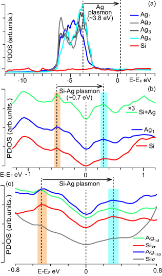
The atomic content of these peaks is mostly for the Si atoms and , for the Ag atom of the first slab layer [Fig. F1(b)], in agreement with recent DFT calculations 31 . Hence, the -like symmetry of the bands in the peeled phase is lost due to hybridization, which is likely to produce a hybridized plasmon.
Other PDOS peaks, expected to play a role in the EL function at absorbed energies ranging from to eV, do not correspond to any significant variation in the same EELS spectrum, which follows a smooth trend from the hybridized Si-Ag to the Ag plasmon resonances. We therefore expect that these PDOS structures, reported also in previous calculations 30 , are more and more smoothed by increasing the number of Ag layers, i.e., the number of bands, in the slab system.
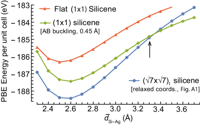
A more accurate insight into the role of hybridization comes from the analysis of the formation energy of the relaxed phase, as function of the distance between the silicene overlayer and the silver slab. In Fig. F3, we compare the total (PBE) energy per units cell required to have silicene and silicene (either in flat or buckled form) at an average distance from the topmost silver layer. We see that silicene is energetically favored for Å, whereas de-hybridized, buckled silicene is more likely to be formed for Å.
Thus, the reduced hybridization observed in the mixed phase, and the appearance of a plasmon structure compatible with silicene, is consistent with an average separation larger than Å of the three silicene domains relative the topmost silver layer. Interestingly enough, a similar value characterizes the binding of graphene on Cu(111), being a major factor for the survival of the Dirac-cone structure of the interface.
S2 Loss function of silicene and EELS spectrum of the phase
To distinguish the delicate features of the - plasmon in silicene, we discuss the energy-momentum features of the loss functions of the system in the energy range between and eV, where one-electron processes between occupied/empty bands of dominant and character are exclusively involved [see Fig. 6(b) and related discussion].
In Fig F4 we display the anisotropic dispersions of this mode along the and paths of the reciprocal space [Fig. 1(e) and inset in Fig. 4(b)]. When the Ag substrate, and its interaction with the silicene layer, is included in the calculations, the - mode is expected to survive, though being strongly contaminated by the aforementioned Si-Ag hybridization.
In support of this idea, the EELS data, labelled (ii) in Fig. 3, are juxtaposed in Fig. F5 to the theoretical EL curve of the superstructure. As noticed in the main text, the experimental low-energy peak at eV falls within the same energy-window of vertical transitions from the second VB to the first CB of silicene [Fig. 4(b)]. When Ag is included in the calculations, the electronic properties of the silicene layer change dramatically with respect to the peeled case, destroying the loss features at absorbed energies above eV.
On the other hand, a comparison of the DOS of the superstructure alone [Fig. 4(b)] with the different PDOS curves of the phase (Fig. F5) indicates that the low energy features associated to the band levels, at energies below eV from , are distorted but not completely erased. Indeed, the shapes and relative weights of the PDOS of the overlayer and the first Ag layer at these energies are similar, whereas other Ag layers produce a constant background.
This let us evince that the hybridization keeps traces of the peeled phase. More accurate studies are, though, needed to put a final word on this interpretation.
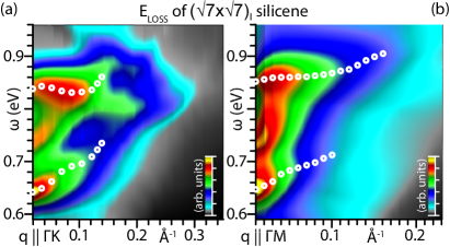
S3 -like plasmon mode of silicene vs EELS spectra of the mixed phase
The 2D plasmon nature of the -like plasmon of silicene has been scrutinized in a previous study 33 , where the effect of the - hybridization has been carefully addressed. Indeed, as shown in Fig. F6, the low-energy and low-momentum properties of the loss functions of the system describe a perfect two-dimensional mode with square-root-like dispersion along both and .
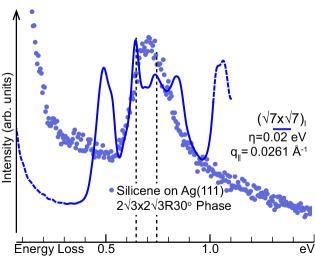
On the experimental side, Fig F7 shows EELS measurements on the mixed phase performed with the same geometry used for all the spectra of Fig. 3 at different scattering angles, obtained by rotating the analyzer in the range of to from the perpendicular direction to the sample.
What is apparently strange here, is that the frequency of the -like mode is subject to small variations, of the order of , vs significant changes in the scattering angle. These would correspond to in-plane momentum variations in the range of to Å-1, as predicted by the conservation of kinetic energy and in-plane momentum
typically used in EELS experiments, with =1.75-1.83 eV being the lower loss peak resonance.
The quasi dispersionless behavior observed here is carefully related to the morphological status of the silicene overlayer, i.e., to the mixed domains with juxtaposed diffraction patterns.
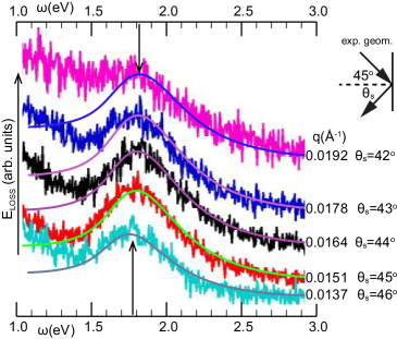
As recently demonstrated poli , truly dispersing plasmonic modes are achieved only in surfaces exhibiting large-scale, flat terraces. On the other hand, surfaces with extensive large-scale faceting and shattering are characterized by a nearly constant behavior of the plasmon dispersion, across the whole . In our case, the epitaxial growth of multiphase silicene inherently poses limits on the crystalline quality of the overlayer, which, owing to the different morphologies of the coexisting silicene superstructures, cannot possibly exhibit large-scale, flat terraces as single crystals of layered materials exfoliated with precision methods. This is confirmed upon comparing the LEED spots of Fig. 2(b) and the mixed reciprocal space of the ++ phase of Fig. 2(c), as suggested in the main text.
In typical EELS setups, the impinging electrons from the primary beam are reflected inside an extended electron-density distribution at the surface naza . In the presence of surface corrugation, these electrons are also reflected by the crests of the rough surface. Hence, the specular reflection of impinging electrons is inevitably lost due surface roughness. The experimental fingerprint of this phenomenon is the missing dependence of the intensity of reflected electrons on the scattering angle, which we have experienced in our EELS experiments. After scattering from the sample, the electrons are diffused by the crests of the rough surface in a wide solid angle. The corresponding excitation spectrum experimentally probed by EELS has then momentum-integrated spectral contributions with a maximum intensity due to low momenta. Thus the spectra of Fig. F7 are not resolved in in-plane momentum, but they are rather dominated by low-momentum excitations.
We may tentatively attribute a leading parallel momentum to the spectra, based on the theoretical loss curves computed from silicene with the TDDFT+RPA approach of the present work. As also shown in Fig. F7 the agreement is significant in all considered cases, which let us think that indeed the plasmon structure that we are observing is due to a quasi freestanding silicene overlayer.