Probing collective oscillation of –orbital electrons at the nanoscale
Abstract
Here we demonstrate that high energy electrons can be used to explore the collective oscillation of , , and orbital electrons at the nanometer length scale. Using epitaxial AlGaN/AlN quantum wells as a test system, we observe the emergence of additional features in the loss spectrum with increasing Ga content. A comparison of the observed spectra with ab–initio theory reveals the origin of these spectral features is attributed to 3–electrons contributed by Ga. We find that these modes differ in energy from the valence electron plasmons in Al1-xGaxN due to the different polarizability of the electrons. Finally, we study the dependence of observed plasmon modes on Ga content, lending insight into plasmon coupling with electron–-hole excitations.
The collective oscillation of free electrons (plasmons) is well described by the Drude model, which is based on the classical equations of motion for a free electron gas Jackson and Fox (1999); Pines (1966). In response to an externally applied electromagnetic field, the polarization of the electron gas generates a restoring force, creating longitudinal oscillatory modes in the Fermi sea. These modes can be sustained in any material at a characteristic frequency where the real part of the dielectric function goes to zero Ziman (1972), known as the plasma frequency, . For a free electron gas, , where is the density of electrons, and are the charge and mass of an electron, and is the permittivity. In spectroscopic studies of simple metals, this energy is also referred to as the “ultraviolet transmission limit”, since metals reflect photons with energy less than and transmit above this energy. This energy is very sensitive to the density of electrons in the Fermi sea undergoing oscillation, spanning a spectral range from the deep UV to far infrared. In particular, as the density of electrons varies from 1022 cm-3 (in simple metals) to 1010 cm-3 in (in dielectrics), this plasma energy varies from 4 eV to 4eV. In a typical semiconducting material such as silicon, the valence band is filled at room temperatures, with each atom contributing four electrons to the Fermi sea. This gives rise to a plasmon of energy 17eV. Since the electron density in the conduction band of a semiconductor is low at room temperature, collective oscillations of those electrons lie in the infra–red, and can only be probed by sensitive IR spectroscopy. Despite spanning this large spectroscopic range, the fundamental physics of these excitations is described with considerable success using the simple free electron model.
Within the free electron model, several important assumptions are made: all electrons in the system are treated as identical (or, equally “free”) , and the interactions between these electrons, as well as the influence of the periodic crystal potential generated by the “ion cores” in the solid are ignored Ziman (1972). Consequently, any interaction between “collective modes” i.e. plasmons, and the spectrum of single electron states (interband transitions) are not considered in the Drude model. In most metals, ignoring the periodic crystal potential is justified, since typical plasma frequencies (5-50 eV) are significantly higher than the energy of the single particle states (electron–hole pairs), and there is minimal admixing of plasmons and electrons. In wide band gap semiconductors, such as GaN ( = 3.4 eV) or AlN ( = 6 eV), however, solid–state effects are pronounced.
While plasmons in metals present a well defined, long lived excitation, the situation is considerably more complex in semiconductors where the influence of the crystal potential can not be ignored. The resultant plasmon coupling with the single particle electron–hole pair excitations (Landau damping), is an important decay channel through which plasmons dissipate energy, thus reducing plasmon lifetime. Several applications of plasmons have been proposed, such as the creation of a perfect lens Pendry (2000), invisibility cloaking Alù and Engheta (2005) or as conduits of on–chip signals which can interface naturally with optics Ozbay (2006). The realization of these exciting applications, however, requires knowledge of the various scattering mechanisms that affect plasmons and their relative importance. By mapping such plasmon modes at the nanometer scale, the role of interfaces, surfaces, and compositional fluctuations can be connected to plasmon scattering mechanisms in inhomogeneous media.
Features associated with plasmon creation are observed in spectroscopic techniques such as X-Ray absorption spectroscopy (XAS) and electron energy loss spectroscopy (EELS). While XAS typically offers better spectral resolution, EELS is capable of providing information at the atomic scale by scanning a finely-focused high energy electron probe across the sample Muller et al. (1999). For plasmon imaging, the spatial resolution is limited to nanometer length scales by delocalization of the plasmon excitation Egerton (1986). In the case of metal nanoparticles, this technique allows experimentalists to probe the dependence of the plasmon energy on particle shape Nelayah et al. (2007); Kociak et al. (2000), the coupling and energy splitting of plasmonic modes of particles separated by a nanoscale gap Koh et al. (2009); Agrawal et al. (2017), the mapping of surface plasmons Bosman et al. (2007), and the quantization of the plasmon modes Scholl et al. (2012). A collection of such results are presented in the review by Colliex et al. Colliex et al. (2016).
In this Letter, we analyze the plasmon loss signal in AlN/Al1-xGaxN quantum wells using scanning transmission electron microscopy (STEM) and EELS. We show that in addition to the primary plasmon peak (due to collective motion of the valence band electrons), two additional spectral features appear when Ga is present. We study the energies of these modes as a function of Ga composition and find that while the primary valence electron mode downshifts in energy, the additional modes shift to higher energies with increasing Ga fraction. Comparison with ab–initio calculations shows that these additional spectral features arise from the collective oscillation of Ga orbital electrons. Through this insight, we explain the dependence of plasmon energy on Ga composition, as well as changes in the peak linewidths, which sheds light on the relative importance of different plasmon scattering mechanisms.
AlN/Al1-xGaxN quantum well structures were grown by metal–organic chemical vapor deposition (MOCVD) on vicinal c-plane AlN and sapphire substrates as described previously Dalmau et al. (2011); Bryan et al. (2016). The quantum well width was varied between 2 nm and 50 nm and the composition range was varied between AlN (x = 0) and GaN (x = 1). Electron microscopy cross-sectional samples were wedge polished to electron transparency using an Allied Multiprep system Voyles et al. (2003). For final thinning, the samples were argon ion milled (Fischione Model 1050) at energies decreasing from 2 keV to 200 eV. A probe–corrected FEI Titan 60–300 kV STEM/TEM equipped with an X–FEG source was used for imaging and spectroscopy. Energy dispersive X-Ray spectroscopy was used to determine the composition of each quantum well, and was found to be in agreement with the expected values from the MOCVD conditions. The electron beam acceleration voltage was 80 keV to increase the cross–section of plasmon creation. Electron energy loss spectroscopy (EELS) was performed with a Gatan Enfinium ER spectrometer and with an energy spread of approximately 0.9 eV. As measured with the EELS log-ratio method, the sample thickness varied between 40 and 80 nm Malis et al. (1988). For plasmon energy and linewidth analysis, the spectra were first aligned relative to the zero–loss signal. The effects of plural scattering were then removed using Fourier-log deconvolution Egerton (1986). The plasmon loss peak was fit to the Drude model, where the permittivity of an electron gas with density is given by:
| (1) |
and the loss function is given by Im, which corresponds to a Lorentzian peak centered around the plasmon energy, , having a linewidth given by , where is the plasmon lifetime.

The EEL spectra shown in Figure 1(a) are acquired from quantum well structures with various Al1-xGaxN compositions. The different quantum wells, as in Figure 1(b), are otherwise similar in terms of sample thickness. The image intensity variation in Figure 1(b) results from the atomic number sensitivity of HAADF STEM and scales with Ga content. The variation of the valence plasmon energy across this quantum well structure is shown in Figure 1(c). Two trends are established from this data. First, increasing Ga incorporation leads to a downshift of the “primary” plasmon peak (p1) to lower energy. Second, additional energy loss signatures emerge at 24 (p2) and 28 (p3) eV. The downshift in the energy of the primary plasmon is a consequence of the decreasing band gap and the increasing unit cell volume with Ga content. Since both Al and Ga are group III elements, they both contribute 3 valence electrons per atom to the crystal. Hence, this increase in unit cell size leads to a decrease in valence electron density and consequently, a downshift in the plasma frequency (given by ). By mapping the position, width, and amplitude of these plasmon modes across the quantum well structures, one can spatially map the Ga fraction of these Al1-xGaxN alloys. This offers a complementary technique to methods such as EDS or quantitative STEM imaging for identifying the alloy composition Eljarrat et al. (2013); Amari et al. (2011) .
The emergence of two additional excitations at 24 eV and 28 eV can be understood by considering the difference in orbital configurations of Ga and Al. Ga contributes electrons to the Fermi sea due to its occupied 3– shell, while Al does not. To explore this, we examine results from ab–initio calculations of the Al1-xGaxN dielectric response in the random phase approximation. Many body effects are taken into account using the GW approximation. Rather than Drude’s classical description of a “free–electron” gas, we apply the Lindhard dielectric response theory Ziman (1972) to provide a rigorous framework for exploring plasmons in semiconducting materials. The Lindhard model describes a many–electron system in the influence of an external perturbation. This perturbation modifies the electron wavefunctions in this system, leading to a redistribution of charges, and hence the creation of an electrostatic potential. By ensuring self consistency between this generated response field and the original perturbation, we arrive at the following expression for permittivity:
| (2) |
where represents the probability of occupation of an electronic state with momentum and energy while is the frequency of the original perturbation, is the scattering wavevector, and is introduced to avoid singularities in the summation. It should be noted that this summation extends over all electronic states (occupied as well as unoccupied), denoted by their momentum quantum number . At energies much higher than the Fermi energy, states do not contribute to the summation as the numerator goes to zero. Using the random phase approximation, we calculate the permittivity of GaN, systematically increasing the number of electronic bands included in the summation sup .
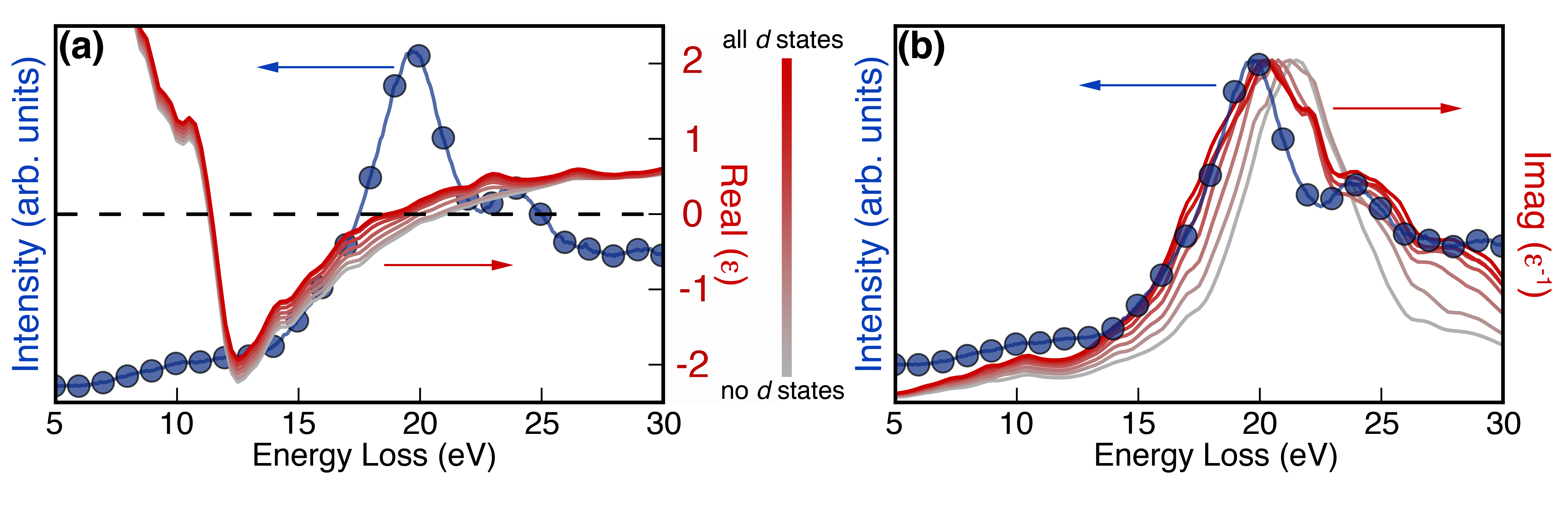
The results of the Lindhard model are shown in Figures 2(a) and (b), where the calculated real part of the dielectric function and the loss function (i.e, are provided along with experimental data. As the electronic states of the Ga 3– shell are included in the calculation, we observe the emergence of additional loss signatures at approximately 24 eV and 28 eV, in excellent agreement with experiment. When these states are excluded from the calculation, the loss function of GaN very closely resembles that of AlN. This leads to the conclusion that these additional features arise from the polarization of orbital electrons contributed to the crystal as Ga in incorporated in the lattice. In fact, upon revisiting the assumptions within the Drude model, one can see this is to be expected. The model Fermi sea used in the Drude picture assumes electrons live in plane waves states, and all electrons exist in the same parabolic band with the same effective mass. When various electronic bands, with different effective masses contribute to the Fermi sea, the emergence of additional modes is to be expected. This is also true for the AlGaN system, where the dispersions and effective masses for states is very different from those of the and orbital states (Figure S1). Similar observations have been made in graphitic systems for instance, where the and electrons are known to support different plasmon modes Luo et al. (2013).

Several different Al1-xGaxN compositions are also used to study the evolution of the energy-loss features as a function of Ga content, as in Figure 3. Explained above, the main bulk plasmon plasmon (p1), originating from the s and p valence electrons, downshifts as Ga composition is increased. In contrast, both p2 and p3 plasmon modes associated with –electrons, upshift as Ga is added. This provides additional evidence that the origin of these modes is the oscillation of orbital electrons. As Ga atoms are incorporated into the crystal structure, the number of available orbital electrons contributing to these modes increases, thus upshifting the plasmon energies of p2 and p3. Since Ga and Al contain the same number of outer shell s and p electrons, adding Ga does not change the number of electrons contributing to p1, and hence, this peak downshifts with the increasing unit cell size and reduced band gap Wang (1996). Note that while the difference in trends of p1 and p2 is obvious, the fitting uncertainty is considerably larger for p3, especially at low Ga compositions. Hence, we have left the discussion of fits to p3 in the supplemental document (Figure S2).
We also note the trends for the linewidth of these plasmons. As Ga fraction increases, we observe a sharpening of the plasmon peaks p1 and p2. In principle, these linewidths yield information about the plasmon excitation lifetime Wang (1996). Due to the broad energy spread of the electron beam, however, these linewidths provide only a qualitative measure of the various scattering rates. The excitation lifetime is determined by various scattering mechanisms such as interaction with phonons, or decay into electron–hole pairs, as well as disorder scattering due to alloying. If disorder related scattering due to compositional fluctuation were the dominant scattering mechanism, one expects the highest scattering rates at compositions around Al0.5Ga0.5N. This is not supported by trends presented in Figure 3. The results are, however, consistent with what can be expected if electron–plasmon coupling is dominant. Typically, the scattering rate between two quantum states is of the form , where is the coupling matrix element between states A and B, and and are the energies of these states. Hence, this scattering rate is inversely proportional to the difference in energies of the states being coupled. In the case here, is the energy of the valence electron plasmon (p1), and is the energy of an electron–hole pair. Since the band gap of GaN is much smaller than AlN, it is expected that the higher energy single electron states in AlN are more strongly coupled to plasmons than those in the lower band gap GaN. The plasmon linewidth is thus expected to broaden more for AlN than GaN, in agreement with our observation. Recent theoretical studies have predicted similar phenomena in semiconducting systems including emergence of new collective excitations and broadening due to electron–plasmon coupling in semiconductors Lischner et al. (2015); Vigil-Fowler et al. (2016); Caruso et al. (2015). A siimilar trend is observed in the linewidth evolution of the plasmon p2, however, the uncertainty from curve fitting is substantial for plasmons p3 due to poor signal-to-noise when Ga content is low. This uncertainty is also likely the cause of the anomalous linewidth evolution of the plasmon centered at 28 eV (shown in Figure S2). However, one can not rule out that this plasmon may be coupled differently to the single particle excitations owing to symmetry arguments of the electron–plasmon matrix element Dresselhaus et al. (2007).
The Nitride materials used in this study offer the ideal platform to observe such effects. The cyrstal growth of these materials is now mature to the point that solid–state phenomena are not washed out by defect scattering. Through the combination of experiment and theory, we have revealed the compositional dependence of 3–orbital plasmons using high energy electrons. By quantifying changes in the plasmon energies and linewidths, the influence of solid–state effects, such as electron–plasmon coupling is revealed in these wide band gap semiconductors. These results further demonstrate the applicability of low-loss EELS to probe subtle solid–state effects. Coupled with simultaneous atomic resolution STEM imaging, the approach can lead to spatial mapping of electron scattering pathways.
Acknowledgements.
The authors gratefully acknowledge support for this research from the Air Force Office of Scientific Research (FA9550-14-1-0182). JHD acknowledges support by the National Science Foundation Graduate Research Fellowship (DGE-1252376). This work was performed in part at the Analytical Instrumentation Facility (AIF) at North Carolina State University, which is supported by the State of North Carolina and the National Science Foundation (ECCS-1542015). The AIF is a member of the North Carolina Research Triangle Nanotechnology Network (RTNN), a site in the National Nanotechnology Coordinated Infrastructure (NNCI).References
- Jackson and Fox (1999) J. D. Jackson and R. F. Fox, American Journal of Physics 67, 841 (1999).
- Pines (1966) D. Pines, Elementary excitations in solids (Perseus, 1966).
- Ziman (1972) J. M. Ziman, Principles of the Theory of Solids (Cambridge university press, 1972).
- Pendry (2000) J. B. Pendry, Phys. Rev. Lett. 85, 3966 (2000).
- Alù and Engheta (2005) A. Alù and N. Engheta, Physical Review E 72, 016623 (2005).
- Ozbay (2006) E. Ozbay, science 311, 189 (2006).
- Muller et al. (1999) D. A. Muller, T. Sorsch, S. Moccio, F. Baumann, K. Evans-Lutterodt, and G. Timp, Nature 399, 758 (1999).
- Egerton (1986) R. Egerton, Springer, New York) p 226 (1986).
- Nelayah et al. (2007) J. Nelayah, M. Kociak, O. Stéphan, F. J. G. de Abajo, M. Tencé, L. Henrard, D. Taverna, I. Pastoriza-Santos, L. M. Liz-Marzán, and C. Colliex, Nature Physics 3, 348 (2007).
- Kociak et al. (2000) M. Kociak, L. Henrard, O. Stéphan, K. Suenaga, and C. Colliex, Physical Review B 61, 13936 (2000).
- Koh et al. (2009) A. L. Koh, K. Bao, I. Khan, W. E. Smith, G. Kothleitner, P. Nordlander, S. A. Maier, and D. W. McComb, Acs Nano 3, 3015 (2009).
- Agrawal et al. (2017) A. Agrawal, A. Singh, S. Yazdi, A. Singh, G. K. Ong, K. Bustillo, R. W. Johns, E. Ringe, and D. J. Milliron, Nano Letters (2017).
- Bosman et al. (2007) M. Bosman, V. J. Keast, M. Watanabe, A. I. Maaroof, and M. B. Cortie, Nanotechnology 18, 165505 (2007).
- Scholl et al. (2012) J. A. Scholl, A. L. Koh, and J. A. Dionne, Nature 483, 421 (2012).
- Colliex et al. (2016) C. Colliex, M. Kociak, and O. Stéphan, Ultramicroscopy 162, A1 (2016).
- Dalmau et al. (2011) R. Dalmau, B. Moody, R. Schlesser, S. Mita, J. Xie, M. Feneberg, B. Neuschl, K. Thonke, R. Collazo, A. Rice, J. Tweedie, and Z. Sitar, Journal of The Electrochemical Society 158, H530 (2011).
- Bryan et al. (2016) I. Bryan, Z. Bryan, S. Mita, A. Rice, L. Hussey, C. Shelton, J. Tweedie, J.-P. Maria, R. Collazo, and Z. Sitar, Journal of Crystal Growth 451, 65 (2016).
- Voyles et al. (2003) P. Voyles, J. Grazul, and D. Muller, Ultramicroscopy 96, 251 (2003).
- Malis et al. (1988) T. Malis, S. Cheng, and R. Egerton, Journal of electron microscopy technique 8, 193 (1988).
- Eljarrat et al. (2013) A. Eljarrat, L. López-Conesa, C. Magén, Ž. Gačević, S. Fernández-Garrido, E. Calleja, S. Estradé, and F. Peiró, Microscopy and Microanalysis 19, 698 (2013).
- Amari et al. (2011) H. Amari, H. Zhang, L. Geelhaar, C. Chèze, M. Kappers, and T. Walther, in Journal of Physics: Conference Series, Vol. 326 (IOP Publishing, 2011) p. 012039.
- (22) “See supplemental material at [url] for additional details on calculation of dielectric response.” .
- Luo et al. (2013) X. Luo, T. Qiu, W. Lu, and Z. Ni, Materials Science and Engineering: R: Reports 74, 351 (2013).
- Wang (1996) Z. Wang, Micron 27, 265 (1996).
- Lischner et al. (2015) J. Lischner, G. Pálsson, D. Vigil-Fowler, S. Nemsak, J. Avila, M. Asensio, C. Fadley, and S. G. Louie, Physical Review B 91, 205113 (2015).
- Vigil-Fowler et al. (2016) D. Vigil-Fowler, S. G. Louie, and J. Lischner, Physical Review B 93, 235446 (2016).
- Caruso et al. (2015) F. Caruso, H. Lambert, and F. Giustino, Physical review letters 114, 146404 (2015).
- Dresselhaus et al. (2007) M. S. Dresselhaus, G. Dresselhaus, and A. Jorio, Group theory: application to the physics of condensed matter (Springer Science & Business Media, 2007).