Impact of second-order piezoelectricity on electronic and optical properties of -plane InxGa1-xN quantum dots: Consequences for long wavelength emitters
Abstract
In this work we present a detailed analysis of the second-order piezoelectric effect in -plane InxGa1-xN/GaN quantum dots and its consequences for electronic and optical properties of these systems. Special attention is paid to the impact of increasing In content on the results. We find that in general the second-order piezoelectric effect leads to an increase of the electrostatic built-in field. Furthermore, our results show that for an In content 30% this increase in the built-in field has a significant effect on the emission wavelength and the radiative lifetimes. For instance, at 40% In, the radiative lifetime is more than doubled when taking second-order piezoelectricity into account. Overall our calculations reveal that when designing and describing the electronic and optical properties of -plane InxGa1-xN/GaN quantum dot based light emitters with high In contents, second-order piezoelectric effects cannot be neglected.
Heterostructures based on InxGa1-xN alloys are of great technological interest thanks to its bandgap energy tunability with changing In content . Nakamura et al. (1996); Matioli et al. (2011); Nakamura and Fasol (1997) By changing , in principle, wavelengths between ultraviolet ( eV) and the near infrared regime ( eV) are achievable. Thus, this ideally broad range spans the entire visible spectrum, rendering the material highly suitable for use in optoelectronic devices such as light-emitting diodes, laser diodes and solar cells. Nakamura et al. (1996); Matioli et al. (2011); Nakamura and Fasol (1997) Utilizing InxGa1-xN/GaN based quantum well (QW) structures, high efficiency devices operating in the violet and blue spectral region have been realized over the last few years. Nakamura (2015); Shen et al. (2015) However, keeping the efficiency high and extending the emission wavelength into the green, yellow or infrared wavelength range by increasing the In content is still challenging. Jiang et al. (2015); Du et al. (2014) Several factors contribute to this so-called “green gap” problem, Humphreys et al. (2017) ranging from sample quality, due to large strains in QW systems, up to strong strain-induced electrostatic piezoelectric fields. The piezoelectric effect leads, for instance, to a spatial separation of electron and hole wave functions and in turn to increased radiative lifetimes, also known as the quantum confined Stark effect (QCSE). pu Wan, bai Xia, and Chang (2001) However, theoretical studies have shown that the built-in field is strongly reduced in an InxGa1-xN/GaN quantum dot (QD) when compared to a QW of the same height and In content. Schulz and O’Reilly (2010) This originates from strain relaxation mechanism and surface area effects, stemming from the three dimensional QD confinement, and results in a reduction of the QCSE in QDs. Therefore, for an InxGa1-xN/GaN QD, when compared to a InxGa1-xN/GaN QW of the same height, the In content in the dot can be increased considerably for a comparable field in both systems. This suggests that InxGa1-xN/GaN QDs are promising candidates to achieve efficient radiative recombination at longer wavelength. Recently, making use of this concept, InxGa1-xN/GaN QD based light emitters operating in the green to yellow spectral range have been realized. Weng et al. (2016); Mei et al. (2017) Moreover, Frost and co-workers Frost et al. (2016); Su et al. (2015) have demonstrated high performance red emitting (630 nm) lasers using InxGa1-xN/GaN QDs. To achieve this emission wavelength, In contents as high as 40% have been reported. Frost et al. (2016) Only a few theoretical studies have addressed the electronic and optical properties of these high In content, long wavelength emitters. Su et al. (2015); Khoshnegar et al. (2010) Additionally, piezoelectric fields in thin InN layers, embedded in GaN, have been used to achieve topological insulator states. Miao et al. (2012) However, all previous theoretical studies on these different aspects of InGaN/GaN based systems included linear piezoelectric polarization contributions only. Recently, non-linear piezoelectricity effects have been discussed and reported for wurtzite III-N QW systems. Pal et al. (2011); Prodhomme, Beya-Wakata, and Bester (2013); Migliorato et al. (2014) These studies showed for instance better agreement between theoretical and experimental built-in field values when second-order piezoelectric effects are considered in the calculations. Furthermore, in other material systems, such as zincblende InAs/GaAs QDs, second-order piezoelectric effects have been highlighted to affect their electronic and optical properties significantly. Bester et al. (2006a, b); Schliwa, Winkelnkemper, and Bimberg (2007) However, no detailed study exists on the importance of second-order piezoelectricity on electronic and optical properties of -plane InxGa1-xN dots with varying In content. Given the recent drive for InxGa1-xN QD based light emitters with high In contents (), the question of how important second-order piezoelectric effects are for describing and designing these emitters for future optoelectronic devices is of central importance.
Here, we address this question by calculating electronic and optical properties of -plane InxGa1-xN/GaN QDs with In contents ranging from 10% to 50% using a continuum based model, including the full second-order piezoelectric polarization vector. We find that the second-order piezoelectric effect leads to an increase in the electrostatic built-in field when compared to the situation where only standard first-order contributions are accounted for. This increase in the built-in field, at least for the structures studied here, is of secondary importance for emission wavelength and radiative lifetime of -plane dots with In contents in the range of 10% to 20%. However, for In contents of order 40%, our calculations show that second-order piezoelectricity has a significant effect on these quantities. For instance, at , we observe that for the chosen QD geometry the radiative lifetime is more than doubled when comparing a calculation that includes second-order piezoelectric effects to one neglecting this contribution. Consequently, second-order piezoelectricity has to be taken into account when designing nanostructures operating in the long wavelength, high In content regime.
The total strain induced piezoelectric polarization () in a semiconductor material with a lack of inversion symmetry can be written, up to second-order, as Bester et al. (2006a)
| (1) |
Here is the first order contribution and is the second-order part. The first-order piezoelectric coefficients are denoted by and are second-order ones. The strain tensor components (in Voigt notation) are given by . From Eq. (1) one can infer already that second-order piezoelectricity should become important for systems under large strains, in our case high In contents, given that it is related to products of strain tensor components.
For wurtzite semiconductors the well known first-order contribution has only three independent piezoelectric coefficients, namely , and . Andreev and O’Reilly (2000) For the second-order coefficients , Grimmer Grimmer (2007) showed that out of 36 coefficients, 17 are nonzero of which 8 are independent. Taking all this into account and using cartesian notation for the strain tensor, in a wurtzite -plane system the total (first plus second-order) piezoelectric polarization vector field is given by
| (2) | |||||
It should be noted that this expression is far more complicated when compared to piezoelectric effects in zincblende structures. In the zincblende case one is left with only one first-order and three independent second-order piezoelectric coefficients. Bester et al. (2006a); Grimmer (2007)
| (a) First-order + spontaneous | (b) Second-order | (c) Total |
|---|---|---|
 |
 |
 |
To analyze the impact of second-order piezoelectricity on the electronic and optical properties of -plane InxGa1-xN/GaN QDs with varying In content , we have performed continuum-based calculations by means of theory. All calculations have been carried out in the highly flexible plane wave based software library S/PHI/nX, Marquardt et al. (2014) allowing us to define customized piezoelectric polarization vector fields such as Eq. (2). In doing so, we are able to perform calculations in the presence and absence of second-order piezoelectricity. Additionally, spontaneous polarization effects are included in the calculations, with values for GaN and InN taken from Ref. Caro, Schulz, and O’Reilly, 2013, and the bowing parameter from Ref. Vurgaftman and Meyer, 2003. First-order piezoelectric coefficients from Ref. Caro, Schulz, and O’Reilly, 2013 and second-order coefficients from Ref. Prodhomme, Beya-Wakata, and Bester, 2013 have been used. For the electronic structure calculations we have applied a six-band Hamiltonian to describe the hole states and a single-band effective mass approximation for electron states. This model accounts for valence band mixing effects and the differences in the effective masses along different directions. Since we are mainly interested in e.g. wavelength shifts due to second-order piezoelectricity, the applied electronic structure approach is sufficient for our purposes. Further refinements can be achieved by applying an eight-band model. Miao et al. (2012) Using the wave functions, the radiative lifetime of the electron and hole ground state transition has been calculated, Patra et al. (2017); Fonoberov and Balandin (2003) employing a light polarization vector perpendicular to the sample surface. More details on theoretical framework and parameter sets applied are given in Refs. Patra and Schulz, 2017; Marquardt et al., 2014; Patra, Marquardt, and Schulz, 2016; Patra et al., 2017.
Following previous studies on InxGa1-xN QDs, we have assumed a lens-shaped dot geometry. Barthel et al. (2013); Schulz and O’Reilly (2010) Based on earlier atomic force microscopy results, a QD base diameter of nm and a dot height of nm has been chosen. Moriwaki et al. (2000); Sénès et al. (2007) Here our main focus is on how electronic and optical properties of -plane InxGa1-xN QDs change with increasing In content when second-order piezoelectric effects are considered. Thus, we vary the In content of the dot between 10% and 50% in 10% steps.
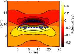
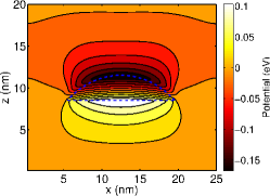
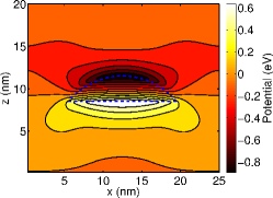
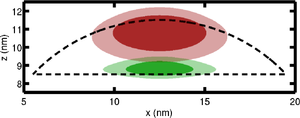
In a first step we analyze how the built-in potential in a -plane InxGa1-xN/GaN QD is changed when including second-order piezoelectric effects. Contour plots of the built-in potential of a -plane In0.5Ga0.5N dot, for a slice through the QD center, are shown in Fig. 1. The slice is taken in the -plane, where the -axis is parallel to the wurtzite -axis. The impact of changes in the In content will be investigated below when we discuss electronic and optical properties of the structures under consideration. In Fig. 1 (a) the built-in potential arising from the standard first-order piezoelectric contribution and the spontaneous polarization is shown. The well known potential drop along the -axis, leading to a spatial separation of electron and hole wave functions, is clearly visible. Figure 1 (b) depicts the second-order piezoelectric contribution only. Here, several features are of interest. First, the magnitude of the second-order contribution, even at , is a factor of order 4 smaller compared to the situation where only first-order piezoelectricity and spontaneous polarization are taken into account (cf. Fig. 1 (a)). Nevertheless, the second-order contribution has still a sizeable magnitude. Second, the symmetry of the second-order contribution and the potential profile are similar to the first-order contribution (cf. Fig. 1 (a)). Thus, when taking second-order piezoelectric effects into account, the potential drop across the QD will be larger, leading to an even stronger electrostatic built-in field and thus to an even stronger spatial separation of electron and hole wave functions. We will come back to this effect below. The fact that the second-order built-in potential contribution is of the same symmetry as the first-order term is for instance different to zincblende InAs/GaAs QDs. Bester et al. (2006a) Additionally, it should be noted that the magnitude of the second-order piezoelectric contribution also depends on the QD shape and size, as highlighted by Schliwa et al. Schliwa, Winkelnkemper, and Bimberg (2007) for InGaAs/GaAs QD systems. To gain initial insights into this question for InGaN QDs, we have performed additional calculations for a slightly larger dot ( nm, nm) with 30% In. This study reveals only a slight increase in the potential drop across the nanostructure when compared to a In0.3Ga0.7N dot with nm and nm. For different QD geometries and/or higher dots this situation might change. However, a detailed analysis of the impact of QD shape and size is beyond the scope of the present study. Here, we are interested in establishing trends with increasing In content. Figure 1 (c) shows the total (spontaneous+first-order+second-order) built-in potential for the considered lens-shaped -plane In0.5Ga0.5N QD. As expected from the discussion above, when including second-order piezoelectric effects, the total potential drop is clearly increased compared to the situation where only first-order piezoelectricity and spontaneous polarization are considered (cf. Fig. 1 (a)). The question is now, how strongly are electronic and optical properties affected when taking second-order piezoelectric effects into account? In the following we will look at the impact of second-order piezoelectricity on the emission wavelength and the radiative lifetime as a function of the dot In content . But before turning to these questions, we start with looking at the electron and hole ground state charge densities of the In0.5Ga0.5N QD. Figure 2 shows the isosurfaces of the electron (red) and hole (green) ground state charge densities. In Fig. 2 (a) results in the absence of the second-order piezoelectric effect are shown; (b) depicts the data originating from a calculation accounting for the full built-in potential, thus including second-order piezoelectricity. From Fig. 2 we can conclude that the increase in the built-in potential due to second-order piezoelectricity leads to a stronger spatial separation of the carriers along the -axis. Thus the wave function overlap is reduced and consequently the radiative lifetime will increase. Also, due to the increased built-in potential, an increased red shift of the emission wavelength due to second-order piezoelectricity is expected.
| First-order + spontaneous |
 |
| Total |
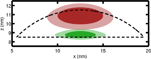 |
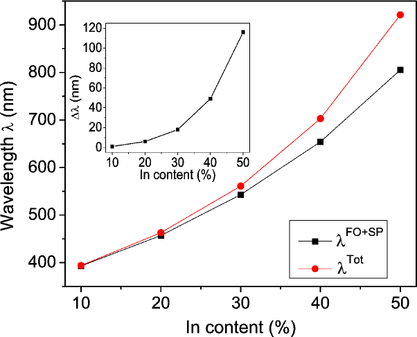
Figure 3 shows the emission wavelength of the here considered -plane InxGa1-xN/GaN QD for In contents varying between 10% and 50%. The black squares () denote the results in the absence of second-order contributions [only first-order (FO) piezoelectricity and spontaneous (SP) polarization], while the red circles () show the data when including also second-order piezoelectric effects. Again, it should be noted that for emitters operating in the red wavelength regime, In contents of 40% have been reported in the literature, Frost et al. (2016) so that the here studied In content range is relevant to recent experimental studies. From Fig. 3 one can infer that for lower In contents (up to 20%), the second-order piezoelectric contribution has little effect on . In fact in this case the difference in the emission wavelength , obtained from a calculation with spontaneous and first-order piezoelectric polarization only, , and a calculation including second-order piezoelectric effects, , is less than 10 nm. To show this effect more clearly, the inset in Fig. 3 depicts as a function of the In content . Between 30% and 40% In, second-order effects lead to a noticeable difference, resulting in values of approximately 20 nm to 50 nm, respectively. At 50% In we observe a wavelength shift of nm. Overall, the wavelength shift is almost equally distributed between electron and hole ground state energy shifts. We attribute this to the combined effect of differences in electron and hole effective masses and the asymmetry in the magnitude of the built-in potential between the upper and lower QD interface. Moreover, the change in the confinement potential due to second-order piezoelectricity might also affect the Coulomb interaction between the carriers and can lead to further contributions to the wavelength shift discussed here in the single-particle picture. Overall, our calculations reveal two things. First, when targeting QD-based emitters operating in the red spectral regime ( 650 nm), second-order piezoelectric effects can play a significant role. Furthermore, the second-order piezoelectric contribution shifts the emission to longer wavelength. Thus, when designing emitters operating in this long wavelength regime, the required In content predicted from a model including second-order effects would be lower as expected from a “standard model”, which accounts for first-order piezoelectric effects and spontaneous polarization only.
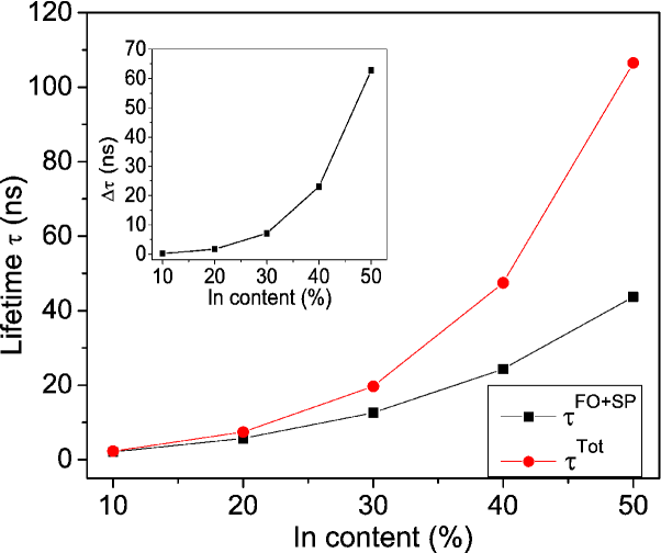
Even though our analysis indicates that lower In contents are sufficient to reach emission at longer wavelength, the increase in the built-in potential responsible for this effect will have a detrimental effect on the wave function overlap and consequently on the radiative lifetime . To study the impact of second-order piezoelectricity on the radiative lifetime , Fig. 4 depicts in the absence (, black squares) and in the presence (, red circles) of second-order piezoelectric contributions. Similar to the wavelength shift discussed above, in the In content range of 10% to 20% the influence of second-order piezoelectricity is of secondary importance ( ns). The inset of Fig. 4 depicts the difference in the radiative lifetime , obtained from calculations including () and neglecting () second-order piezoelectric contributions. The calculated radiative lifetimes in the 10% to 20% In regime are in the range of 3 ns to 10 ns, which is in good agreement with reported experimental data on these systems Robinson et al. (2003); Jarjour et al. (2007). However, for higher In contents we clearly observe a significant contribution from second-order piezoelectricity. At 30% the value is a factor of order 1.5 larger ( ns; ns) when including second-order piezoelectric effects in the calculations. At 40% and 50% In, the value of becomes 23 ns and 62 ns, respectively. But, it should be noted that the here calculated radiative lifetimes for a -plane In0.4Ga0.6N QD, even without second-order effects, are much larger than the experimental values ( ns) reported in the literature for InGaN dots with 40% In. Frost et al. (2016) Further studies, both theoretically and experimentally, are required to shed more light onto the physics of InxGa1-xN QDs operating in the long wavelengths regime (green to red).
In summary, we have presented a detailed analysis of the impact of second-order piezoelectricity on the electronic and optical properties of -plane InxGa1-xN/GaN QDs. Our study revealed that the second-order piezoelectric effect leads to an increase in the built-in field when compared to calculations taking only first-order piezoelectricity and spontaneous polarization into account. However, when looking at emission wavelength shifts or radiative lifetime values, at In contents around 10% to 20%, these quantities are almost unaffected by second-order piezoelectricity. But, when exceeding 30% In, both quantities are affected significantly by second-order contributions. The second-order piezoelectric effect induced built-in field increase leads to the situation that the emission is shifted to longer wavelength in comparison to a calculation based on spontaneous and first-order piezoelectric polarization effects only. This means that when accounting for second-order effects, lower In contents can be considered to reach for instance emission in the red spectral region. On the other hand, the increase in the built-in potential due to second-order piezoelectric contributions results in a strong increase in the radiative lifetime for long wavelength, high In content emitters when compared to results from a “standard” first-order study. Overall, our results reveal that when targeting InxGa1-xN QD-based emitters operating in the yellow to red spectral regime, second-order piezoelectricity cannot be neglected and should be taken into account for designing and understanding the electronic and optical properties of these systems.
This work was supported by Science Foundation Ireland (project number 13/SIRG/2210). The authors would like to thank Brian Corbett, Eoin P. O’Reilly and Miguel A. Caro for fruitful discussions.
References
- Nakamura et al. (1996) S. Nakamura, M. Senoh, S. ichi Nagahama, N. Iwasa, T. Yamada, T. Matsushita, H. Kiyoku, and Y. Sugimoto, Jpn. J. Appl. Phys. 35, L74 (1996).
- Matioli et al. (2011) E. Matioli, C. Neufeld, M. Iza, S. C. Cruz, A. A. Al-Heji, X. Chen, R. M. Farrell, S. Keller, S. DenBaars, U. Mishra, S. Nakamura, J. Speck, and C. Weisbuch, Appl. Phys. Lett. 98, 021102 (2011).
- Nakamura and Fasol (1997) S. Nakamura and G. Fasol, The Blue Laser Diode (Springer, 1997).
- Nakamura (2015) S. Nakamura, Rev. Mod. Phys. 87, 1139 (2015).
- Shen et al. (2015) H. Shen, W. Cao, N. T. Shewmon, C. Yang, L. S. Li, and J. Xue, Nano Lett. 15, 1211 (2015).
- Jiang et al. (2015) Y. Jiang, Y. Li, Y. Li, Z. Deng, T. Lu, Z. Ma, P. Zuo, L. Dai, L. Wang, H. Jia, W. Wang, J. Zhou, W. Liu, and H. Chen, Sci. Rep. 5, 10883 (2015).
- Du et al. (2014) C. Du, Z. Ma, J. Zhou, T. Lu, Y. Jiang, P. Zuo, H. Jia, and H. Chen, Appl. Phys. Lett. 105, 071108 (2014).
- Humphreys et al. (2017) C. Humphreys, J. Griffiths, F. Tang, F. Oehler, S. Findlay, C. Zheng, J. Etheridge, T. Martin, P. Bagot, M. Moody, D. Sutherland, P. Dawson, S. Schulz, S. Zhang, W. Fu, T. Zhu, M. Kappers, and R. Oliver, Ultramicroscopy 176, 93 (2017).
- pu Wan, bai Xia, and Chang (2001) S. pu Wan, J. bai Xia, and K. Chang, J. Appl. Phys. 90, 6210 (2001).
- Schulz and O’Reilly (2010) S. Schulz and E. P. O’Reilly, Phys. Rev. B 82, 033411 (2010).
- Weng et al. (2016) G. Weng, Y. Mei, J. Liu, W. Hofmann, L. Ying, J. Zhang, Y. Bu, Z. Li, H. Yang, and B. Zhang, Opt. Express 24, 15546 (2016).
- Mei et al. (2017) Y. Mei, G.-E. Weng, B.-P. Zhang, J.-P. Liu, W. Hofmann, L.-Y. Ying, J.-Y. Zhang, Z.-C. Li, H. Yang, and H.-C. Kuo, Light Sci Appl. 6, e16199 (2017).
- Frost et al. (2016) T. Frost, A. Hazari, A. Aiello, M. Z. Baten, L. Yan, J. Mirecki-Millunchick, and P. Bhattacharya, Jpn. J. Appl. Phys. 55, 032101 (2016).
- Su et al. (2015) G.-L. Su, T. Frost, P. Bhattacharya, and J. M. Dallesasse, Opt. Express 23, 12850 (2015).
- Khoshnegar et al. (2010) M. Khoshnegar, M. Sodagar, A. Eftekharian, and S. Khorasani, IEEE J. Quant. Electron. 46, 228 (2010).
- Miao et al. (2012) M. S. Miao, Q. Yan, C. G. Van de Walle, W. K. Lou, L. L. Li, and K. Chang, Phys. Rev. Lett. 109, 186803 (2012).
- Pal et al. (2011) J. Pal, G. Tse, V. Haxha, M. A. Migliorato, and S. Tomić, Phys. Rev. B 84, 085211 (2011).
- Prodhomme, Beya-Wakata, and Bester (2013) P.-Y. Prodhomme, A. Beya-Wakata, and G. Bester, Phys. Rev. B 88, 121304 (2013).
- Migliorato et al. (2014) M. A. Migliorato, J. Pal, R. Garg, G. Tse, H. Y. Al-Zahrani, U. Monteverde, S. Tomić, C.-K. Li, Y.-R. Wu, B. G. Crutchley, I. P. Marko, and S. J. Sweeney, AIP Conference Proceedings 1590, 32 (2014).
- Bester et al. (2006a) G. Bester, A. Zunger, X. Wu, and D. Vanderbilt, Phys. Rev. B 74, 081305 (2006a).
- Bester et al. (2006b) G. Bester, X. Wu, D. Vanderbilt, and A. Zunger, Phys. Rev. Lett. 96, 187602 (2006b).
- Schliwa, Winkelnkemper, and Bimberg (2007) A. Schliwa, M. Winkelnkemper, and D. Bimberg, Phys. Rev. B 76, 205324 (2007).
- Andreev and O’Reilly (2000) A. D. Andreev and E. P. O’Reilly, Phys. Rev. B 62, 15851 (2000).
- Grimmer (2007) H. Grimmer, Acta Crystallogr. Sect. A 63, 441 (2007).
- Marquardt et al. (2014) O. Marquardt, S. Boeck, C. Freysoldt, T. Hickel, S. Schulz, J. Neugebauer, and E. P. O’Reilly, Computional Materials Science 95, 280 (2014).
- Caro, Schulz, and O’Reilly (2013) M. A. Caro, S. Schulz, and E. P. O’Reilly, Phys. Rev. B 88, 214103 (2013).
- Vurgaftman and Meyer (2003) I. Vurgaftman and J. R. Meyer, J. Appl. Phys. 94, 3675 (2003).
- Patra et al. (2017) S. K. Patra, T. Wang, T. J. Puchtler, T. Zhu, R. A. Oliver, R. A. Taylor, and S. Schulz, phys. status solidi (b) 254, 1600675 (2017).
- Fonoberov and Balandin (2003) V. A. Fonoberov and A. A. Balandin, J. Appl. Phys. 94, 7178 (2003).
- Patra and Schulz (2017) S. K. Patra and S. Schulz, J. Phys. D: Appl. Phys. 50, 025108 (2017).
- Patra, Marquardt, and Schulz (2016) S. K. Patra, O. Marquardt, and S. Schulz, Opt. Quant. Electron. 48, 151 (2016).
- Barthel et al. (2013) S. Barthel, K. Schuh, O. Marquardt, T. Hickel, J. Neugebauer, F. Jahnke, and G. Czycholl, Eur. Phys. J. B 86, 449 (2013).
- Moriwaki et al. (2000) O. Moriwaki, T. Someya, K. Tachibana, S. Ishida, and Y. Arakawa, Appl. Phys. Lett. 76, 2361 (2000).
- Sénès et al. (2007) M. Sénès, K. L. Smith, T. M. Smeeton, S. E. Hooper, and J. Heffernan, Phys. Rev. B 75, 045314 (2007).
- Robinson et al. (2003) J. W. Robinson, J. H. Rice, A. Jarjour, J. D. Smith, R. A. Taylor, R. A. Oliver, G. A. D. Briggs, M. J. Kappers, C. J. Humphreys, and Y. Arakawa, Appl. Phys. Lett. 83, 2674 (2003).
- Jarjour et al. (2007) A. F. Jarjour, R. A. Oliver, A. Tahraoui, M. J. Kappers, C. J. Humphreys, and R. A. Taylor, Phys. Rev. Lett. 99, 197403 (2007).