Journal of Applied Physics 122, 055301 (published online 2 August 2017)Quantum efficiency modeling for a thick back-illuminated astronomical CCD
Abstract
The quantum efficiency and reflectivity of thick, back-illuminated CCD’s being fabricated at LBNL for astronomical applications are modeled and compared with experiment. The treatment differs from standard thin-film optics in that (a) absorption is permitted in any film, (b) the 200–500 m thick silicon substrate is considered as a thin film in order to observe the fringing behavior at long wavelengths, and (c) by using approximate boundary conditions, absorption in the surface films is separated from absorption in the substrate. For the quantum efficiency measurements the CCD’s are normally operated as CCD’s, usually at C, and at higher temperatures as photodiodes. They are mounted on mechanical substrates. Reflectivity is measured on air-backed wafer samples at room temperature. The agreement between model expectation and quantum efficiency measurement is in general satisfactory.
pacs:
42.30LrI Introduction
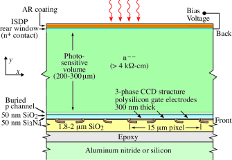
Fully depleted thick back-illuminated p-channel charge-coupled devices (CCD’s) developed at Lawrence Berkeley National Laboratory (LBNL) for astronomical applications have useful quantum efficiencies (QE’s) extending into the near infrared (IR)Holland et al. (2003, 2006). The response is limited to 1100 nm by the indirect bandgap of silicon. The QE typically falls to about 50% at 1000 nm, depending on the temperature and thickness of the CCD. Thicknesses range from 200 to 500 m. The temperature range of interest is C to 20∘ C. If C, the QE is measured by operating the device as a photodiode. A highly schematic cross section of a typical back-illuminated LBNL CCD is shown in Fig. 1.
Modeling the response depends crucially on the complex refractive indices and thicknesses of the materials involved. Especially critical is the absorption coefficient of silicon as the indirect bandgap is approached. Most of the other indices also present special problems.
While the formalism presented here is applicable to any CCD, we specialize to the LBNL case. In these CCD’s, a thin film (10–25 nm) of in-situ doped polysilicon (ISDP) is grown on the rear surface to serve as an ohmic contact. Absorption in this layer limits the blue response, particularly below 450 nm. Over the ISDP is an antireflective coating optimized for maximum transmission at desired wavelengths, particularly in the near-infrared.
This paper and the corresponding code grew out of work reported by GroomGroom et al. (1999) in 1999. At that time the treatment of absorption in the ISDP and surface films was ad hoc at best. Absorption by an indium-tin oxide (ITO) film was neglected. ISDP absorption was poorly modeled, so that results below about 550 nm were uncertain.
Although oblique incidence with either and parallel to the surface is treated, oblique incidence is of relatively little importance, since even for the extreme case of an f1 system the incident is , and the ray is “quickly straightened” by refraction into the high-index silicon (–4).
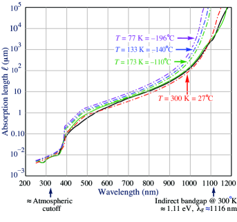
The design constraints are daunting: As shown in Fig. 2, the absorption length in silicon ranges over four orders of magnitude in the useful wavelength region, from a few nm at the atmospheric cutoff near 320 nm to the thickness of the CCD, typically 250 m. At the blue end of the spectrum it is close to the thickness of the (absorptive) ISDP, while at the near-IR end the CCD approaches transparency, with multiple reflections producing fringes.
The analysis uses the standard transfer matrix formalism described in multiple sources, e.g. in Refs. Pedrotti and Pedrotti, 1993; Hecht, 1998; Macleod, 2001. Some departures are made in addressing CCD-specific absorption issues:
-
1.
Many sources do not consider absorption—after all, one tries to make optical coatings out of transparent materials. But once it is introduced, there is a sign ambiguity in the definition of the complex index of refraction: or . The choice is arbitrary: The positive convention is used in Refs. Hecht, 1998; Macleod, 2001; Jenkins and White, 1950; Panofsky and Phillips, 1955; Slater and Frank, 1947, while the negative convention is used in Refs. Born and Wolf, 1999; Pedrotti and Pedrotti, 1993; Sommerfeld, 1964. Having chosen the sign, one must take care that the rest of the formalism ensures that light is attenuated in absorptive layers. We adopt the negative sign convention.
-
2.
The silicon substrate is also treated as a “thin film,” although it is opaque over much of the optical range of interest. Fringes are commonly observed near the red end of a back-illuminated CCD’s sensitivity, implying coherence over the thickness of the device and, remarkably, near-specular reflection from the front surface gate structure and mechanical substrate. For a 200 m thick CCD the fringe spacing at nm is only 0.7 nm, and in any case the fringes are “washed out” by a finite aperture.
-
3.
It is useful to find absorption in the antireflective (AR) coating and, separately, in the ISDP. This is done by modifying boundary conditions, valid when the absorption length in silicon is small compared to the substrate thickness.
We assume 100% internal quantum efficiency, i.e., every photon absorbed in the sensitive region produces a collected electron or hole.
Model and measurement results are discussed for three antireflective coating designs: ITO/SiO2, ITO/ZrO2/SiO2, and TiO2/SiO2.
II Multilayer reflected and transmitted amplitudes and intensities
In the simplest case, a plane wave in medium with real index (usually air or vacuum) is incident at an angle on a film with complex index and thickness . It exits into medium with index . With the definition (appropriate if is parallel to the surface), the boundary conditions relate the fields at the two interfaces:
| (1) |
The phase lag in one traversal, , is . The product can be calculated from the complex version of Snell’s law:
| (2) |
The transport matrix contains only variables pertaining to that layer; if the light is transmitted into another film a similar matrix is introduced. For films,
| (3) |
The reflected fraction of the light and the transmitted fraction can be extracted from the boundary condition equations,
| (4a) | |||||
| (4b) | |||||
where the are the components of the product matrix .
Over most of the spectral region of interest, the silicon substrate is essentially opaque. More specifically, and both contain potentially large factors . While it is easy to block numerical overflows, we have found it convenient to factor out the divergent behavior:
| (5) |
Here is the imaginary part of , and, because of our negative sign convention for the imaginary part of indices, it is always negative. Eqs. (4) become
| (6a) | |||||
| (6b) | |||||
Since the exponential factors cancel in Eq. (6a), the reflected amplitude is calculable for any amount of absorption, while the transmitted amplitude is (essentially) zero for high absorption.
If is parallel to the surface, then . Since the phase lag is geometrical, it is not affected by polarization. However, in Eqs. (4b) and (6b), in the numerator is replaced by .
The fractional reflected intensity is . The fractional intensity of the light transmitted into the mechanical substrate is
| (7) |
This fraction is not per se interesting, but if a fraction of the light is absorbed in intermediate layers, then . This is the QE of the CCD plus , the fraction of the light absorbed in the surface films including the ISDP.
The desired result, the QE, is the absorbed fraction in the substrate alone. It is necessary to separate absorption in the substrate from absorption in the complete coating and to separate absorption in the IDSP from (possible) absorption in the AR layers.
We can rewrite Eq. (3) as
| (8) |
where is the product of the transfer matrices for the AR coating films, is the transfer matrix for the ISDP coating, is the matrix for the silicon substrate, and .
One wishes to “get inside the device” and sample the fields just after the light exits the AR coating, or after exiting the AR + ISDP coatings. Unfortunately, light is reflected back into the AR coating at the substrate interface, and we have not found an algebraic solution for the fields after the AR layers or after the AR layers plus the ISDP coating. However, an alternative method is quite accurate over almost the entire spectral region. It depends on two features of the problem:
-
1.
Since no light is transmitted over most of the wavelength region ( nm, depending on the CCD thickness), we can replace the device with just the surface layers on a semi-infinite silicon substrate, and via Eqs. (4) or (6) find the fraction of the light transmitted () and reflected () by the ISDP + AR layers alone:
(9) Then the fraction of light absorbed by the ISDP plus AR layers () is . This can be subtracted from the absorption in the complete device to find the QE:
(10) This is exact over most of the CCD, where the absorption length is small compared with the substrate thickness.
-
2.
No serious error is introduced by lumping the Si and ISDP together as the semi-infinite silicon substrate, then calculating the transmission and reflectivity of the AR films alone. The index difference between Si and the ISDP is very small: The reflectivity is 0.04% for nm and % for nm. One thus obtains , the intensity fraction absorbed by the AR coating alone, essentially by the ITO. Then .
III Refractive indices
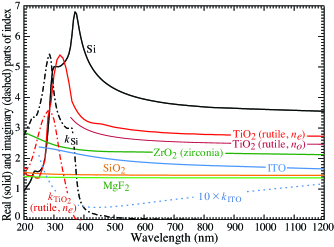
The indices of silicon and some candidate AR films are shown in Fig. 3. Indices of the transparent films (TiO2, ZrO2, HfO2, fused SiO2, MgF2, etc.) are widely tabulated for bulk samplesfil , but must be used with caution, especially for sputtered or vapor-deposited films. For our application HfO2 is inferior to ZrO2. SiO2 and MgF2 have very similar properties, but since the LBNL MicroSystems Lab has wide experience with SiO2 films, it is used in preference to MgF2. With the exception of SiO2, Si, ISDP, and all of the AR films used present special problems that are discussed here.
More extensive studies of candidate materials have been published by Smith & BaumeisterSmith and Baumeister (1979) and by LesserLesser (1987), focussing on UV transparent oxides and fluorides.
III.1 Index of silicon
While the coatings and boundary conditions at the surfaces of the CCD affect transmission and reflection, it is absorption in the silicon substrate that results in charge collection. Understanding is therefore of paramount importance in understanding its QE. This is particularly true in the near infrared, where the the absorption length rapidly approaches the thickness of the silicon substrate as the indirect bandgap is approached (at 1.12 eV, or 1100 nm, depending on temperature), reducing the QE to nearly zero.
Many papers over the last 60 years have been devoted to the refractive index of silicon, particularly the absorptive part, because of its great importance in solar cell design. A subset of these studies is particularly relevant to the optical and near-IR response of a CCDGreen (2008); Rajkanan et al. (1979); Macfarlane et al. (1958); Dash and Newman (1955); Philipp and Taft (1960); Weakliem and Redfield (1979); Jellison and Modine (1982a, b); Jellison and Burke (1986); Jellison (1992); Bücher et al. (1994); Green and Keevers (1995). Two of these are relevant to our studies:
-
1.
GreenGreen (2008) (2008) published tables of optical parameters at K, together with empirical power-law temperature coefficients for , , and 333To maintain the required significance at longer wavelengths it is necessary to recalculate from Green’s absorption coefficients. Tables are most easily copied from the web version: sciencedirect.com/science/article/pii/S0927024808002158# : “The self-consistent tabulation was derived from Kramers-Kronig analysis of updated reflectance data deduced from the literature.” Our earlier workGroom et al. (1999) used values of from the Handbook of Optical Constants of SolidsEdwards (1985) extended to 1100 nm via tables presented by JanesickJanesick (iven). Green’s values are quite close to these, but in our view supersede them.
Temperature coefficients “calculated from cited and additional data sets” describe simple power laws as given in his Eqs. (9) and (10). Calculations using these coefficients indicate that the real part of the index varies only weakly with temperature. Changes are most evident near 380 nm. Since Green’s K) and K) are nearly indistinguishable, we have adopted Green’s K) for model calculations at all temperatures.
Absorption calculated using his coefficients yields model QE’s seriously at variance with our data. An example is shown in Fig. 11.
-
2.
Rajkanan et al.Rajkanan et al. (1979) (1979) developed a physics-based model of the absorption that used experimental data from MacFarlane et al.Macfarlane et al. (1958) and unpublished NASA sources to determine model parameters444A nearly-identical expression for is given by Bücher et al.Bücher et al. (1994) without reference to Rajkanan et al.’s earlier paper. With two exceptions, the parameters are the same or nearly the same. However, the direct allowed bandgap contribution is given as , rather than Rajkanan et al.’s . Evidently the exponent should be 1/2 for a direct bandgap transitionPankove (1971). Although both forms give similar results for photon energies below , we choose Rajkanan et al.’s form.. The best accuracy was obtained “with indirect band gaps at 1.1557 and 2.5 eV and a direct allowed gap at 3.2 eV” (390 nm).
A fairly abrupt change in the absorption coefficient as the photon energy crosses this threshold (which increases somewhat with temperature) is evident in Fig. 2. Although their paper implies only 20% accuracy, we find remarkable agreement between the model predictions and our measured CCD QE at different temperatures and substrate thicknesses. At wavelengths below 390 nm, the Rajkanan et al. curves differ somewhat from measured values. This is due to the simple, smooth curve for obtained from the Rajkanan et al. model in the direct bandgap region. It makes little practical difference, since (a) our QE measurements extend down only to 320 nm, and (b) absorptions lengths are so short (a few 10’s of nm) that the ISDP layer already confuses the issue.
Satisfactory agreement between QE modeled using the Rajhanan et al.’s absorption coefficientRajkanan et al. (1979) and data is obtained in all cases for the fiducial region in which the QE drops from 90% to 20% of its maximum, spanning a CCD thickness range from 200 m to 500 m and temperature range from 20∘ C to 140∘ C. A surprising low-energy “skirt” at the higher temperatures extending the QE well above the indirect bandgap energy is discussed in connection with the TiO2/SiO2 coated CCD’s.
III.2 Index of in-situ doped polysilicon (ISDP)
During fabrication, a fairly thick layer of phosphorus-doped polycrystalline silicon on the rear surface of the CCD acts as an active getter, maintaining the necessary very low leakage currents through high-temperature processing steps. After thinning and polishing a backside ohmic contact is formed by depositing a thin ISDP layer (10–25 nm). The process is described in more detail in Ref. Holland et al., 2003. Also shown in that paper is a secondary ion mass spectroscopy depth profile of a nominal 20 nm thick ISDP layer. The P concentration varies by a factor of three until a depth of 20 nm is reached, then drops exponentially at about one decade/7 nm. It is difficult to convert this profile to a single number for model calculations. In most cases the model thickness needs to be increased by 5–10 nm from the nominal value to obtain agreement with measurements.
The real part of its index is about the same as that of silicon, but it is considerably more absorptive than silicon in the blueLubberts et al. (1981). Tables SIPOLY.NK in the SOPRA databasefil provide and for = 10–90. The peak values of both and decrease as increases. Documentation of the SOPRA tables is not available, but it is likely that is the fraction (in %) of amorphous silicon present. For nm rises slightly with , while increases significantly.
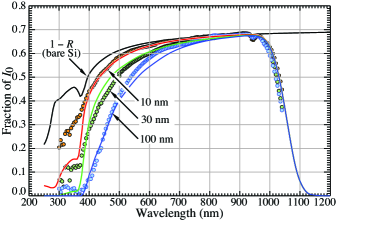
Holland, Wang, and Moses fabricated and measured the QE of a series of photodiodes with successively thicker ISDP coatingsHolland et al. (1997). A sample of their data together with model fits using SIPOLY10.NK are shown in Fig. 4 for ISDP thicknesses of 10, 30, and 100 nm. In the 10 nm case the data and model are in essential agreement above 390 nm. The agreement is worse for the 30 and 100 nm cases, but the disagreement is in different directions. In all cases, and in our CCD QE measurements, the model QE falls below data for nm; our assumed index is simply too absorptive in this region. Since the QE is already falling rapidly here, the error is of little practical consequence.
In the model QE calculations, ISDP absorption peaks at about 350 nm, and falls to insignificance in the red. Since there are yield concerns if the ISDP is too thin, most recent CCD’s use 25 nm coatings at the expense of significant QE loss below 500 nm.
III.3 Index of indium-tin oxide (ITO)
ITO films are (nearly) transparent to visible and near-IR light. In spite of ITO’s widespread use, it is not an optically invariant material. Its optical properties depend upon the method of application, temperature, pressure, sputtering atmosphere and power, composition, and annealing. It varies from amorphous to crystalline, and often has a graded indexWoollam et al. (1994); Gerfin and Grätzel (1996); Lee et al. (1993); Rhaleb et al. (2002); Guillén and Herrero (2007).
ITO was first used in our application to augment rear surface conductivity and also, with careful thickness choice, to act as an AR coating or first layer of an AR coatingHolland et al. (1997). It was reactively sputtered at room temperature in a low-pressure O2/Ar atmosphere from a target composed of 90% In2O3 and 10% SnO2 by weight. To optimize conduction in the ITO, the oxygen content of the film (less than saturated) was controlled using deposition parameters described in Ref. Holland et al., 1997. Annealing in N2 for an hour at 200∘ C substantially improved the transmittance.
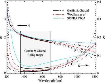
Our original sources of information about the optical constants for indium-tin oxide were the papers by Woollam, McGahan, & JohsWoollam et al. (1994) and Gerfin & GrätzelGerfin and Grätzel (1996). Reference Gerfin and Grätzel, 1996 gives tables of 6-parameter fits to a dispersion formula for the dielectric constant . Figure 5 shows the index, calculated as the real part of , for three ITO films obtained from different sources. The Gerfin & Grätzel fits are based on data for nm. Data from a figure in Ref. Woollam et al., 1994 as smoothed by Gerfin & Grätzel’s dispersion formula are shown by the dash-dotted red lines, the basis of our modeling calculations until recently. The curvature change and decrease of the index above 700 nm are expected from Drude-type absorption, indicating free carriers in the film. The solid magenta curves 250–850 nm are from ITO2.NK in the SOPRA database. The SOPRA indices, linearly extrapolated to nm, have been used recently, and provide somewhat better agreement with the measured QE. Since the dispersion fits show increasing slope of with and decreasing slope of with , the SOPRA data and in particular our linear extrapolation may be unphysical. Attempts to fit a Gerfin & Grätzel-style dispersion function to the SOPRA data have failed to converge. Index uncertainties in the extrapolated region are relatively unimportant in our application.
III.4 Index of zirconium oxide
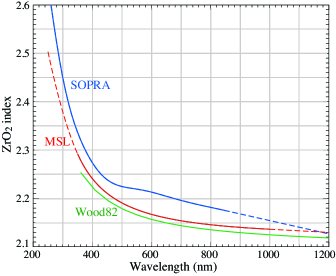
The refractive index of ZrO2 from three sources is shown in Fig. 6. The SOPRA datafil show a curious inflection at about 600 nm, perhaps from combining indices from different sources. The LBNL MicroSystems Lab (MSL) sputtered film spectroscopic ellipsometer measurements were made at the LBNL Molecular Foundry. The cubic zircona sample measured by Wood & NassauWood and Nassau (1982) contained 12-mole % yttria. Since the index of Y2O5 is considerably lower than that of ZrO2Nigara (1968), one might expect the Wood & Nassau sample to have a smaller index than pure ZrO2, as the figure suggests.
The MSL and Wood & Nassau curves have roughly the same smooth shape, without the unexpected structure near 600 nm. We use the MSL index for our calculations.
III.5 Index of titanium dioxide
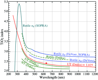
The index of the rutile form of TiO2 shown in Fig. 3 (highest curve) is from SOPRA TIO2.NK, and tables are available through Filmetricsfil . It may have the highest index for any transparent AR film candidate. Its wavelength dependence is remarkably similar to that of silicon, making it the near-ideal material for a wideband antireflective coating. But there are problems: the SOPRA TIO2.NK index is evidently for the extraordinary ray in this birefringent materialDeVore (1951); Edwards (1985). Moreover, reactively sputtered TiO2 films at temperatures consistent with CCD fabrication are mostly the (also birefringent) anatase form: “Annealing of the films in air at 850 ∘C showed that anatase-rutile transformation strongly depends on the deposition temperature; the films deposited at temperature below 400∘C were converted to the anatase-rutile mixture films, and the films deposited at 400∘C to complete rutile films”Wicaksana et al. (1992). The index of anatase is considerably below that of rutile, and tables are not readily available. The many papers on the subject do not present consistent resultsDakka et al. (1999); Tang et al. (1994); R. Dannenberg (2000); Jellison et al. (2003); Miao et al. (2003). For example, Dakka et al.Dakka et al. (1999) show different indices for “new target” (NT) and “used target” (UT) samples, and describe porosity and voids. The Dakka et al. results, together together with DeVoreDeVore (1951) and SOPRAfil indices, are shown in Fig. 7.
III.6 “Index” of the mechanical substrate
When transmission becomes important in the near IR ( nm, depending on the thickness of the silicon), the light exits into the gate structure and a mechanical substrate, which we have often modeled as exit into air: . It is is considerably more complicated than this, as shown in Fig. 1. The light encounters 50 nm of SiO2, then 50 nm of Si3N4, polysilicon gates 300 nm thick (with 40% overlap), a thick layer of SiO2, and epoxy that binds the device to thick silicon or aluminum nitride. Remarkably, a single index seems to describe this region adequately. Modeled QE turns out to be very insensitive to its value: or even moves the model calculation in the steep IR falloff region only slightly to the left, where it agrees slightly better with the measurements. However, asymptotic 1 and increase significantly with increasing . Examples are shown below for both and .
IV Model calculations compared with QE and reflectivity measurements
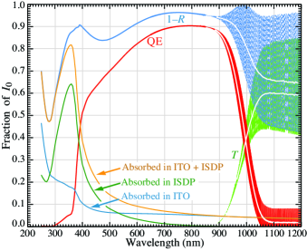
Only the reflectivity and the transmitivity are directly modeled. As per the discussion of Sec. II, can be approximately decomposed into the QE, the light fraction absorbed in the ISDP layer (), and the fraction absorbed in the antireflective coatings (). If the AR coating is not significantly absorptive, the QE and 1 curves should be nearly identical for a fairly wide region in the red and near IR, where there is no transmission and the ISDP is essentially transparent. If the AR coating does absorb significantly at all wavelengths, then there is a calculable gap between the QE and 1 curves, as is evident in Figs. 9 and 10. The measured QE is subject to amplifier gain uncertainties and other problems at the few-percent level. The absolute measurement of is used to normalize the QE measurements.
The QE can be measured in either the normal CCD mode or by reading out the entire or a masked subsection of the CCD as a photodiode (PD mode). This provides some additional redundancy, and measurements can be made at higher temperatures than are possible in the CCD mode. An example is discussed in Sec. IV.4.
Our setup for measuring the QEGroom et al. (2006) is fairly standard: light from a monochromator enters an integrating sphere and exits a large aperture. It arrives at the dewar containing the CCD after an 0.8 m drift space in a baffled box. Slit widths are varied with light intensity; the bandwidth can be as small as 10 nm. A room-temperature standard photodiode at the CCD’s position and behind the same dewar window is used to calibrate a similar photodiode at a small port in the integrating sphere that is then used as the reference for the QE measurement.
The reflectometer is described in Ref. Fabricius et al., 2006. The intensity of a light beam from the monochromator is measured by a photodiode after several mirror reflections. One mirror is then moved so that a reflection from the (air-backed) CCD wafer sample is included in the optical path. The ratio yields the absolute reflectivity . These measurements are at room temperature.
The CCD’s have from 4 to 16 readout amplifiers whose gain calibrations can be uncertain at the few percent level. In a broad red spectral band the QE should be nearly 1; this is used to normalize the QE measurements.
The CCD’s fabricated and studied so far use various combinations of ISDP, ITO, ZrO2, TiO2, and SiO2 films on the silicon substrate. While the index of SiO2 is very well known, the others all require special attention. In particular, the near IR response of the CCD depends crucially on the absorption coefficient of silicon, which is discussed in detail.
IV.1 Two-layer AR coating design methodology
Recent designs use a minimal-thickness ITO coating over the ISDP, followed by high-index and low-index layers. Although this is technically a 3-layer AR coating, the thickness of the ITO is held constant in optimizing the other thicknesses for maximum response.
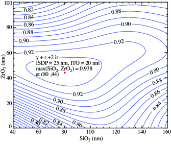
In the absence of any clear criterion for AR coating optimization, the response was maximized for several linear combinations of broadband and narrowband filter responses. Figure 8 shows an example for an ITO (fixed 20 nm thick)/ZrO2/SiO2 coating, where the model QE is the average of HSC-g and HSC-i responsesHSC . Response was calculated for a matrix of ZrO2 and SiO2 thicknesses to make the QE contour plot. Thickness tolerances can be estimated from the “flatness” of the peak.
Although still somewhat subjective, the method has been moderately successful. Subsequent thickness tuning on the basis of experiment has also been useful. One problem, still not understood, is a discrepancy of 10–15% between the deposited SiO2 thickness and the modeled thickness—the CCD behaves as though excessive SiO2 has been deposited555Blacksberg et al. report measured film indices somewhat different than were expectedBlacksberg et al. (2008). For SiO2 they find a film index about 2% higher than for bulk fused quartz, in the right direction but not enough to explain our apparent excess. . We correct for this empirically by depositing a thinner SiO2 layer.
IV.2 ITO/SiO2 coating
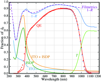
In initial designs, indium-tin oxide was used both to ensure adequate rear-surface conductivity and to serve as the first layer of the AR coating. The model output is shown in Figs. 9, 10, and 13. The full calculation is shown in Fig. 9. In this and in most other examples, light is normally incident on the CCD. The decomposition of the absorption into QE, absorption in the ISDP+AR coating, ISDP, and AR is discussed in Sec. II. Above 900 nm the CCD becomes increasingly transparent, resulting in interference between the reflected and transmitted amplitudes in the silicon substrate. The responses change rapidly with increasing wavelength, and appear as bands in Fig. 9. White lines show box-car averaged , 1, and QE, the intensity fraction absorbed in the sensitive region. The discrepancy between 1 and the QE in the near-IR is primarily caused by absorption in the ITO. The approximations made in separating the QE and absorption in the ISDP and ITO break down as fringing becomes more pronounced, so the modeled QE does not quite go to zero at long wavelengths.
Figure 10 shows the same curves, but with the fringing bands replaced by boxcar averages, experimental QE measurements (red triangles) added, and a dashed curve comparing the modeled 1 with results from the Filmetrics Reflectivity Calculatorfil has been added. Blue circles on the descending part of the QE response illustrate a correction for the finite monochromator bandpass.
For this model calculation , the effective index of the mechanical substrate, , was taken as 1.00. The value is relevant only in the transparency region, nm.
IV.3 (ITO)/ZrO2/SiO2 coating
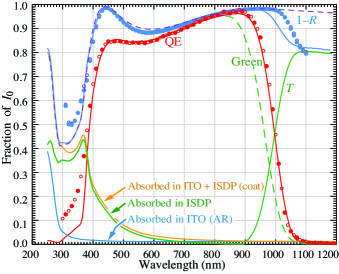
A design has been developed for the Dark Energy Spectroscopic Instrument (DESI)Bebek et al. (2015) that uses ZrO2 rather than ITO for most of the high-index layer. There is a 20–25 nm ITO film between the ISDP and ZrO2. The ITO is included to avoid direct contact with a new material that might introduce reliability issues. (We have had substantial experience with ITO in direct contact with ISDP.) In any case, the ITO does not seriously compromise the QE in the DESI red and IR channelsBebek et al. (2015). An example is shown in Fig. 11. Compared with the ITO/SiO2 response (Figs. 9 and 10), the blue QE is increased and flattened, and the QE is only slightly below the 1 limit in a broad red region.
For the model calculation shown here, , the effective index of the mechanical substrate, was taken as 1.50. A comparison with Fig. 9, where it was 1.00, shows that the asymptotic transparency and 1 are both greater, although their difference (nearly the QE in this case) is almost unchanged.
The near-IR QE using Green’s Green (2008) (Sec. III.1) is also shown in Fig. 11. Green’s agreement with Rajkanan et al. is better when the comparison is made at C.
IV.4 TiO2/SiO2 coating
Since the LBNL MicroSystems Lab did not have a sputtering target for TiO2 deposition, a TiO2/SiO2 coating was applied to an otherwise-complete CCD by the Hionix corporationhio . They reported a TiO2 index of 2.44 at 633 nm. The SiO2 film was about 14% thicker than requested, resulting in a QE somewhat lower than expected.
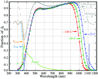
The response is shown in Fig. 12. Good fits to the measured QE were obtained using the Dakka “UT” index scaled by 1.025, in agreement with the Hionix measurement at 633 nm. This CCD has a better response than any of the others we have tested. Nonetheless, given the difficulty and likely unpredictability of TiO2 films and only marginal improvement from the (ITO)/ZrO2/SiO2 AR coating, there is little incentive to pursue this approach.
A remarkable feature of the room-temperature measurements is the QE “skirt” extending well beyond 1116 nm, the wavelength corresponding to the indirect bandgap at 1.1108 eV at 300∘K (vertical dotted line in Fig. 12). In order to conserve both energy and momentum, absorption involving indirect transitions requires the absorption or emission of one or more phonons. The Rajkanan et al. modelRajkanan et al. (1979) takes into account the two lowest phonon excitations, 0.0183 eV and 0.0577 eV that produce contributions to the absorption coefficient with displacements of nm and nm. As a result, the model QE at 25∘ C shown in Fig. 12 is about 8% at 1100 and falls to zero by 1177 nm. However, the measured response is above 10% at 1120 nm and falls to zero only just below 1200 nm. This e-h production by low-energy photons is thought to be due to higher-temperature double-phonon processes producing offsets of nm and nmMacfarlane et al. (1958).
IV.5 Fringing
The sensitive region of a “traditional” thin back-illuminated CCD is an epitaxial layer 20 m thick. At longer wavelengths light reaches the back surface, and the resulting multiple reflections produce interference “fringes.” A white-light exposure with the KECK low-resolution spectrograph (LRIS)Oke et al. (1995) is shown in Ref. Groom et al., 1999. The fringes are somewhat irregular because of thickness variations in the epitaxial layer, but one can infer from the fringe average spacing that the layer is 20–22 m thick. (For a thickness at a wavelength where the real part of the silicon index is , .) In this case, the spacing is about 7 nm at nm, providing at once a way to measure the epitaxial layer thicknessJanesick (2001) and a nuisance for observers. Broadband photometry using R and IR filters is plagued by swirled interference patterns whose amplitude is modulated by time-varying OH sky lines. Removal of these fringes is discussed by McLeanMcLean (1997) and others, and algorithms to treat the problem are part of observatory software. That the fringes exist means that the light remains coherent over at least 20 m and that reflection from the mechanical substrate is remarkably specular.
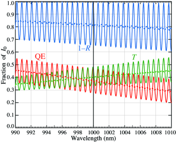
An expansion of our modeled 990–1100 nm region for a 200 m thick CCD’s is shown in Fig. 13. For normally incident light the peak-to-valley QE variation is nearly 0.2 of the incident intensity, or 0.34 of the average QE. However, the fringes are ten times closer than those in a 20 m thick CCD, or about 0.7 nm at 1000 nm. Only the highest-resolution spectrometers could resolve these fringes. In particular, they are not resolved in our QE measurements because of the much-wider bandpass of the monochromator. Even if they are not observed, the agreement of the boxcar averaged QE with measured QE argues for coherence and fairly specular reflection.
An actual instrument has a finite aperture, so that light arrives at different angles, each with a fringe spacing characteristic of the slant depth. The fringing pattern tends to average out. The central dashed lines in Fig. 13 were calculated for an f1.5 aperture. The remaining oscillations are the result of a beat pattern characteristic of this wavelength range; in the model they disappeared and reappeared as the aperture was changed. Results of the calculation are nearly independent of polarization.
Using a DECam CCD, Stevenson et al.Stevenson et al. (2016) searched for water in the atmosphere of an exoplanet with the LDSS-3 spectrometer (focal ratio f2.5) at the Magellan telescope at Las Campanas Observatory. Fringes were not observed. A more detailed study of one of the images by A. Seifahrtsei (2016) set limits on the fringe intensity of 0.25% (peak-to-valley).
DECcam Y-band images have shown fringing swirls at the 0.4% peak-to-valley levelmar . The pattern and spacing is probably inconsistent with interference in the CCD itself, given its thickness and expected thickness variations. It is possible that the interference originates in the epoxy layer binding the CCD to the mechanical substrate, which was aluminum nitride for the DECam CCD’s.
In any case, the steep QE falloff in the near IR limits any possible fringing to the 900–1050 nm region. The fringing amplitude, especially in the cases of the DESI (ITO)/ZrO2/SiO2 CCD(Fig. 11) and the TiO2/SiO2 CCD (Fig. 12), is minimized by the very low reflectivity in this region. For normally incident light the maximum peak-to-valley QE variation is 0.10 for the DESI CCD and 0.08 for the TiO2/SiO2 CCD.
V Prospects for QE improvement
It was mentioned above that the model thicknesses had to be “tuned” somewhat to obtain agreement with the measurements. To some extent this was because of variation in the actual film thicknesses, or, more likely, that the thin film indices were different from those measured in bulk samples. (In the case of TiO2, there was even ambiguity about the crystal form.) Thus by perturbing the actual film thicknesses the QE can be improved. Experimental AR coatings are being made to explore this. It is likely that response of the (ITO)/ZrO2/SiO2 (DESI) CCD can be enhanced in the 450–600 nm region from about 84% to about 90% by increasing the design ZrO2 thickness by 7–10 nm—a spectral region just below the DESI red channel, but the increased blue response might be useful for other applications.
Our blue response is limited by absorption in the ISDP rear electrode. An alternate approach is delta doping, depositing approximately a monolayer of dopant atoms on the rear surface via molecular beam epitaxy (MBE). This technique has been developed at the Jet Propulsion Lab (Caltech) for a variety of spacecraft and sounding rocket missionsNikzad et al. (2016). The object is to obtain reflection-limited ultraviolet quantum efficiency down to about 100 nm.
Antimony layers about 5 nm thick were applied in this way to 2k4k and 1k1k LBNL CCD’s similar to those described hereBlacksberg et al. (2008); Jacquot et al. (2010). QE measurements with and without a (nominally) Si3N4/SiO2 AR coating are shown in Ref. Blacksberg et al., 2008. The results are consistent with ours except that their QE remains high down to about 400 nm.
There has been no further work on the delta-doping approach.
VI Conclusions
We have extended standard thin-film optics methods to model the quantum efficiency (QE) of LBNL thick, back-illuminated CCD’s, and compared the results with experimental measurements of QE and reflectivity for three antireflective coating examples. The calculations included (a) considering the thick substrate as one of the films and (b) separating absorption in an ISDP coating serving as the rear contact and in the antireflective coating from absorption in the silicon substrate (the QE) by modifying boundary conditions. Problems encountered with the indices involved are discussed. While agreement with experimental QE and reflectivity measurements are regarded as adequate, it is limited by uncertainties in the ISDP index, the ITO and TiO2 indices, and film deposition thickness variations. Fringing is neither expected nor observed.
VII Acknowledgements
The QE “machine” was built by Jens Stecker and the reflectometer by Maximilian Fabricius, both in collaboration with and under the supervision of Armin Karchar. With the exception of TiO2, AR coatings were applied in the LBNL MicroSystems Lab. We are also grateful for Chris Bebek’s encouragement and guidance. .
This work was supported by the U.S. Department of Energy under Contract No. DE-AC02-05CH11231.
References
- Holland et al. (2003) S. Holland, D. Groom, N. Palaio, R. J. Stover, and M. Wei, in IEEE Trans. Electron Devices, Vol. 50 (2003) pp. 225–238.
- Holland et al. (2006) S. E. Holland, C. J. Bebek, K. S. Dawson, J. H. Emes, M. H. Fabricius, J. A. Fairfield, D. E. Groom, A. Karcher, W. F. Kolbe, N. P. Palaio, N. A. Roe, and G. Wang, in Society of Photo-Optical Instrumentation Engineers (SPIE) Conference Series, Proc. SPIE, Vol. 6276 (2006) p. 62760B.
- Groom et al. (1999) D. E. Groom, S. E. Holland, M. E. Levi, N. P. Palaio, S. Perlmutter, R. J. Stover, and M. Wei, in Sensors, Cameras, and Systems for Scientific/Industrial Applications, Proc. SPIE, Vol. 3649, edited by M. M. Blouke and G. M. Williams (1999) pp. 80–90.
- Edwards (1985) D. F. Edwards, Handbook of Optical Constants of Solids, edited by E. D. Palik (Academic Press, 1985) pp. 547–569.
- Janesick (iven) J. R. Janesick, IS&T/SPIE Symposium on Electronic Imaging Science and Technology , 233 (no data source or year given).
- Green (2008) M. A. Green, Solar Energy Materials and Solar Cells 92, 1305 (2008).
- Rajkanan et al. (1979) K. Rajkanan, R. Singh, and J. Shewchun, Solid-State Electronics 22, 793 (1979).
- Pedrotti and Pedrotti (1993) F. L. Pedrotti and L. S. Pedrotti, Introduction to Optics (Prentice Hall, New Jersey, 1993).
- Hecht (1998) E. Hecht, Optics, 3rd ed. (Adddison-Wesley, 1998).
- Macleod (2001) H. A. Macleod, Thin-Film Optical Filters, 3rd ed. (Institute of Physics, Bristol, 2001).
- Jenkins and White (1950) F. A. Jenkins and H. E. White, Fundamentals of Optics (2nd edition) (McGraw Hill, New York, 1950).
- Panofsky and Phillips (1955) W. K. Panofsky and M. Phillips, Classical Electricity and Magnetism (Addison-Wesley, Redding, MA, 1955).
- Slater and Frank (1947) J. C. Slater and N. H. Frank, Electromagnetism (McGraw-Hill, New York, 1947).
- Born and Wolf (1999) M. Born and E. Wolf, Principles of Optics, 7th ed. (Pergamon, Cambridge, 1999).
- Sommerfeld (1964) A. Sommerfeld, Optics (Academic Press, New York, 1964).
- (16) Most useful indices can be downloaded from filmetrics.com. Many are from the SOPRA Material Database, given without citation. In some cases polynomial or dispersion fits can be found.
- Smith and Baumeister (1979) D. Smith and P. Baumeister, Applied Optics 18, 111 (1979).
- Lesser (1987) M. Lesser, Optical Engineering 26, 911 (1987).
- Macfarlane et al. (1958) G. G. Macfarlane, T. P. McLean, J. E. Quarrington, and V. Roberts, Phys. Rev. 111, 1245 (1958).
- Dash and Newman (1955) W. C. Dash and R. Newman, Phys. Rev. 99, 1151 (1955).
- Philipp and Taft (1960) H. R. Philipp and E. A. Taft, Phys. Rev. 120, 37 (1960).
- Weakliem and Redfield (1979) H. A. Weakliem and D. Redfield, J. App. Phys. 50, 1491 (1979).
- Jellison and Modine (1982a) G. E. Jellison, Jr. and F. A. Modine, J. App. Phys. 53, 3745 (1982a).
- Jellison and Modine (1982b) G. E. Jellison, Jr. and F. A. Modine, Appl. Phys. Lett. 41, 180 (1982b).
- Jellison and Burke (1986) G. E. Jellison, Jr. and H. H. Burke, J. App. Phys. 60, 841 (1986).
- Jellison (1992) G. E. Jellison, Optical Materials 1, 41 (1992).
- Bücher et al. (1994) K. Bücher, J. Bruns, and H. G. Wagemann, J. App. Phys. 75, 1127 (1994).
- Green and Keevers (1995) M. A. Green and M. Keevers, Progress in Photovoltaics 3, 189 (1995).
- Note (1) To maintain the required significance at longer wavelengths it is necessary to recalculate from Green’s absorption coefficients. Tables are most easily copied from the web version: sciencedirect.com/science/article/pii/S0927024808002158#.
- Note (2) A nearly-identical expression for is given by Bücher et al.Bücher et al. (1994) without reference to Rajkanan et al.’s earlier paper. With two exceptions, the parameters are the same or nearly the same. However, the direct allowed bandgap contribution is given as , rather than Rajkanan et al.’s . Evidently the exponent should be 1/2 for a direct bandgap transitionPankove (1971). Although both forms give similar results for photon energies below , we choose Rajkanan et al.’s form.
- Lubberts et al. (1981) G. Lubberts, B. C. Burkey, F. Moser, and E. A. Trabka, J. Appl. Phys. 52, 6870 (1981).
- Holland et al. (1997) S. E. Holland, N. W. Wang, and W. W. Moses, IEEE Trans. Nucl. Sci. 44, 443 (1997).
- Woollam et al. (1994) J. A. Woollam, W. A. McGahan, and B. Johs, Thin Solid Films 241, 44 (1994).
- Gerfin and Grätzel (1996) T. Gerfin and M. Grätzel, J. Appl. Phys. 79, 1722 (1996).
- Lee et al. (1993) S. B. Lee, J. C. Pincenti, A. Cocco, and D. L. Naylor, J. Vac. Sci. Tech. A 11, 2742 (1993).
- Rhaleb et al. (2002) H. E. Rhaleb et al., Applied Surface Science 201, 138 (2002).
- Guillén and Herrero (2007) C. Guillén and J. Herrero, J. App. Phys. 101, 073514 (2007).
- Wood and Nassau (1982) D. L. Wood and K. Nassau, Appl. Optics 21, 2978 (1982).
- Nigara (1968) Y. Nigara, Jpn. J. Appl. Phys. 7, 404 (1968).
- DeVore (1951) J. R. DeVore, J. Opt. Soc. Am. 41, 416 (1951).
- Wicaksana et al. (1992) D. Wicaksana, A. Kobayashi, and A. Kinbara, J. Vac. Sci. Technol. A 10, 1479 (1992).
- Dakka et al. (1999) A. Dakka, J. Lafait, M. Abd-Lefdil, and C. Sella, M.J.Condensed matter 2, 153 (1999).
- Tang et al. (1994) H. Tang, H. Berger, P. Schmid, and F. Levy, Solid State Communications 92, 267 (1994).
- R. Dannenberg (2000) P. G. R. Dannenberg, Thin Solid Films 360, 122 (2000).
- Jellison et al. (2003) G. E. Jellison et al., J. Appl. Phys. 93, 9537 (2003).
- Miao et al. (2003) L. Miao, P. Jin, K. Kaneko, A. Terai, N. Nabatova-Gabain, and S. Tanemura, App. Surface Sci. 212-213, 255 (2003).
- Groom et al. (2006) D. E. Groom, C. J. Bebek, M. Fabricius, A. Karcher, W. F. Kolbe, N. A. Roe, and J. Steckert, in Sensors, Cameras, and Systems for Scientific/Industrial Applications VII, Proc. SPIE, Vol. 6068, edited by M. M. Blouke (2006) pp. 133–143.
- Fabricius et al. (2006) M. H. Fabricius, C. J. Bebek, D. E. Groom, A. Karcher, and N. A. Roe, in Sensors, Cameras, and Systems for Scientific/Industrial Applications VII, Proc. SPIE, Vol. 6068, edited by M. M. Blouke (2006) pp. 144–154.
- (49) S. Kawanomoto et al., in prep.
- Note (3) Blacksberg et al. report measured film indices somewhat different than were expectedBlacksberg et al. (2008). For SiO2 they find a film index about 2% higher than for bulk fused quartz, in the right direction but not enough to explain our apparent excess.
- Smee et al. (2013) S. A. Smee, J. E. Gunn, A. Uomoto, N. Roe, D. Schlegel, et al., Astron. J. 146, 32 (2013).
- Flaugher et al. (2015) B. Flaugher, H. T. Diehl, K. Honscheid, et al., Astron. J. 150, 150 (2015), arXiv:1504.02900 .
- Rockosi et al. (2010) C. Rockosi, R. Stover, et al., in Ground-based and Airborne Instrumentation for Astronomy III, SPIE, Vol. 7735 (2010) p. 77350R.
- Bebek et al. (2015) C. Bebek, J. Emes, D. Groom, S. Haque, S. Holland, A. Karcher, W. Kolbe, J. Lee, N. Palaio, and G. Wang, J. Instr. 10, C05026 (2015).
- (55) Hionix, Inc., hionix.com.
- Pankove (1971) J. I. Pankove, Optical processes in semiconductors (Dover Publications, New York, 1971) pp. 36–42.
- Oke et al. (1995) J. B. Oke et al., P. A. S. P. 107, 375 (1995).
- Janesick (2001) J. R. Janesick, Scientific charge-coupled devices, Bellingham, WA: SPIE Optical Engineering Press, 2001, xvi, 906 p. SPIE Press monograph, PM 83 (2001).
- McLean (1997) I. S. McLean, ed., Electronic imaging in astronomy. Detectors and instrumentation (UK Wiley, Chichester, 1997).
- Stevenson et al. (2016) K. B. Stevenson, J. L. Bean, A. Seifahrt, et al., Astrophys. J. 817, 141 (2016), arXiv:1511.08226 .
- sei (2016) Andreas Seifahrt (Univ. of Chicago), personal communication (2016).
- (62) P. Martini (Ohio State Univ.), personal communication (2012).
- Nikzad et al. (2016) S. Nikzad, A. D. Jewell, M. E. Hoenk, T. Jones, J. Hennessy, T. Goodsall, A. Carver, C. Shapiro, S. R. Cheng, E. Hamden, G. Kyne, D. C. Martin, D. Schiminovich, P. Scowen, K. France, S. McCandliss, and R. E. Lupu, ArXiv e-prints (2016), arXiv:1612.04734 [astro-ph.IM] .
- Blacksberg et al. (2008) J. Blacksberg, S. Nikzad, M. E. Hoenk, S. E. Holland, and W. F. Kolbe, IEEE Transactions on Electron Devices 55, 3402 (2008).
- Jacquot et al. (2010) B. C. Jacquot, S. P. Monacos, T. J. Jones, J. Blacksberg, M. E. Hoenk, and S. Nikzad, in High Energy, Optical, and Infrared Detectors for Astronomy IV, Proc. SPIE, Vol. 7742 (2010) p. 77420I.