Electrically driven electron spin resonance mediated by spin-valley-orbit coupling in a silicon quantum dot111Published on npj Quantum Information 4,6 (2018), doi:10.1038/s41534-018-0059-1. License CC BY 4.0
The ability to manipulate electron spins with voltage-dependent electric fields is key to the operation of quantum spintronics devices such as spin-based semiconductor qubits. A natural approach to electrical spin control exploits the spin-orbit coupling (SOC) inherently present in all materials. So far, this approach could not be applied to electrons in silicon, due to their extremely weak SOC. Here we report an experimental realization of electrically driven electron-spin resonance in a silicon-on-insulator (SOI) nanowire quantum dot device. The underlying driving mechanism results from an interplay between SOC and the multi-valley structure of the silicon conduction band, which is enhanced in the investigated nanowire geometry. We present a simple model capturing the essential physics and use tight-binding simulations for a more quantitative analysis. We discuss the relevance of our findings to the development of compact and scalable electron-spin qubits in silicon.
I Introduction
Silicon is a strategic semiconductor for quantum spintronics, combining long spin coherence and mature technology Zwanenburg13 . Research on silicon-based spin qubits has seen a tremendous progress over the past five years. In particular, very long coherence times have been achieved with the introduction of devices based on the nuclear-spin-free 28Si isotope, enabling the suppression of hyperfine coupling, the main source of spin decoherence Tyryshkin12 . Single qubits with fidelities exceeding 99% as well as a first demonstration of a two-qubit gate have been reported Veldhorst14 ; Laucht15 ; Veldhorst15b .
finding a viable pathway towards large-scale integration is the next step. To this aim, access to electric-field-mediated spin control would facilitate device scalability, circumventing the need for more demanding control schemes based on magnetic-field-driven spin resonance. Electric-field control requires a mechanism coupling spin and motional degrees of freedom. This so-called spin-orbit coupling (SOC) is generally present in atoms and solids – due to a relativistic effect, electrons moving in an electric-field gradient experience in their reference frame an effective magnetic field. In the case of electrons in silicon, however, SOC is intrinsically very weak.
Possible approaches to circumvent this limitation have so far relied either on the introduction of micromagnets, generating local magnetic field gradients and hence an artificial SOC Pioro-Ladriere08 ; Kawakami14 ; Rancic16 ; Takeda16 , or on the use of hole spins Maurand16 , for which SOC is strong. In both cases, relatively fast coherent spin rotations could be achieved through resonant radio-frequency (RF) modulation of a control gate voltage. While the actual scalability of these two solutions remains to be investigated, other valuable opportunities may emerge from the rich physics of electrons in silicon nanostructures Nestoklon06 ; Zwanenburg13 ; Hao14 ; Schoenfield17 ; Jock17 ; Veldhorst15 ; Ruskov2017 .
Silicon is indeed an indirect band-gap semiconductor with six degenerate conduction-band valleys. This degeneracy is lifted in quantum dots (QD) where quantum confinement leaves only two low-lying valleys that can be coupled by potential steps at Si/SiO2 interfaces. The resulting valley eigenstates, which we label and , are separated by an energy splitting ranging from a few tens of eV to a few meV Sham79 ; Saraiva09 ; Friesen10 ; Culcer10 . depends on the confinement potential, and can hence be tuned by externally applied electric fields Goswami07 ; Yang13 ; Laucht15 . Even if weak Rashba08 , SOC can couple valley and spin degrees of freedom when, following the application of a magnetic field, , where is the Zeeman energy splitting. It has been shown that this operating regime can result in enhanced spin relaxation Yang13 ; Veldhorst14 ; Huang2014 .
Here we demonstrate that it can be exploited to perform electric-dipole spin resonance (EDSR) Golovach06 ; Nowack07 ; Nadj-Perge10 ; Pribiag13 . This functionality is enabled by the use of a quantum dot with a low-symmetry confinement potential. We discuss the implications of these results for the development of silicon spin qubits.
II Results
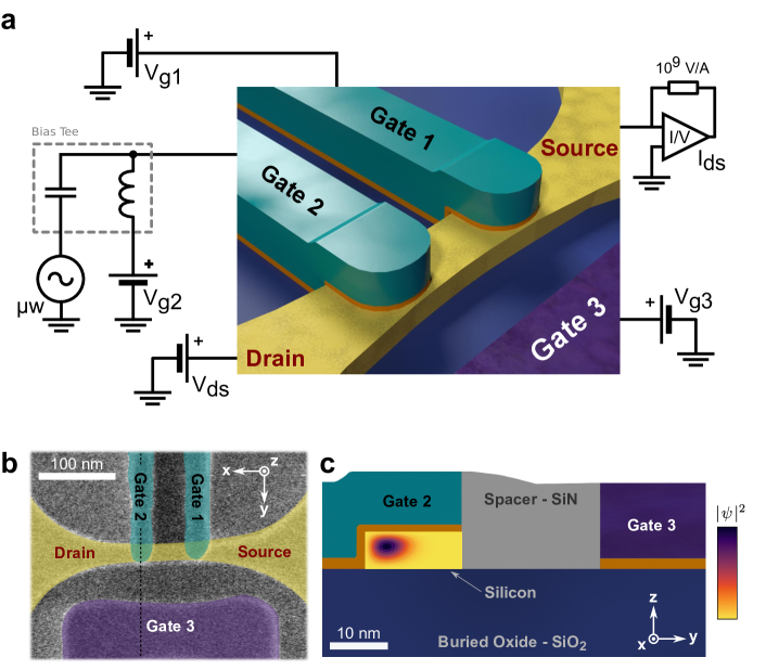
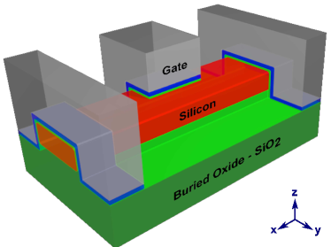
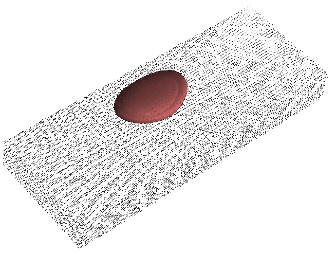
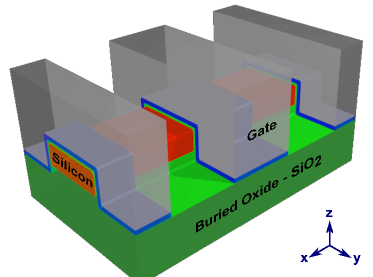
The experiment is carried out on a silicon nanowire device fabricated on a 300 mm diameter silicon-on-insulator wafer using an industrial-scale fabrication line Maurand16 . The device, shown in the schematic of fig. 1a and in the scanning electron micrograph of fig. 1b, consists of an undoped, nm-wide and nm-thick silicon channel oriented along , with -doped contacts. Two nm-wide top-gates (gate 1 and gate 2), spaced by nm, partially cover the channel. An additional gate (gate 3) is located on the opposite side at a distance of nm from the nanowire. Electron transport measurements were performed in a dilution refrigerator with a base temperature mK. At this temperature, two QDs in series, labeled as QD1 and QD2, can be defined by the accumulation voltages and applied to gate 1 and gate 2, respectively. The two QDs are confined against the nanowire edge covered by the gates, forming so-called “corner” dots Voisin14 ; Gonzalez15 , as confirmed by tight-binding simulations of the lowest energy states, whose wave-functions are shown in fig. 1c. We tune the electron filling of QD1 and QD2 down to relatively small occupation numbers and , respectively (, as inferred from the threshold voltage at room temperature and the charging energy Maurand16 ). The side gate is set to a negative V in order to further push the QD wave-functions against the opposite nanowire edges.
In the limit of vanishing inter-dot coupling and odd occupation numbers, both QD1 and QD2 have a spin-1/2 ground state. At finite magnetic field, , the respective spin degeneracies are lifted by the Zeeman energy , where is the Bohr magneton and is the Landé -factor, which is close to the bare electron value () for electrons in silicon Feher59b . In essence, our experiment consists in measuring electron transport through the double dot while driving EDSR in QD2. The polarized spin in QD1 acts as an effective “spin filter” regulating the current flow as a function of the spin admixture induced by EDSR in QD2. This Pauli blockade regime can be achieved only when the double dot is biased in a charge/spin configuration where inter-dot tunneling is forbidden by spin conservation Hanson07 . The simplest case involves the inter-dot charge transition , where one electron tunnels from QD1 into QD2. The two electrons may indeed form singlet (S) or triplet (T) states. While the singlet and triplet states are only weakly split by exchange interations and magnetic field and may both be loaded, the triplet states remain typically out of reach because they must involve some orbital excitation of QD2. The system may hence be trapped for long times in the states since tunneling from to the ground-state is forbidden by Pauli exclusion principle Hanson07 . This scenario can be generalized to the transitions where and are odd integers. The current is strongly suppressed unless EDSR mixes and by rotating the spin in QD2.
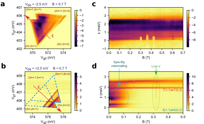
Because the opposite transition (or, more generically, ) is never blocked (there is always a (1,1) spin singlet to tunnel to), the Pauli blockade regime can be revealed by source-drain current rectification Ono02 . fig. 2 presents measurements of the source-drain current, , as a function of in a charge configuration exhibiting Pauli rectification. fig. 2a corresponds to a source-drain bias voltage mV and a magnetic field T. Current flows within characteristic triangular regions Hanson07 where the electrochemical potential of dot 1, , is lower than the electrochemical potential of dot 2, . The energy detuning between the two electrochemical potentials increases when moving along the red arrow. Current contains contributions from both elastic (i.e. resonant) and inelastic inter-dot tunneling. fig. 2b shows that reversing the bias voltage (i.e. mV) yields the desired Pauli rectification characterized by truncated current triangles (In Supplementary Note 1 we discuss the presence of a concomitant valley-blockade effect similar to the one shown by Hao et al. Hao14 ).
The extent of the spin-blockade region measured along the detuning axis corresponds to the energy splitting, , between singlet and triplet states in the charge configuration (which is equivalent to ), basically the singlet-triplet splitting in QD2 222in the case of non-degenerate triplet states at finite , is the splitting with respect to the triplet state, , with zero spin projection along . We find meV. figures 2-c) and 2-d) show as a function of and for negative and positive , respectively. As expected Ono02 , in the non-spin blocked polarity (fig. 2c) shows essentially no dependence on . In the opposite polarity, spin blockade is lifted at low field ( T), due to spin-flip cotunneling Lai11 ; Yamahata12 , as well as at T. This unexpected feature will be discussed later.
We now focus on the spin resonance experiment. To manipulate the spin electrically, we set and in the spin blocked region and apply a microwave excitation of frequency on gate 2. fig. 3a displays as a function of and at constant power at the microwave source (The power at the sample depends on and is estimated to be peak at 9.6 GHz). Several lines of increased current are visible in this plot, highlighting resonances along which Pauli spin blockade is lifted. They are labeled A, B, C and V. In the simplest case, spin resonance occurs when the microwave photon energy matches the Zeeman splitting between the two spin states of a doublet, i.e. when . We assign such a resonance to line A, because line A extrapolates to the origin (, ). Its slope gives , which is compatible with the -factor expected for electrons in silicon Feher59b . Also line C extrapolates to the origin but with approximately half the slope (i.e. ). We attribute this line to a second-harmonic driving process Scarlino15 .
We now focus on resonances B and V. The slope of line B is also compatible with the electron -factor (). However, line B crosses zero-frequency at T, corresponding exactly to the magnetic field at which the non-dispersive resonance V appears. Consequently, line B can be assigned to transitions between spin states associated with two distinct orbitals. When these spin states cross at , Pauli spin blockade is lifted independently of the microwave excitation leading to the non-dispersive resonance V (see Supplementary Note 1 for details on the lifting of spin blockade at ).
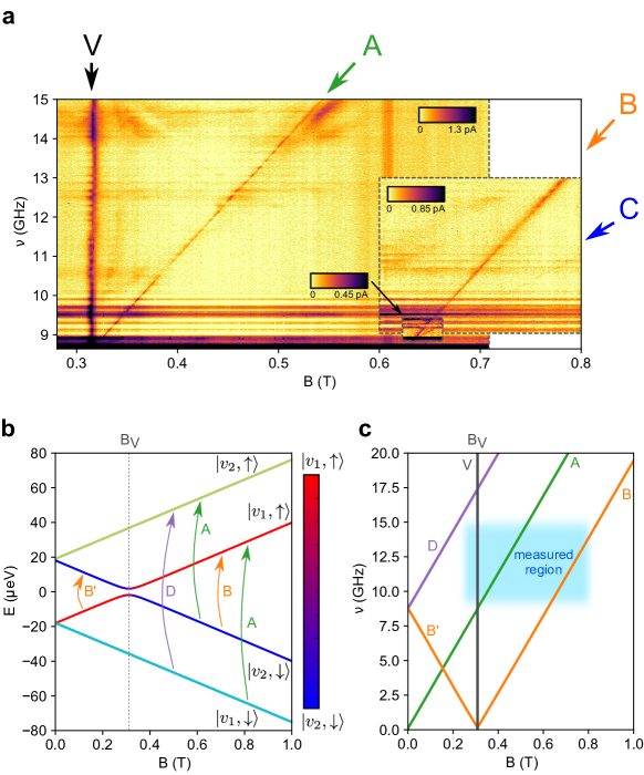
In order to understand the experimental EDSR spectrum of fig. 3a, we neglect in a first approximation the hybridization between the two QDs and consider only QD2 filled with one electron. We have developed a model that accounts for the mixing between spin and valley states due to SOC. In our silicon nanowire geometry, the confinement is strongest along the direction (normal to the SOI substrate), so that the low-energy levels belong to the valleys. Valley coupling at the Si/SiO2 interface lifts the twofold valley degeneracy Sham79 ; Saraiva09 ; Friesen10 ; Culcer10 ; Zwanenburg13 , resulting in two spin-degenerate valley eigenstates and with energies and , respectively, and a valley splitting . The expected energy diagram of the one-electron spin-valley states is plotted as a function of in fig. 3b (see Supplementary Note 2). The lowest spin-valley states can be identified as , anti-crossing at , and (the spin being quantized along ). From this energy diagram we assign the resonant transitions observed in fig. 3a as follows: line A corresponds to EDSR between states and (and between states and ); line B arises from EDSR between states and Scarlino17 ; line V is associated with the anti-crossing between states and when . We can thus measure eV. Note that the experimental EDSR spectrum does not capture all possible transitions since some of them fall out of the scanned range. fig. 3c shows the expected EDSR spectrum starting from and . The measured region is indicated in light blue (lower values of and could not be explored due to the onset of photon-assisted charge pumping and to the lifting of spin blockade, respectively).
The RF magnetic field associated with the microwave excitation on gate 2 is too weak to drive conventional ESR Golovach06 . Since a pure electric field cannot couple opposite spin states, SOC must be involved in the observed EDSR. The atomistic spin-orbit Hamiltonian primarily couples the different orbitals of silicon Chadi77 ; the states are, however, linear combinations of and orbitals with little admixture of and , which explains why the SOC matrix elements are weak in the conduction band of silicon. Yet the mixing between and by “inter-valley” SOC can be strongly enhanced when the splitting between these two states is small enough. We can capture the main physics and identify the relevant parameters using the simplest perturbation theory in the limit . The states and indeed read to first order in the spin-orbit Hamiltonian :
| (1a) | ||||
| (1b) | ||||
where:
| (2) |
Therefore, admixes a significant fraction of when the splitting between these two states decreases. As can be coupled to by the RF electric field, this allows for Rabi oscillations between and . Along line A, the Rabi frequency at resonance () reads:
| (3) |
where is the amplitude of the microwave modulation on gate 2, is the derivative of the total potential in the device with respect to the gate potential , and:
| (4) |
is the matrix element of between valleys and . The gate-induced electric field essentially drives motion in the plane. is small yet non negligible in SOI nanowire devices because the and wavefunctions show out of phase oscillations along , and can hence be coupled by the vertical electric field. The field along does not result in a sizable unless surface roughness disorder couples the motions along and in the plane Gamble13 ; Boross16 . Although is weak in silicon, SOC opens a path for an electrically driven spin resonance through a virtual transition from to , mediated by the microwave field, and then from to , mediated by SOC. Note, however, that the above equations are only valid at small magnetic fields where perturbation theory can be applied. A non-perturbative model valid at all fields is introduced in the Supplementary Note 2. It explicitly accounts for the anti-crossing (and strong hybridization by SOC) of states and near Yang13 ; Hao14 ; Huang2014 , but features the same matrix elements as above. This model shows that the Rabi frequency is maximal near , and confirms that there is a concurrent spin resonance , shifted by the valley splitting eV (lines B/B’ on fig. 3c), as well as, in principle, a possible resonance (line D).
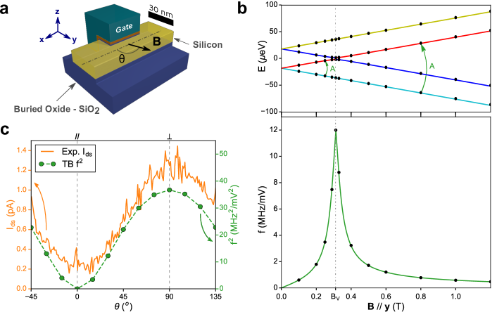
We have validated the above interpretation against tight-binding (TB) calculations. TB is well suited to that purpose as it accounts for valley and spin-orbit coupling at the atomistic level. We consider a simplified single-gate device model capturing the essential geometry (fig. 4a). A realistic surface roughness disorder with rms amplitude nm Bourdet16 is included in order to reduce the valley splitting down to the experimental value Culcer10 . A detailed description of the TB calculations is given in the Supplementary Note 3. The top panel of fig. 4b shows the dependence of the energy of the first four TB states . An anti-crossing is visible between states and at T. We calculate eV and V/V. The dependence of the TB Rabi frequency on line A is shown in the bottom panel of fig. 4b. There is a prominent peak near where and have a mixed / character. The maximum Rabi frequency is limited by while the full width at half maximum of the peak, T is controlled by the SOC matrix element (see Supplementary Note 3). The Rabi frequency remains however sizable over a few . We point out that and may depend on the actual roughness at the Si/SiO2 interface.
The calculated Rabi frequencies compare well against those reported for alternative silicon based systems. For example, the expected Rabi frequency is around 4.2 MHz for T, close to anticrossing field , and for a microwave excitation amplitude mV, close to the experimental value (see fig. 4b). This frequency is comparable with those achieved with coplanar antennas Pla2012 ; Veldhorst14 and in some experiments with micromagnets Kawakami14 ; Takeda16 .
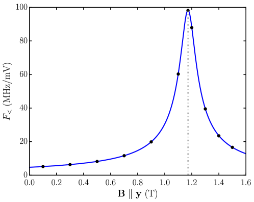
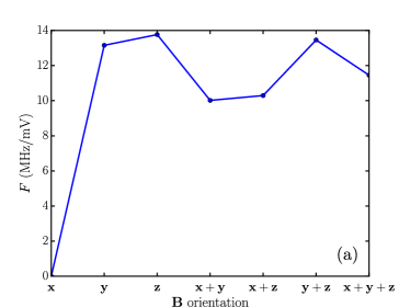
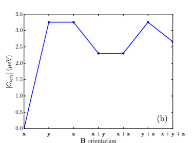
One of the most salient fingerprint of the above EDSR mechanism is the dependence of on the magnetic field orientation. Indeed, it must be realized that may vary with the orientation of the magnetic field (as the spin is quantized along in Eq. (2)). Actually, symmetry considerations supported by TB calculations show that and hence are almost zero when is aligned with the nanowire axis, due to the existence of a mirror plane perpendicular to that axis (see Supplementary Note 4). As a simple hint of this result, we may consider a generic Rashba SOC Hamiltonian of the form , where is the electric field, the momentum, and the Pauli matrices. Symmetric atoms on each side of the plane contribute to with opposite and components. Therefore, only the component of makes a non-zero contribution to , but does not couple opposite spins when . The current on line A is, to a first approximation, proportional to Koppens07 ; Schroer11 . The TB is plotted in fig. 4c as a function of the angle between an in-plane magnetic field and the nanowire axis . It shows the dependence expected from the above considerations. The experimental , also plotted in fig. 4c, shows the same behavior, supporting our interpretation. The fact that remains finite for may be explained by the fact that the symmetry plane is mildly broken by disorder and voltage biasing.
In a recent work, Huang et al. Huang17 proposed a mechanism for EDSR based on electrically induced oscillations of an electron across an atomic step at a Si/SiO2 or a Si/SiGe hetero-interface. The step enhances the SOC between the ground and the excited state of the same valley. The Rabi frequency is, however, limited by the maximal height of the step that the electron can overcome (typically 1 nm). The EDSR reported here has a different origin. It results from the finite SOC and dipole matrix elements between the ground-states of valleys and . These couplings are sizable only in a low-symmetry dot structure such as a corner QD Voisin14 , where there is only one mirror plane (see Supplementary Note 4). Indeed, we have verified that more symmetric device structures with at least two symmetry planes show a dramatic suppression of the SOC matrix element (since, as hinted above, each mirror rules out two out of three components in , leaving no possible coupling). This is the case of a typical nanowire field-effect transistor with the gate covering three sides of the nanowire channel, for which TB calculations give no EDSR since whatever the spin or magnetic field orientation. Conversely, the design of QDs without any symmetry left should maximize the opportunities for EDSR.
III Discussion
In conclusion, we have reported an experimental demonstration of electric-dipole, spin-valley resonance mediated by intrinsic SOC in a silicon electron double QD. Although SOC is weak in silicon, its effect can be enhanced in the corner QDs of an etched SOI device, owing to their reduced symmetry. SOC enables EDSR on the spin-split doublet of the first, lowest energy valley by mixing the up-spin state of that valley with the down-spin state of the second valley. The EDSR Rabi frequency is strongly enhanced near the corresponding anti-crossing, namely when the valley and Zeeman splittings are close enough. This enhancement comes with a price though, since we expect the spin relaxation time (and presumably also the spin coherence time ) to be simultaneously reduced Yang13 ; Huang2014 . Therefore, we anticipate that the efficiency of the reported EDSR mechanism for spin qubit manipulation will be conditioned by the possibility to tune the valley splitting , in order to bring the qubit near the anti-crossing point for manipulation, then away from the anti-crossing point to mitigate decoherence. Given the strong dependence of the valley splitting on gate voltages in silicon-based devices Goswami07 ; Takashina2006 , this possibility appears within reach and will be addressed in future experiments.
Methods
The silicon nanowire transistors are manufactured on a 300 mm Silicon-On-Insulator (SOI) processing line Maurand16 . first, silicon nanowires are etched from a SOI wafer with a 12 nm thick undoped silicon layer and a 145 nm thick buried oxide. The nanowire channels are oriented along the direction. The width of the nanowires, initially defined by deep ultra-violet (DUV) lithography, is trimmed down to about 30 nm by a well-controlled etching process. Two parallel top-gates, nm wide and spaced by nm are patterned with -beam lithography in order to control the double quantum dot. An additional side gate is also placed parallel to the nanowire at a distance of 50 nm in order to strengthen confinement in the corner dots of the Si nanowire. The gate stack consists in a 2.5 nm thick layer of SiO2, a 1.9 nm thick layer of HfO2, a thin ( nm) layer of TiN metal and a much thicker ( nm) layer of polysilicon. Then, insulating SiN spacers are deposited all around the gates and are etched. Their width is deliberately large ( nm) in order to cover completely the nanowire channel between the two gates and protect it from subsequent ion implantation. Arsenic and phosphorous are indeed implanted in order to achieve low resistance source/drain contacts. The wide spacers also limit dopant diffusion from the heavily implanted contact regions into the channel. The dopants are activated by spike annealing followed by silicidation. The devices are finalized with a standard microelectronics back-end of line process.
The devices are first screened at room temperature. Those showing the best performances (symmetrical characteristics for both top gates with no gate leakage current, low subthreshold swing) are cleaved from the original 300-mm wafer in order to be mounted on a printed-circuit-board chip carrier with high-frequency lines. The sample is measured in a wet dilution fridge with a base temperature mK. The magnetic field is applied by means of a 2D superconducting vector magnet in the plane parallel to the SOI wafer.
All terminals are connected with bonding wires to DC lines; gate 2 is also connected with a bias-tee to a microwave line. The DC block is a low rise-time Tektronik PSPL5501A, while the RF filter is made with a 10 k SMD resistance mounted on the chip carrier plus a wire acting as inductor. The DC voltages are generated at room temperature by custom battery-powered opto-isolated voltage sources. The microwave signal is generated by a commercial analog microwave generator (Anritsu MG3693C). The RF line is equipped with a series of attenuators at room temperature and in the cryostat for signal thermalization ( K), with a total attenuation of dB at 10 GHz. The current in the nanowire is measured by a custom transimpedance amplifier with a gain of V/A and then digitized by a commercial multimeter (Agilent 34410A).
Data availability
The data that support the findings of this study are available from the corresponding authors upon reasonable request.
Acknowledgements.
This work was supported by the European Union’s Horizon 2020 research and innovation program under grant agreement No 688539 MOSQUITO. Part of the calculations were run on the TGCC/Curie and CINECA/Marconi machines using allocations from GENCI and PRACE. We thank Cosimo Orban for the 3D rendering of the sample.Competing interests
The authors declare no competing financial interests.
Author contributions
H.B., R.L., L.H., S.B., and M.V. led device fabrication. A. Corna performed the experiment with help from R.M., A. Crippa and D.K.-P. under the supervision of X.J., S.D.F. and M.S. L. B. and Y.-M.N. did the modeling and simulations. M.V., X.J., S.D.F. and M.S led the all project. All authors co-wrote the manuscript.
Corresponding authors
Correspondence and requests of material should be addressed to Marc Sanquer
(marc.sanquer@cea.fr), Silvano De Franceschi (silvano.defranceschi@cea.fr) or Yann-Michel Niquet (yann-michel.niquet@cea.fr).
References
- (1) Zwanenburg, F. A. et al. Silicon quantum electronics. Review of Modern Physics 85, 961 (2013). URL https://dx.doi.org/10.1103/RevModPhys.85.961.
- (2) Tyryshkin, A. M. et al. Electron spin coherence exceeding seconds in high-purity silicon. Nature Materials 11, 143 (2012). URL https://dx.doi.org/10.1038/nmat3182.
- (3) Veldhorst, M. et al. An addressable quantum dot qubit with fault-tolerant control-fidelity. Nature Nanotechnology 9, 981 (2014). URL https://dx.doi.org/10.1038/nnano.2014.216.
- (4) Laucht, A. et al. Electrically controlling single-spin qubits in a continuous microwave field. Science Advances 1, e1500022 (2015). URL https://dx.doi.org/10.1126/sciadv.1500022.
- (5) Veldhorst, M. et al. A two-qubit logic gate in silicon. Nature 526, 410 (2015). URL https://dx.doi.org/10.1038/nature15263.
- (6) Pioro-Ladrière, M. et al. Electrically driven single-electron spin resonance in a slanting zeeman field. Nature Physics 4, 776 (2008). URL https://dx.doi.org/10.1038/nphys1053.
- (7) Kawakami, E. et al. Electrical control of a long-lived spin qubit in a Si/SiGe quantum dot. Nature Nanotechnology 9, 666 (2014). URL https://dx.doi.org/10.1038/nnano.2014.153.
- (8) Rančić, M. J. & Burkard, G. Electric dipole spin resonance in systems with a valley-dependent factor. Physical Review B 93, 205433 (2016). URL https://dx.doi.org/10.1103/PhysRevB.93.205433.
- (9) Takeda, K. et al. A fault-tolerant addressable spin qubit in a natural silicon quantum dot. Science Advances 2, e1600694 (2016). URL https://dx.doi.org/10.1126/sciadv.1600694.
- (10) Maurand, R. et al. A cmos silicon spin qubit. Nature Communications 7, 13575 (2016). URL https://dx.doi.org/10.1038/ncomms13575.
- (11) Nestoklon, M. O., Golub, L. E. & Ivchenko, E. L. Spin and valley-orbit splittings in heterostructures. Physical Review B 73, 235334 (2006). URL https://dx.doi.org/10.1103/PhysRevB.73.235334.
- (12) Hao, X., Ruskov, R., Xiao, M., Tahan, C. & Jiang, H. Electron spin resonance and spin-valley physics in a silicon double quantum dot. Nature Communications 5, 3860 (2014). URL https://dx.doi.org/10.1038/ncomms4860.
- (13) Schoenfield, J. S., Freeman, B. M. & Jiang, H. Coherent manipulation of valley states at multiple charge configurations of a silicon quantum dot device. Nature Communications 8, 64 (2017). URL https://dx.doi.org/10.1038/s41467-017-00073-x.
- (14) Jock, R. M. et al. Probing low noise at the MOS interface with a spin-orbit qubit. arXiv 1707.04357 (2017). URL https://arxiv.org/abs/1707.04357.
- (15) Veldhorst, M. et al. Spin-orbit coupling and operation of multivalley spin qubits. Physical Review B 92, 201401(R) (2015). URL https://dx.doi.org/10.1103/PhysRevB.92.201401.
- (16) Ruskov, R., Veldhorst, M., Dzurak, A. S. & Tahan, C. Electron g-factor of valley states in realistic silicon quantum dots. arXiv 1708.04555 (2017). URL https://arxiv.org/abs/1708.04555.
- (17) Sham, L. J. & Nakayama, M. Effective-mass approximation in the presence of an interface. Physical Review B 20, 734 (1979). URL https://dx.doi.org/10.1103/PhysRevB.20.734.
- (18) Saraiva, A. L., Calderon, M. J., Hu, X., Das Sarma, S. & Koiller, B. Physical mechanisms of interface-mediated intervalley coupling in si. Physical Review B 80, 081305(R) (2009). URL https://dx.doi.org/10.1103/PhysRevB.80.081305.
- (19) Friesen, M. & Coppersmith, S. N. Theory of valley-orbit coupling in a Si/SiGe quantum dot. Physical Review B 81, 115324 (2010). URL https://dx.doi.org/10.1103/PhysRevB.81.115324.
- (20) Culcer, D., Hu, X. & Das Sarma, S. Interface roughness, valley-orbit coupling, and valley manipulation in quantum dots. Physical Review B 82, 205315 (2010). URL https://dx.doi.org/10.1103/PhysRevB.82.205315.
- (21) Goswami, S. et al. Controllable valley splitting in silicon quantum devices. Nature Physics 3, 41 (2007). URL https://dx.doi.org/10.1038/nphys475.
- (22) Yang, C. H. et al. Spin-valley lifetimes in a silicon quantum dot with tunable valley splitting. Nature Communications 4, 2069 (2013). URL https://dx.doi.org/10.1038/ncomms3069.
- (23) Rashba, E. I. Theory of electric dipole spin resonance in quantum dots: Mean field theory with gaussian fluctuations and beyond. Physical Review B 78, 195302 (2008). URL https://dx.doi.org/10.1103/PhysRevB.78.195302.
- (24) Huang, P. & Hu, X. Spin relaxation in a si quantum dot due to spin-valley mixing. Physical Review B 90, 235315 (2014). URL https://dx.doi.org/10.1103/PhysRevB.90.235315.
- (25) Golovach, V. N., Borhani, M. & Loss, D. Electric-dipole-induced spin resonance in quantum dots. Physical Review B 74, 165319 (2006). URL https://dx.doi.org/10.1103/PhysRevB.74.165319.
- (26) Nowack, K. C., Koppens, F. H. L., Nazarov, Y. V. & Vandersypen, L. M. K. Coherent control of a single electron spin with electric fields. Science 318, 1430 (2007). URL https://dx.doi.org/10.1126/science.1148092.
- (27) Nadj-Perge, S., Frolov, S. M., Bakkers, E. P. A. M. & Kouwenhoven, L. P. Spin-orbit qubit in a semiconductor nanowire. Nature 468, 1084 (2010). URL https://dx.doi.org/10.1038/nature09682.
- (28) Pribiag, V. S. et al. Electrical control of single hole spins in nanowire quantum dots. Nature Nanotechnology 8, 170 (2013). URL https://dx.doi.org/10.1038/nnano.2013.5.
- (29) Voisin, B. et al. Few-electron edge-state quantum dots in a silicon nanowire field- effect transistor. Nano Letters 14, 2094 (2014). URL https://dx.doi.org/10.1021/nl500299h.
- (30) Gonzalez-Zalba, M. F., Barraud, S., Ferguson, A. J. & Betz, A. C. Probing the limits of gate-based charge sensing. Nature Communications 6, 6084 (2015). URL https://dx.doi.org/10.1038/ncomms7084.
- (31) Feher, G. Electron spin resonance experiments on donors in silicon. i. electronic structure of donors by the electron nuclear double resonance technique. Physical Review 114, 1219 (1959). URL https://dx.doi.org/10.1103/PhysRev.114.1219.
- (32) Hanson, R., Petta, J. R., Tarucha, S. & Vandersypen, L. M. K. Spins in few-electron quantum dots. Reviews of Modern Physics 79, 1217 (2007). URL https://dx.doi.org/10.1103/RevModPhys.79.1217.
- (33) Ono, K., Austing, D. G., Tokura, Y. & Tarucha, S. Current rectification by pauli exclusion in a weakly coupled double quantum dot system. Science 297, 1313 (2002). URL https://dx.doi.org/10.1126/science.1070958.
- (34) Lai, N. S. et al. Pauli spin blockade in a highly tunable silicon double quantum dot. Scientific Reports 1, 110 (2011). URL https://dx.doi.org/10.1038/srep00110.
- (35) Yamahata, G. et al. Magnetic field dependence of pauli spin blockade: A window into the sources of spin relaxation in silicon quantum dots. Physical Review B 86, 115322 (2012). URL https://dx.doi.org/10.1103/PhysRevB.86.115322.
- (36) Scarlino, P. et al. Second-harmonic coherent driving of a spin qubit in a Si / SiGe quantum dot. Physical Review Letters 115, 106802 (2015). URL https://dx.doi.org/10.1103/PhysRevLett.115.106802.
- (37) Scarlino, P. et al. Dressed photon-orbital states in a quantum dot: Intervalley spin resonance. Physical Review B 95, 165429 (2017). URL https://dx.doi.org/10.1103/PhysRevB.95.165429.
- (38) Chadi, D. J. Spin-orbit splitting in crystalline and compositionally disordered semiconductors. Physical Review B 16, 790 (1977). URL https://dx.doi.org/10.1103/PhysRevB.16.790.
- (39) Gamble, J. K., Eriksson, M. A., Coppersmith, S. N. & Friesen, M. Disorder-induced valley-orbit hybrid states in Si quantum dots. Physical Review B 88, 035310 (2013). URL https://dx.doi.org/10.1103/PhysRevB.88.035310.
- (40) Boross, P., Széchenyi, G., Culcer, D. & Pályi, A. Control of valley dynamics in silicon quantum dots in the presence of an interface step. Physical Review B 94, 035438 (2016). URL https://dx.doi.org/10.1103/PhysRevB.94.035438.
- (41) Bourdet, L. et al. Contact resistances in trigate and finfet devices in a non-equilibrium green’s functions approach. Journal of Applied Physics 119, 084503 (2016). URL https://dx.doi.org/10.1063/1.4942217.
- (42) Pla, J. J. et al. A single-atom electron spin qubit in silicon. Nature 489, 541 (2012). URL https://dx.doi.org/10.1038/nature11449.
- (43) Koppens, F. H. L. et al. Detection of single electron spin resonance in a double quantum dot. Journal of Applied Physics 101, 081706 (2007). URL https://dx.doi.org/10.1063/1.2722734.
- (44) Schroer, M. D., Petersson, K. D., Jung, M. & Petta, J. R. Field tuning the g factor in InAs nanowire double quantum dots. Physical Review Letters 107, 176811 (2011). URL https://dx.doi.org/10.1103/PhysRevLett.107.176811.
- (45) Huang, W., Veldhorst, M., Zimmerman, N. M., Dzurak, A. S. & Culcer, D. Electrically driven spin qubit based on valley mixing. Physical Review B 95, 075403 (2017). URL https://dx.doi.org/10.1103/PhysRevB.95.075403.
- (46) Takashina, K., Ono, Y., Fujiwara, A., Takahashi, Y. & Hirayama, Y. Valley polarization in Si(100) at zero magnetic field. Physical Review Letters 96, 236801 (2006). URL https://dx.doi.org/10.1103/PhysRevLett.96.236801.
- (47) Niquet, Y. M., Rideau, D., Tavernier, C., Jaouen, H. & Blase, X. Onsite matrix elements of the tight-binding hamiltonian of a strained crystal: Application to silicon, germanium, and their alloys. Physical Review B 79, 245201 (2009). URL https://dx.doi.org/10.1103/PhysRevB.79.245201.
Supplementary notes for “Electrically driven electron spin resonance mediated by spin-valley-orbit coupling in a silicon quantum dot”
Supplementary note 1: Valleys and spin-valley blockade
In the main text, we have discussed the nature of the A, B, C and V line in a one-particle picture. In this supplementary note, we introduce a two-particle picture for the blockade, which accounts for the valley degree of freedom and gives a better description of the V line.
Spin blockade can arise when the current flows through the sequence of charge configurations , where and are the number of electrons in dots 1 and 2.Ono et al. (2002); Hanson et al. (2007) Indeed, the states can be mapped onto singlet and triplet states, while the states can be mapped onto singlet and triplet states. While the and states are almost degenerate, the and states can be significantly split because the state must involve some orbital excitation. The electron may enter in dot 1 through any of the configurations at high enough source-drain bias. Once in a state, the system may, however, get trapped for a long time if the states are still out of the bias window, because tunneling from to requires a spin flip. The current is hence suppressed. At reverse source-drain bias, the current flows through the sequence of charge configurations , which can not be spin-blocked, giving rise to current rectification (see Fig. 2 of main text).
The observation of inter-valleys resonances suggests that is even (otherwise only transitions between states would be observed in dot 2). We assume from now on that is also even. As a matter of fact, the absence of visible bias triangles for lower gate voltages suggests that , though we can not exclude the existence of extra triangles with currents below the detection limit.
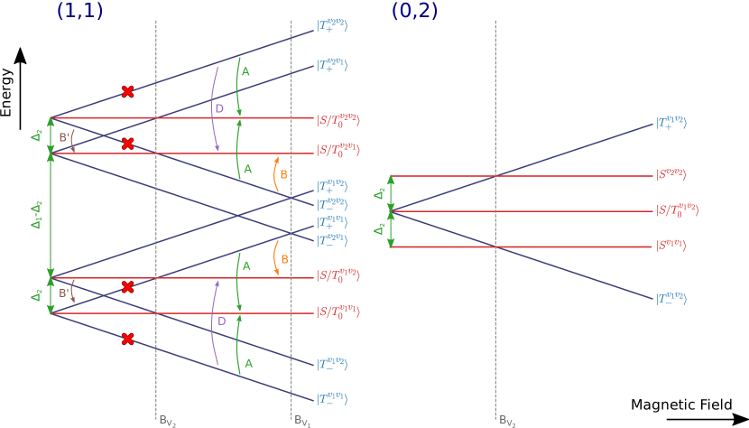
We discuss below the role of valley blockade in the present experiments. We assume the valley splitting is much larger in dot 1 () than in dot 2 (eV) due to disorder and bias conditions. The valley splitting in dot 1 is actually beyond the bandwidth of the EDSR setup. This reflects the stochastic variations from one dot to an other, as confirmed by tight-binding simulations.
In the charge configuration, the low-energy states can be characterized by their spin component [singlet (S) or triplet (T0, T-, T+)] and by the valley occupied in each dot ( or ). Sixteen states can be constructed in this way (see Fig. S1). We neglect in a first approximation the small exchange splitting between singlet and triplet states with same valley indices. The magnetic field splits the T- (total spin ) and T+ states () from the S and states (). The splitting between T+ and T- is .
Similar states can be constructed in the charge configuration. The and are detuned by the bias on gates 1 and 2. We focus on detunings smaller than the orbital singlet-triplet splitting meV, so that neither the nor the triplets can be reached from the states.
Given the small eV extracted from spin resonance, we need, however, to reconsider the mechanisms for current rectification. Indeed, the system must be spin-and-valley blockedHao et al. (2014) since the detuning is typically much larger than so that states are accessible in the bias window. Assuming that both spin and valley are conserved during tunneling, the spin and valley blocked states are actually , , and . Although and are, in principle, also spin and valley blocked, they may be mixed with the nearly degenerate and states by, e.g., spin-orbit coupling (SOC) and nuclear spin disorder,Koppens et al. (2005); Nadj-Perge et al. (2010) and be therefore practically unblocked.
We can now refine the interpretation of the different lines. Each one corresponds to a different set of transitions between blocked and unblocked states. Line A corresponds to transitions between and / states, and to transitions between and / states. Line B corresponds to transitions between and / states, and between and / states. The line D on Fig. 3 of the main text would correspond to transitions between and / states, and between and / states. These transitions give rise to the same spectrum as in the one-particle picture.
Line V is independent on the microwave frequency and also appears when no microwaves are applied. At the magnetic field , the states and , as well as the states and are almost degenerate. The mixing of these near degenerate blocked and unblocked states by SOC lifts spin and valley blockade of the and states, giving rise to an excess of current at independent on the microwave excitation.
Note that we also expect a horizontal line H (independent on the magnetic field) corresponding to transitions between and , and between and , at frequency GHz. Horizonal lines are indeed visible in the expected frequency range on Fig. 3a (main text), but they can not be unequivocally assigned due to the onset of photon-assisted charge pumping resulting in parasitic features.
Supplementary note 2: Theory
In this supplementary note, we propose a model for spin-orbit driven EDSR in silicon quantum dots accounting for the strong hybridization of the spin and valley states near the anti-crossing field .
We consider a silicon QD with strongest confinement along the direction so that the low-lying conduction band levels belong to the valleys. This dot is controlled by a gate with potential . In the absence of valley and spin-orbit coupling, the ground-state is fourfold degenerate (twice for spins and twice for valleys). Valley couplingSham and Nakayama (1979); Saraiva et al. (2009); Friesen and Coppersmith (2010); Culcer et al. (2010); Zwanenburg et al. (2013) splits this fourfold degenerate level into two spin-degenerate states and with energies and , separated by the valley splitting energy ( is the spin index). In the simplest approximation, and are bonding and anti-bonding combinations of the states.
The remaining spin degeneracy can be lifted by a static magnetic field . The energy of state is then ( for up states, for down states, the spin being quantized along ). Here is the gyro-magnetic factor of the electrons, which is expected to be close to in silicon.Feher (1959) We may neglect the effects of the magnetic field on the orbital motion of the electrons in a first approximation. The wave functions can then be chosen real.
The gate potential is modulated by a RF signal with frequency and amplitude in order to drive EDSR between states and . At resonance , the Rabi frequency reads:
| (S1) |
where is the derivative of the total potential in the device with respect to .333If the electrostatics of the device is linear, , where is the total potential in the empty device with the gate at potential , and all other terminals grounded. We discard the effects of the displacement currents (concomitant ESR), which are negligible.Golovach et al. (2006) In the absence of SOC, is zero as an electric field can not couple opposite spins.
As discussed in the main text, spin-orbit couples the orbital and spin motions of the electron.Nestoklon et al. (2006); Yang et al. (2013); Huang and Hu (2014); Hao et al. (2014); Veldhorst et al. (2015); Huang et al. (2017) “Intra-valley” SOC mixes spins within the or the valley, while “inter-valley” SOC mixes spins between the and valleys. Both intra-valley and inter-valley SOC may couple with the excited states of valley 1. Inter-valley SOC may also couple with all states. Its effects can be strongly enhanced if the valley splitting is small enough. Indeed, in the simplest non-degenerate perturbation theory, the states and read to first order in the spin-orbit Hamiltonian :
| (S2a) | ||||
| (S2b) | ||||
with
| (S3a) | ||||
| (S3b) | ||||
The above equalities follow from time-reversal symmetry considerations for real wave functions. is complex and is real. We have neglected all mixing beyond the four , because the higher-lying excited states usually lie meV above and (as inferred from on Fig. 2, main text).
Inserting Eqs. (S2) into Eq. (S1), then expanding in powers of yields to first order in and :
| (S4) |
where
| (S5) |
is the electric dipole matrix element between valleys and . As expected, the Rabi frequency is proportional to , , and to (as the contributions from the terms in Eqs. (S2) cancel out if time-reversal symmetry is not broken by the terms of the denominators). It is also inversely proportional to ; namely the smaller the valley splitting, the faster the rotation of the spin. does not contribute to lowest order because it couples states with the same spin.
and are known to be small in the conduction band of silicon.Nestoklon et al. (2006); Yang et al. (2013); Hao et al. (2014); Veldhorst et al. (2015); Huang et al. (2017) Actually, is zero in any approximation that completely decouples the valleys (such as the simplest effective mass approximation). It is, however, finite in tight-bindingDi Carlo (2003); Delerue and Lannoo (2004) or advanced modelsSaraiva et al. (2009); Culcer et al. (2010) for the conduction band of silicon. According to Eq. (S4), the Rabi frequency can be significant if is close enough to to enhance spin-valley mixing by . This happens when is small and/or when (see later discussion). The main path for EDSR is then the virtual transition from to (mediated by ), then from to (mediated by the RF field).
The above equations are valid only for very small magnetic fields , as non-degenerate perturbation theory breaks down near the anti-crossing between and when (see Fig. 3b of the main text). We may deal with this anti-crossing using degenerate perturbation theory in the subspace, while still using Eq. (S2a) for state . However, such a strategy would spoil the cancellations between and needed to achieve the proper behavior when . We must, therefore, treat SOC in the full subspace.Yang et al. (2013); Huang and Hu (2014)
The total Hamiltonian then reads:
| (S6) |
As discussed before, is not expected to make significant contributions to the EDSR as it mixes states with the same spin. We may therefore set for practical purposes; then splits into two blocks in the and subspaces. The diagonalization of the block yields energies:
| (S7) |
and eigenstates:
| (S8a) | ||||
| (S8b) | ||||
with:
| (S9a) | ||||
| (S9b) | ||||
and:
| (S10) |
Likewise, the diagonalization of the block yields energies:
| (S11) |
and eigenstates:
| (S12a) | ||||
| (S12b) | ||||
with:
| (S13a) | ||||
| (S13b) | ||||
and:
| (S14) |
We can finally compute the Rabi frequencies for the resonant transitions between the ground-state and the mixed spin and valley states :
| (S15a) | ||||
| (S15b) | ||||
The Rabi frequencies for the resonant transitions between and are equivalent. We can also compute the Rabi frequency between the states :
| (S16) |
as well as the Rabi frequency between the states :
| (S17) |
where and . The expansion of Eq. (S15a) in powers of and yields back Eq. (S4) at low magnetic fields. Yet Eqs. (S15) are valid up to much larger magnetic field (typically , where is the energy of the next-lying state).
The typical energy diagram is plotted as a function of in Fig. 3b of the main text. From an experimental point of view, line A of Fig. 3b corresponds to () or (), while line B corresponds to . The line D on Fig. 3c would correspond to .
Supplementary note 3: Tight-binding modeling
III.1 Methodology and devices
We have validated the model of supplementary note 2 against tight-binding (TB) calculations.Di Carlo (2003); Delerue and Lannoo (2004) TB is well suited to the description of such devices as it accounts for valley and spin-orbit coupling at the atomistic level (without the need for, e.g., extrinsic Rashba or Dresselhaus-like terms in the Hamiltonian).
We consider the prototypical device of Fig. S2a. The silicon nanowire (dielectric constant ) is nm wide and nm thick. It is etched in a SOI film on top a 25 nm thick buried oxide (BOX).444The BOX used in the simulations is thinner than in the experiments (145 nm) for computational convenience. We have checked that this does not have any sizable influence on the results. The QD is defined by the central, 30 nm long gate. This gate covers only part of the nanowire in order to confine a well-defined “corner state”. The QD is surrounded by two lateral gates that control the barrier height between the dots (periodic boundary conditions being applied along the wire). The front gate stack is made of a layer of SiO2 () and a layer of HfO2 (). The device is embedded in Si3N4 (). We did not include the lateral gate in the simulations. All terminals are grounded except the central gate.
We compute the first four eigenstates of this device using a TB model.Niquet et al. (2009) The dangling bonds at the surface of silicon are saturated with pseudo-hydrogen atoms. We include the effects of SOC and magnetic field. The SOC Hamiltonian is written as a sum of intra-atomic termsChadi (1977)
| (S18) |
where is the angular momentum on atom , is the spin and is the SOC constant of silicon. The action of the magnetic field on the spin is described by the bare Zeeman Hamiltonian , and the action of the magnetic field on the orbital motion of the electrons is accounted for by Peierl’s substitution.Graf and Vogl (1995) We can then monitor the different Rabi frequencies
| (S19) |
The wave function of the ground-state is plotted in Fig. S2b ( V). It is, as expected for etched SOI structures, confined in a “corner dot” below the gate. Note that this TB description goes beyond the model of supplementary note 2 in including the action of the magnetic field on the orbital motion, and in dealing with all effects non-perturbatively.
In the following, we define (nanowire axis), (perpendicular to the nanowire) and (perpendicular to the substrate).
III.2 Dependence on the magnetic field amplitude
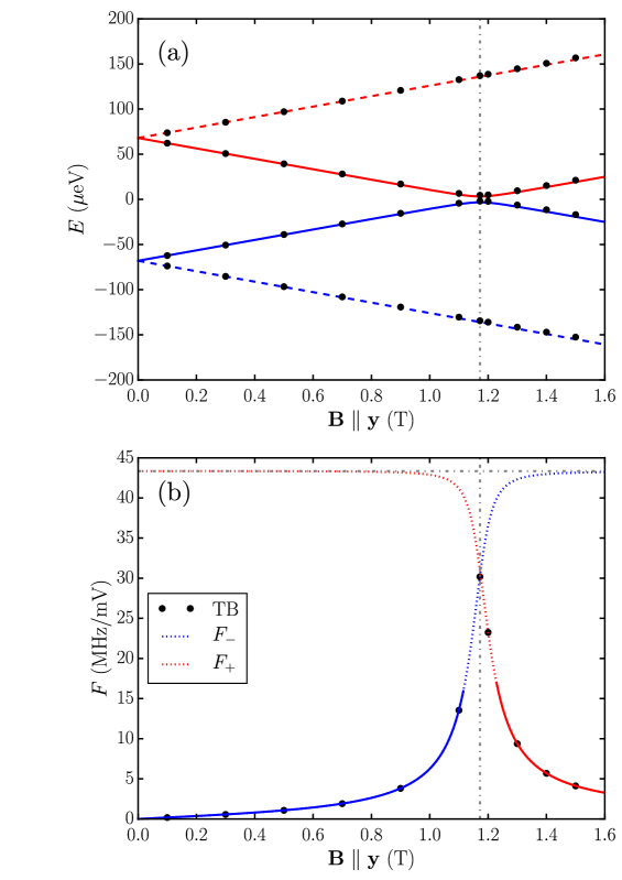
The energy of the first four eigenstates is plotted as a function of in Fig. S3a. States … all belong to the valleys, as confinement remains stronger along than along in a very wide range of gate voltages. The lowest eigenstate can be identified with , the second one and the third one with (/ anti-crossing at T), and the fourth one with .
The reduced TB Rabi frequency between and is plotted as a function of in Fig. S3. Hence before the anti-crossing between and at , and after that anti-crossing. This transition corresponds to line A of the main text. The dependence of on is strongly non-linear, with a prominent peak near the anti-crossing.
We can then switch off SOC, recompute the TB eigenstates at , extract
| (S20a) | ||||
| (S20b) | ||||
| (S20c) | ||||
| (S20d) | ||||
and input these into Eqs. (S15). As shown in Fig. S3, Eqs. (S15) perfectly reproduce the TB data. There are, in particular, no virtual transitions outside the lowest four that contribute significantly to the Rabi frequency.
The reduced TB Rabi frequency is also plotted on Fig. S4. This transition corresponds to line B of the main text. It also shows a peak near the , and is pretty strong.
In the present device, the TB valley splitting is much larger than the experiment (eV). However, decreases once surface roughness is introducedCulcer et al. (2010) and can range from a few tens to a few hundreds of eV depending on the bias conditions. The TB data reported in Fig. 4 of the main text have been computed for a particular realization of surface roughness disorder that reproduces the experimental eV. The surface roughness profiles used in these simulations have been generated from a Gaussian auto-correlation function with rms nm and correlation length nm.Goodnick et al. (1985); Bourdet et al. (2016) Note that disorder also reduces , , and . A strategy for the control of the valley splitting in etched SOI devices will be reported elsewhere.
It is clear from Eqs. (S15) that , where is limited only by the dipole matrix element . In particular, near the anti-crossing field ,
| (S21) |
only depends on . The SOC matrix element actually controls the width of the peak around . The full width at half-maximum of this peak () indeed reads:
| (S22) |
Supplementary note 4: Role of symmetries
To highlight the role of symmetries, we plot the reduced TB Rabi frequency (corresponding to line A of the main text) and SOC matrix element as a function of the orientation of the magnetic field in Fig. S5 (same bias conditions as in Fig. S3, T). As expected, shows the same trends as – although there are small discrepancies. These discrepancies result from the effects of the magnetic field on the orbital motion of the electron, dismissed in the supplementary note 2.
Strikingly, the SOC matrix element and Rabi frequency are almost zero when the magnetic field is aligned with the nanowire axis (). The dependence of on the magnetic field (or spin) orientation suggests that only the term of the SOC Hamiltonian is relevant for this matrix element. This can be supported by a symmetry analysis. Now quantifying the spin along , the TB SOC Hamiltonian [Eq. (S18)] reads:
| (S23) |
where are the Pauli matrices, and is the component of the angular momentum on atom . The device of Fig. S6 is only invariant by reflection through the plane (space group ). The table of characters of this space group is reproduced in Table 1. Let us remind that for any observable , unitary transform (symmetry operation) , and wave functions and ,
| (S24) |
Both and states belong to the irreducible representation of . Therefore, and . Also, is compatible with the symmetry, so that . Therefore, Eq. (S24) does not set any condition on . However, transforms a orbital into a orbital, hence transforms into , into , but leaves invariant (see Table 2). Eq. (S24) then imposes that and can not couple the and states. This is why only the term of the atomistic SOC Hamiltonian makes a non-zero contribution. As a result, and the Rabi frequency are proportional to , where is the angle between and an in-plane magnetic field. The effective SOC Hamiltonian between and is likely dominated by Rashba-type contributions of the form (where and are the momenta along and ). These Rashba-type contributions may arise from the electric field of the gate along and , and/or from the top and lateral Si/SiO2 interfaces bounding the corner dot.
How far is the EDSR connected with the formation of corner dots in etched SOI structures ? To answer this question, we have computed the Rabi frequency in a standard “Trigate” device where the gate surrounds the channel on three sides (see Fig. S6a). The dimensions are the same as in Fig. S2, but the central gate now covers the totality of the nanowire. As shown in Fig. S6b, the low-lying conduction band states are still confined at the top interface, but the wave function is symmetric with respect to the plane (no “corner” effect at zero back gate voltage). It turns out that there is no EDSR whatever the orientation of the magnetic field. Actually, the SOC matrix element is zero for all spin orientations.
Therefore the confinement in a corner dot seems to be a pre-requisite for a sizable EDSR. As a matter of fact, the devices of Figs. S6 and S2 have different symmetries. Indeed, the device of Fig. S6 is invariant by reflections through the and planes, and by the twofold rotation around the axis (space group ). The states and of this device again belong to the irreducible representation of (Table 1). For the same reasons as before, Eq. (S24) does not set any condition on . The existence of a mirror still imposes that only can couple and states. Yet the introduction of a mirror, which leaves only invariant, prevents such a coupling. Therefore, none of the operators , and can couple the and states. is thus zero, and SOC-mediated EDSR is not possible.
To conclude, the symmetry must be sufficiently low in order to achieve EDSR in the conduction band of silicon. This condition is realized in corner dots where there is only one mirror left (yet preventing EDSR for a magnetic field along the wire axis). The design of geometries without any symmetry left would in principle maximize the opportunities for EDSR.
References
- Ono et al. (2002) K. Ono, D. G. Austing, Y. Tokura, and S. Tarucha, Science 297, 1313 (2002).
- Hanson et al. (2007) R. Hanson, J. R. Petta, S. Tarucha, and L. M. K. Vandersypen, Reviews of Modern Physics 79, 1217 (2007).
- Hao et al. (2014) X. Hao, R. Ruskov, M. Xiao, C. Tahan, and H. Jiang, Nature Communications 5, 3860 (2014).
- Koppens et al. (2005) F. H. L. Koppens, J. A. Folk, J. M. Elzerman, R. Hanson, L. H. W. van Beveren, I. T. Vink, H. P. Tranitz, W. Wegscheider, L. P. Kouwenhoven, and L. M. K. Vandersypen, Science 309, 1346 (2005).
- Nadj-Perge et al. (2010) S. Nadj-Perge, S. M. Frolov, J. W. W. van Tilburg, J. Danon, Y. V. Nazarov, R. Algra, E. P. A. M. Bakkers, and L. P. Kouwenhoven, Physical Review B 81, 201305(R) (2010).
- Sham and Nakayama (1979) L. J. Sham and M. Nakayama, Physical Review B 20, 734 (1979).
- Saraiva et al. (2009) A. L. Saraiva, M. J. Calderon, X. Hu, S. Das Sarma, and B. Koiller, Physical Review B 80, 081305(R) (2009).
- Friesen and Coppersmith (2010) M. Friesen and S. N. Coppersmith, Physical Review B 81, 115324 (2010).
- Culcer et al. (2010) D. Culcer, X. Hu, and S. Das Sarma, Physical Review B 82, 205315 (2010).
- Zwanenburg et al. (2013) F. A. Zwanenburg, A. S. Dzurak, A. Morello, M. Y. Simmons, L. C. L. Hollenberg, G. Klimeck, S. Rogge, S. N. Coppersmith, and M. A. Eriksson, Review of Modern Physics 85, 961 (2013).
- Feher (1959) G. Feher, Physical Review 114, 1219 (1959).
- Golovach et al. (2006) V. N. Golovach, M. Borhani, and D. Loss, Physical Review B 74, 165319 (2006).
- Nestoklon et al. (2006) M. O. Nestoklon, L. E. Golub, and E. L. Ivchenko, Physical Review B 73, 235334 (2006).
- Yang et al. (2013) C. H. Yang, A. Rossi, R. Ruskov, N. S. Lai, F. A. Mohiyaddin, S. Lee, C. Tahan, G. Klimeck, A. Morello, and A. S. Dzurak, Nature Communications 4, 2069 (2013).
- Huang and Hu (2014) P. Huang and X. Hu, Physical Review B 90, 235315 (2014).
- Veldhorst et al. (2015) M. Veldhorst, R. Ruskov, C. H. Yang, J. C. C. Hwang, F. E. Hudson, M. E. Flatté, C. Tahan, K. M. Itoh, A. Morello, and A. S. Dzurak, Physical Review B 92, 201401(R) (2015).
- Huang et al. (2017) W. Huang, M. Veldhorst, N. M. Zimmerman, A. S. Dzurak, and D. Culcer, Physical Review B 95, 075403 (2017).
- Di Carlo (2003) A. Di Carlo, Semiconductor Science and Technology 18, R1 (2003).
- Delerue and Lannoo (2004) C. Delerue and M. Lannoo, Nanostructures: Theory and Modelling (Springer, New-York, 2004).
- Niquet et al. (2009) Y. M. Niquet, D. Rideau, C. Tavernier, H. Jaouen, and X. Blase, Physical Review B 79, 245201 (2009).
- Chadi (1977) D. J. Chadi, Physical Review B 16, 790 (1977).
- Graf and Vogl (1995) M. Graf and P. Vogl, Physical Review B 51, 4940 (1995).
- Goodnick et al. (1985) S. M. Goodnick, D. K. Ferry, C. W. Wilmsen, Z. Liliental, D. Fathy, and O. L. Krivanek, Physical Review B 32, 8171 (1985).
- Bourdet et al. (2016) L. Bourdet, J. Li, J. Pelloux-Prayer, F. Triozon, M. Cassé, S. Barraud, S. Martinie, D. Rideau, and Y.-M. Niquet, Journal of Applied Physics 119, 084503 (2016).