Field effect induced mesoscopic devices in depleted two dimensional electron systems
Abstract
Nanoelectronic devices embedded in the two-dimensional electron system (2DES) of a GaAs/AlGaAs heterostructure enable a large variety of applications from fundamental research to high speed transistors. Electrical circuits are thereby commonly defined by creating barriers for carriers by selective depletion of a pre-existing 2DES. Here we explore an alternative approach: we deplete the 2DES globally by applying a negative voltage to a global top gate and screen the electric field of the top gate only locally using nanoscale gates placed on the wafer surface between the plane of the 2DES and the top gate. Free carriers are located beneath the screen gates and their properties can be controlled by means of geometry and applied voltages. This method promises considerable advantages for the definition of complex circuits by the electric field effect as it allows to reduce the number of gates and simplify gate geometries. Examples are carrier systems with ring topology or large arrays of quantum dots. Here, we present a first exploration of this method pursuing field effect, Hall effect and Aharonov-Bohm measurements to study electrostatic, dynamic and coherent properties.
I introduction
The electric field effect is a powerful tool for nanoelectronics. It is widely used for creating potential barriers in a two-dimensional electron system (2DES) by applying voltages to individual metal gates placed on the wafer surface. When used with multiple individual gates it provides full tunability while being compatible with high mobility wafers. Alternative methods for structuring a 2DES include etching Behringer et al. (1987); Lee et al. (1989); Ford et al. (1990); Moon et al. (1998) and surface oxidation techniques Held et al. (1998); Heinzel et al. (2001). While they ensure additional possibilities in combination with in-plane side gates Wieck and Ploog (1990) or metal gates Held et al. (1999); Platonov et al. (2015), etching and oxidation techniques alone lack tunability. More importantly, they are restricted to wafers with a shallow 2DES causing a close proximity of surface states and doping atoms limiting the carrier mobility Walukiewicz et al. (1984) and the electrostatic stability at the nanoscale (related with the spectrum of charge noise Jung et al. (2004); Buizert et al. (2008); Taubert et al. (2008)). Applications based on the quantum mechanical coherence of localized carriers require superior control and stability favoring the field effect.
A straightforward and the most common approach to shape potential landscapes by the field effect, starting from an extended 2DES, is based on the controlled local depletion of the 2DES beneath individual surface gates. This approach works perfectly for relatively small structures with simple topology such as few coupled quantum dots Schröer et al. (2007); Forster et al. (2015) or quantum point contacts. However, an individually tunable one-dimensional array of quantum dots requires at least metal gates, while even more gates are needed for a two-dimensional array or for increased tunability. Failure of a single gate would alter the current path and typically make the entire device useless. Furthermore, non-trivial topologies such as an Aharonov-Bohm ring, allowing carriers to move in a circle around a depleted center, require voltage biasing of a center gate without depleting the surrounding carriers. This has been achieved by implementation of three-dimensional air bridges Buks et al. (1998); Chang et al. (2008). However, the fabrication of air bridges is rather complex and limited to relatively big structures.
In this article we propose an alternative method to define complex nanoelectronic circuits based on the field effect, offering full tunability of high quality devices. Compared to common strategies our method simplifies the production of ring topologies and offers the prospect of scalability while limiting the danger of general failure. Our idea, sketched in Fig. 1(a),
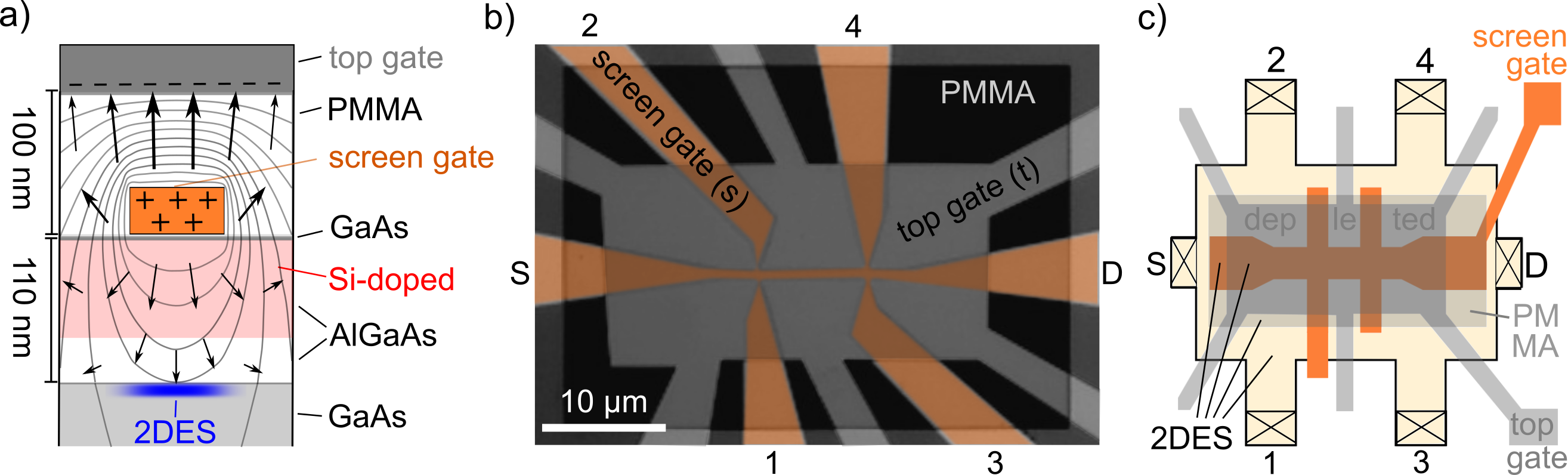
is based on globally depleting the 2DES using a single top gate while we place nanoscale screen gates between the top gate and the 2DES to locally shield the effect of the top gate and thereby regain free carriers. We electrically isolate the top gate from the screen gates using an about nm thick layer of cross-linked PMMA Zailer et al. (1996); Teh and Smith (2003), while the 2DES at the interface between AlGaAs and GaAs is separate from the screen gates on the wafer surface by another 110 nm consisting of the following electrically insulating layers: a 5 nm thick capping layer of GaAs to prevent oxidation of the surface, followed by 70 nm of homogeneously Si-doped Al0.36Ga0.64As, and 35 nm of undoped Al0.36Ga0.64As Note (1); Wieck and Reuter (2000)00footnotetext: Below this, there is a nm thick GaAs layer on top of periods of a superlattice of nm Al and nm As to stick segregating impurities during the MBE-growth at its interfaces and, thus, to keep the layers above clean. The 2DES is formed in the GaAs-layer close to the interface of the Al0.36Ga0.64As layer.. Carrier density and the detailed geometry of the confinement potential depend on the electric field at the 2DES and can be fine tuned by adjusting the voltages applied to both, the top gate and the screen gate. In Fig. 1(a) we sketch the screening effect on a grounded 2DES for the example of a positively charged screen gate beneath a negatively charged top gate. A global top gate above gates at the surface had been used before for different purposes . In a previous attempt to structure a 2DES, a single top gate was combined with a local dielectric to partially screen the field of the global top gate Ford et al. (1988, 1989). Here, the missing screen gate results in a reduced tunability compared to our approach. A global top gate has also been employed to decrease telegraph noise Buizert et al. (2008) or to incorporate carriers in undoped quantum wells Harrell et al. (1999); Chen et al. (2012). In the last two examples gates on the GaAs surface are used to locally deplete the 2DES while in our case carriers accumulate beneath the screen gate.
In Fig. 1(b) we display a scanning electron microscope (SEM) image of an actual Hall-bar sample and in Fig. 1(c) a descriptive sketch. The screen gate (s) directly on the sample surface is shown in orange, the top gate (t) above, which is electrically isolated by cross-linked PMMA, in light gray. By charging the top gate negatively in respect to the grounded 2DES and a grounded backgate at the bottom of the m thick wafer we deplete the 2DES beneath the top gate whereever it is not shielded by the screen gate. Below the top gate the shape of the screen gate corresponds to the approximate shape of the 2DES beneath. The screen gate in Fig. 1(b) defines a Hall-bar with source (S) and drain (D) for current and four side contacts used as voltage probes (1,2,3,4). The top gate includes a large center square and six arms reaching to the outside. The arms have the function to avoid electrical shorts between the six contacts outside of the Hall bar region where they would otherwise be shorted by 2DES (as the yellow areas in Fig. 1(c) are conducting).
In our Hall-bar the free carriers are located directly beneath a metal gate, which results in two important differences to traditional devices: the direct vicinity of metal can reduce the disorder potential as charged defects are partly screened by electron rearrangement at the metal surface. At the same time the metal will tend to screen the electron-electron interaction in the 2DES below. In the present article we do not explore this reduced Coulomb interaction but rather demonstrate the general feasibility of our method.
II field effect characterization
For a first characterization of our device
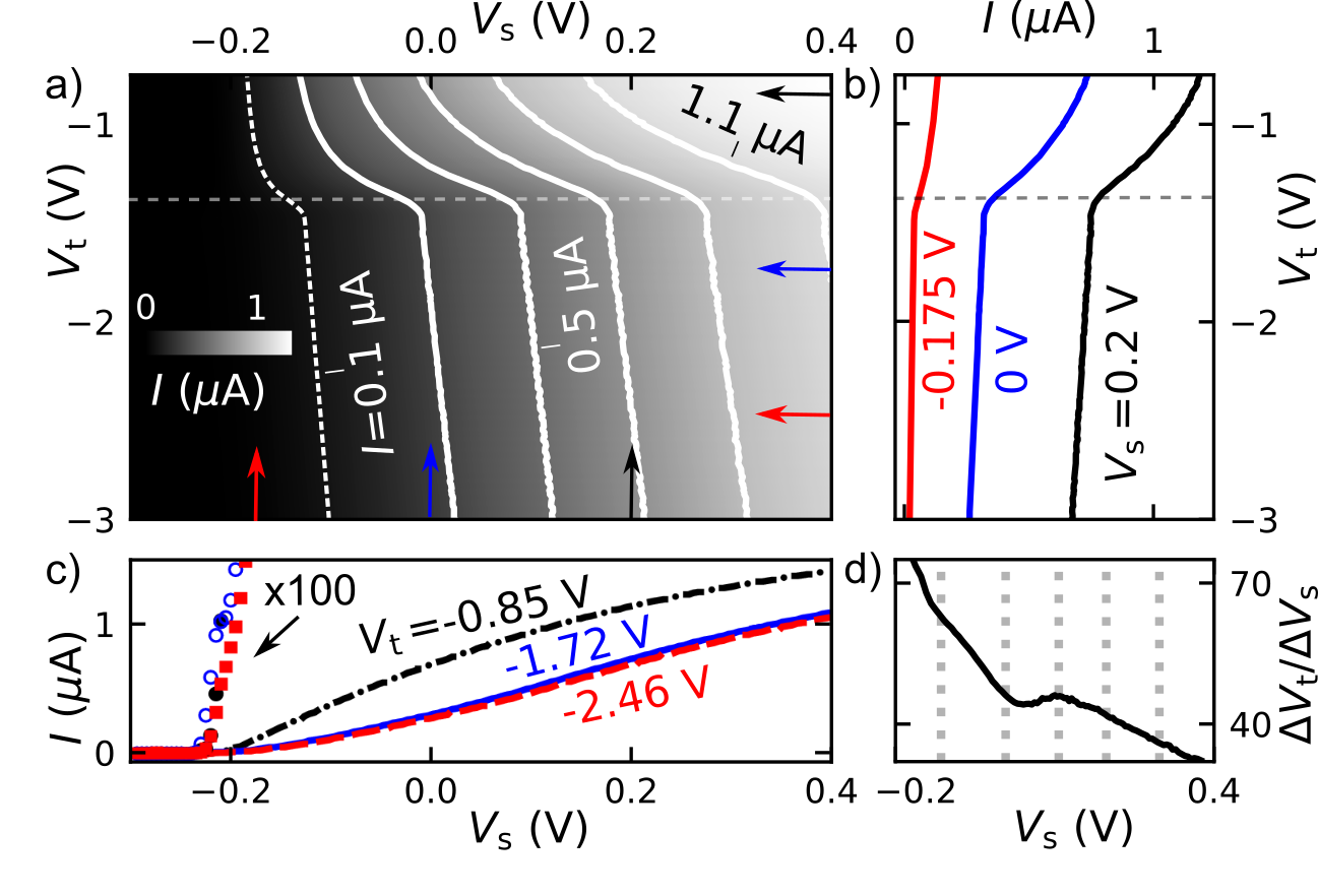
we present in Fig. 2 the current flowing between source and drain contacts (while the side contacts are left floating) in response to a source-drain voltage of mV as a function of both top gate and screen gate voltages and . The lines of constant current display a kink at V, marked by a dashed horizontal line in panels a) and b), indicating complete depletion of the 2DES for . The almost constant slope of each line of constant current for suggest, for a given value of , a constant ratio of the capacitances between the Hall-bar and the two respective gates, . To keep the current constant, a change in the screen gate voltage by can be compensated by a shift of the top gate voltage by . The value of quantifies the shielding of the influence of the top gate on the 2DES by the screen gate. It depends on the dielectric constants and geometry of the layers, which influence the electric field originating from the top gate. The coupling ratio, which we plot in Fig. 2(d) versus , takes the large value of at mV near depletion where it indicates an efficient screening of the top gate by the screen gate. The gradual increase to at mV indicates a growing influence of the top gate at more positive . Because the 2DES shaping the Hall-bar is the only variable component of our system, the observed reduction of the shielding effect, as is increased, indicates an increase of the Hall-bar width. Variations in the Hall-bar width, in turn, result in a rearrangement of the confinement potential perpendicular to the Hall-bar edges. Consequently, the combination of top- and screen gate voltages can be used to tune the steepness of the confinement at the Hall-bar edges which influence the shape and stability of quantum Hall edge states Siddiki et al. (2010). Reliable predictions could be achieved employing a Poison-Schrödinger solver such as nextnano3 Birner et al. (2007), while breakdown measurements of the quantum Hall effect would provide an experimental test Siddiki et al. (2010). Both ideas go beyond the scope of the present paper but are topics for the future.
To quantitatively evaluate the shielding, we compare the measured capacitance ratio with the ratio expected without screening , where denotes the capacitance between the top gate and the 2DES without the existence of a screen gate. For a first estimate we compare the measured depletion voltages of the respective gates . As a result, we find at V, i.e. the screen gate reduces the coupling of the top gate to the 2DES roughly by one order of magnitude. Clearly, this result depends on the geometry details and the applied voltages. The accuracy of the above numbers is around 10% reflecting the accuracy in determining the pinch-off voltages.
In a second approach we compare our first estimate based on direct measurements with the prediction of a simple plate capacitor model, assuming two separate plate capacitors, one between the top gate and the 2DES —but without screen gate— and the other between the screen gate and the 2DES. The model predicts , where the capacitor between the top gate and the 2DES contains two layers of dielectricum, nm of PMMA and nm of AlGaAs. We determine the required dielectric constant of our cross linked PMMA from our measured depletion voltage V of the top gate and the carrier density of the 2DES at grounded gates, , based on Hall measurements. Using our simple plate capacitor model, we find with being the vacuum permeability. Using the literature value Samara (1983) we find . Finally, our plate capacitor model predicts in fair agreement with our first estimate. From the equation above it is evident, that a thicker insulator layer between the screen gate and the top gate with a smaller dielectric constant would increase the screening effect.
III hall measurements: carrier density and mobility
We aim at evaluating the quality of the 2DES in nano circuits created with our method. Below we will use an Aharonov-Bohm ring for phase coherent measurements. However, first we measure carrier density and mobility based on the Hall-bar introduced above. As reference we use the “nominal” mobility and carrier density averaged over the wafer, which we measured directly after growth at the cryogenic temperature of K Wieck and Reuter (2000). They are V-1s-1 and , corresponding to a mean free path of m. In our sample we determine the carrier density (averaged over the width of the Hall-bar) by measuring the classical Hall voltage and the mobility by measuring the longitudinal resistance in the limit (), both at K. In Fig. 3
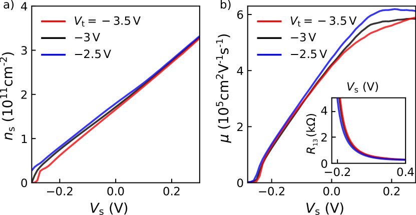
we present our results as a function of screen gate voltage and for various top gate voltages , i.e. where the 2DES beyond the Hall-bar is fully depleted and the Hall-bar is well defined. Both, the carrier density and mobility depend only little on the top gate voltage but are widely tunable by varying the screen gate voltage. For mV we observe a linear decrease of both, and , with decreasing indicating an approximately constant capacitance between 2DES and the screen gate and a resistivity (equivalent to ). We note, that gate voltage independent capacitances (as our ) between gates and the 2DES are not guaranteed as this property depends on the wafer material.
In our sample, at carrier density and mobility are reduced by approximately a factor of two compared to the “nominal” values of the pristine wafer. However the “nominal” values can be recovered by applying positive . This result suggests, that wafers with a higher doping level could be advantageous for applications requiring a high mobility or a highly tunable carrier density.
IV Aharonov-Bohm measurements: phase coherence
Our method offers a straightforward way to fabricate conducting pathways with ring topology. In Fig. 4

we present a photography of a sample containing seven quasi one-dimensional Aharonov-Bohm (AB) rings of various sizes and shapes in a parallel configuration connected to two-dimensional leads. The conductance of an individual ring can be measured by depleting the 2DES below the top gate and below all ring-shaped screen gates besides the one of the AB-ring of interest. To explore the phase coherence of the carriers, we here concentrate on the smallest ring (right most in Fig. 4) which is also presented as a scanning-electron microscope picture in Fig. 5(b).
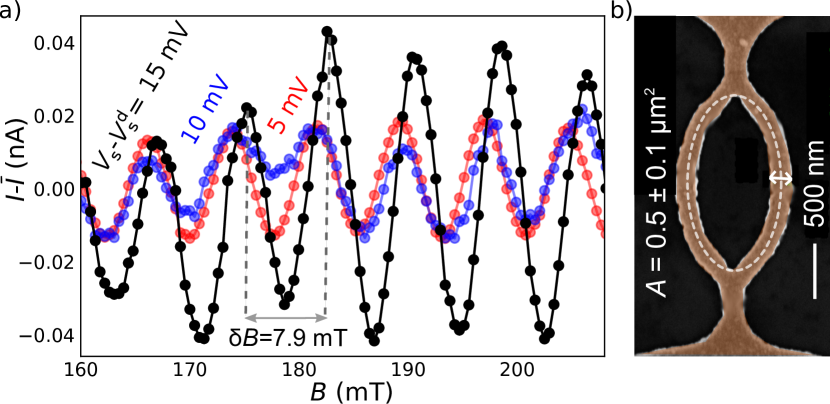
In Fig. 5(a) we present an example of AB oscillations, measured in a dilution refrigerator at a lattice temperature of 25 mK. Plotted is the current flowing through our ring in response to a source-drain voltage of mV versus the perpendicular magnetic field . The AB oscillations can be formally described as
| (1) |
where is the current averaged over , the visibility of the AB oscillations with amplitude and the area enclosed by the AB ring (which weakly depends on ). The first term contained in the cosine is times the number of enclosed magnetic flux quanta while sums up all other phase shifts which can be related to the existence of multiple paths (as for universal conductance fluctuations Ginossar et al. (2010); Ren et al. (2013); Castellanos-Beltran et al. (2013)) or geometry (such as the electrostatic AB effect van der Wiel et al. (2003)). The measured period of the AB oscillation in Fig. 5(a) of mT corresponds to the enclosed area of , coinciding with the area framed by the dashed line in Fig. 5(b).
In order to observe the AB-oscillations shown in Fig. 5(a) it was necessary to almost completely deplete the carriers in the AB-ring by applying close to the depletion voltage . This hints at a channel width so wide that it allows for multiple paths (in each arm) contributing with individual phases to the conductance which effectively reduces the visibility of the AB-oscillations Giesbers et al. (2010). As a rule of thumb, for our geometry an enclosed area difference of about 1% would suffice to generate a phase shift of at mT. The almost depleted ring sufficiently reduces the number of possible paths to reach a visibility of few percent. Taking the Hall-bar measurements above as a reference for the applied gate voltages we expect a carrier density of cm-2 and a mean free path in the order of m which is the same order of magnitude as the arm length of our AB-ring of m. However, screening is reduced along the almost depleted AB-ring, such that the mean-free-path could be shorter. Hence, we conclude that the electron dynamics in our AB-ring is located somewhere between the quasi-ballistic and the diffusive regime. One way to reach the ballistic regime in future devices will be to further reduce the intrinsic channel width such that quasi-one-dimensional channels can be realized at relatively large carrier densities. A further reduction of the screen gate width by a factor of four is easily achievable by electron-beam-lithography.
In Fig. 6(a)

we present AB-oscillations of the current as a function of and while in panel b we show an exemplary depletion curve plotting the current averaged over . The latter strongly oscillates as observed for Coulomb blockade oscillations, the current becomes small but stays finite in the Coulomb valleys. Such a behavior can be explained assuming two quantum dots in parallel Taylor et al. (1992), i.e. one dot in each arm of the AB-ring as indicated in the inset. The exact position of the quantum dots is thereby unknown. The overall resistance of at the two distinct current maxima below mV is in agreement with the assumption of two parallel dots giving rise to well established Coulomb blockade oscillations.
The two-terminal AB-oscillations in Fig. 6(a) feature (i) continuous phase shifts at finite , confirming the contribution of multiple paths in each arm, and (ii) phase jumps as a function of , confirming the existence of quantum dots in the arms of the AB-ring (phase jumps have been previously observed for one dot in one arm) Avinun-Kalish et al. (2005); Yacoby et al. (1996). Note that our ring is too small to explain the observed phase jumps by means of the electrostatic AB-effect van der Wiel et al. (2003).
In the following we will discuss the dephasing as a function of temperature and source-drain voltage. In an ideal two-terminal AB-ring composed of one-dimensional arms dephasing by energy broadening is absent at modest energies. The reason is phase rigidity Onsager (1931); Casimir (1945); Buttiker (1988); Yacoby et al. (1996); Kreisbeck et al. (2010) allowing only phase shifts by multiples of which would require either very different arm length or an unreasonably large energy window. Such an ideal AB-ring would be a perfect device to study the electron-electron interaction Washburn et al. (1985); Russo et al. (2008); Capron et al. (2013) remaining as possible dephasing process. However, realistic AB-rings as ours host multiple paths compromising the phase rigidity such that the temperature or source-drain voltage dependence of the dephasing at relatively small energies is dominated by energy broadening Cassé et al. (2000); Buchholz et al. (2010); Chung et al. (2005); Litvin et al. (2007). The measured temperature and source-drain voltage dependence of the visibility are presented in Fig. 7
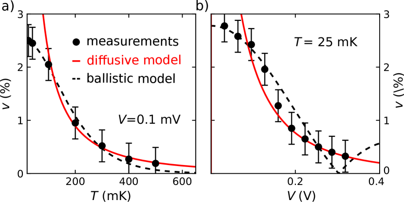
for mV where the two-terminal resistance is , compare Fig. 6(b). Having already established the existence of two parallel quantum dots we now consider two scenarios, namely either ballistic or diffusive transport between the quantum dots. Searching for an answer we fit the measured data in Fig. 7 for two idealistic models. The first one assumes diffusive transport in an AB-ring with quasi-one-dimensional arms for which the temperature dependence of the visibility has been obtained from the weak localization theory Washburn and Webb (1986)
| (2) |
with Treiber et al. (2009). This equation takes into account thermal broadening (square root term) and decoherence by scattering of electrons (exponential term). Here is the Thouless energy, the 2D diffusion constant and the electrons decoherence time. The according voltage dependence of the visibility derived from non-equilibrium dephasing models is Larkin and Khmel’nitskii (1986); Terrier et al. (2002)
| (3) |
with Gougam et al. (2000); DiVincenzo and Kane (1988). The prefactor takes into account that part of the source-drain voltage drops in the leads of the AB-ring. The red solid lines in Fig. 7 are fits to the respective temperature and voltage dependences given by Eq. (2) and Eq. (3). The diffusive model describes the measured data well for high energies but drastically overestimates the visibility at low or . This deviation can be explained with the approximations done in assuming for fitting the -dependence and for fitting the -dependence. The actual fit-parameters are listed in the caption of Fig. 7.
In our second idealistic scenario we assume ballistic transport through the AB-ring. Because the dwell time of an electron moving ballistically through the AB-ring is short compared to in this case we can neglect the influence of Nyquist noise which leaves energy broadening as only remaining dephasing process Treiber et al. (2009). Combining voltage and temperature dependence in first order the ballistic scenario can be described by Lin et al. (2010):
| (4) |
where defines the difference of the dwell times of a ballistic electron in the two arms of the AB-ring. A single fit to both data sets of Eq. (4) representing the ballistic model is shown as black dashed lines in Fig. 7. Our ballistic model describes the temperature dependence well but shows qualitative deviations in the voltage dependence (at high voltages). The actual fit-parameters are listed in the caption of Fig. 7. We find a dwell time difference of ps. On the one hand this corresponds to an unrealistically large arm length difference of m assuming ballistic motion at the Fermi velocity. On the other hand, the existence of a quantum dot in each arm leads to multiple reflections which would enhance dwell times. As a result, without further experimental and theoretical efforts it is impossible to determine from our data, whether transport through the AB ring is diffusive or ballistic. Diffusive transport might be caused by the almost complete depletion in the AB-rings which is necessary to reduce the number of one-dimensional channels preventing a higher visibility. We believe that AB-rings with narrower arms but higher carrier density will in future help to reach ballistic transport and to reduce the chance of the formation of quantum dots.
V conclusion
We have explored an alternative method to define mesoscopic circuits in heterostructures based on the electric field effect. The idea is to deplete most of the 2DES by means of a global top gate. Only at those areas where carriers are needed screen gates placed below the top gate are used to shield the effect of the top gate locally. The resulting circuits are highly tunable on the nanoscale as demonstrated in the presented experiments. Importantly, our method has the advantage of reducing the complexity of gate defined nanostructures. In more detail, it allows a straightforward way to realize conducting paths with ring topology and offers a way to define complex structures with a smaller number of gates compared to the conventional technology based on multiple depletion gates. Our Aharonov-Bohm measurements demonstrate phase coherence comparable to that in conventional AB-rings in semiconductors which makes our method suitable for quantum information applications. While not demonstrated here the closer vicinity of a metal gate to the carriers is expected to lead to a reduction of the Coulomb interaction between carriers. As such our method can be viewed as an alternative which will allow to increase the variety of physical properties in nanocircuits. Future tasks will include the definition of quantum point contacts and chains of quantum dots by using screen gates.
VI Acknowledgments
We thank P. Brouwer for fruitful discussions and are grateful for financial support from the DFG via LU 819/4-1.
References
- Behringer et al. (1987) R. E. Behringer, P. M. Mankiewich, and R. E. Howard, “Fabrication of ultrahigh resolution structures in compound semiconductor heterostructures,” Journal of Vacuum Science & Technology B: Microelectronics Processing and Phenomena 5, 326 (1987).
- Lee et al. (1989) K. Y. Lee, T. P. S. III, C. J. B. Ford, W. Hansen, C. M. Knoedler, J. M. Hong, and D. P. Kern, “Submicron trenching of semiconductor nanostructures,” Applied Physics Letters 55, 625 (1989), https://doi.org/10.1063/1.101805 .
- Ford et al. (1990) C. Ford, A. Fowler, J. Hong, C. Knoedler, S. Laux, J. Wainer, and S. Washburn, “Gated, asymmetric rings as tunable electron interferometers,” Surface Science 229, 307 (1990).
- Moon et al. (1998) E.-A. Moon, J.-L. Lee, and H. M. Yoo, “Selective wet etching of GaAs on AlGaAs for AlGaAs/InGaAs/AlGaAs pseudomorphic high electron mobility transistor,” Journal of Applied Physics 84, 3933 (1998).
- Held et al. (1998) R. Held, T. Vancura, T. Heinzel, K. Ensslin, M. Holland, and W. Wegscheider, “In-plane gates and nanostructures fabricated by direct oxidation of semiconductor heterostructures with an atomic force microscope,” Applied Physics Letters 73, 262 (1998).
- Heinzel et al. (2001) T. Heinzel, R. Held, S. Lüscher, K. Ensslin, W. Wegscheider, and M. Bichler, “Electronic properties of nanostructures defined in Ga[Al]As heterostructures by local oxidation,” Physica E: Low-dimensional Systems and Nanostructures 9, 84 (2001).
- Wieck and Ploog (1990) A. D. Wieck and K. Ploog, “In-plane-gated quantum wire transistor fabricated with directly written focused ion beams,” Applied Physics Letters 56, 928 (1990).
- Held et al. (1999) R. Held, S. Lüscher, T. Heinzel, K. Ensslin, and W. Wegscheider, “Fabricating tunable semiconductor devices with an atomic force microscope,” Applied Physics Letters 75, 1134 (1999).
- Platonov et al. (2015) S. Platonov, B. Kästner, H. W. Schumacher, S. Kohler, and S. Ludwig, “Lissajous rocking ratchet: Realization in a semiconductor quantum dot,” Phys. Rev. Lett. 115, 106801 (2015).
- Walukiewicz et al. (1984) W. Walukiewicz, H. E. Ruda, J. Lagowski, and H. C. Gatos, “Electron mobility in modulation-doped heterostructures,” Phys. Rev. B 30, 4571 (1984).
- Jung et al. (2004) S. W. Jung, T. Fujisawa, Y. Hirayama, and Y. H. Jeong, “Background charge fluctuation in a GaAs quantum dot device,” Applied Physics Letters 85, 768 (2004).
- Buizert et al. (2008) C. Buizert, F. H. L. Koppens, M. Pioro-Ladrière, H.-P. Tranitz, I. T. Vink, S. Tarucha, W. Wegscheider, and L. M. K. Vandersypen, “InSitu Reduction of Charge Noise in GaAs/AlGaAs Schottky-Gated Devices,” Phys. Rev. Lett. 101, 226603 (2008).
- Taubert et al. (2008) D. Taubert, M. Pioro-Ladrière, D. Schröer, D. Harbusch, A. S. Sachrajda, and S. Ludwig, “Telegraph noise in coupled quantum dot circuits induced by a quantum point contact,” Phys. Rev. Lett. 100, 176805 (2008).
- Schröer et al. (2007) D. Schröer, A. D. Greentree, L. Gaudreau, K. Eberl, L. C. L. Hollenberg, J. P. Kotthaus, and S. Ludwig, “Electrostatically defined serial triple quantum dot charged with few electrons,” Phys. Rev. B 76, 075306 (2007).
- Forster et al. (2015) F. Forster, M. Mühlbacher, D. Schuh, W. Wegscheider, G. Giedke, and S. Ludwig, “Multistability and spin diffusion enhanced lifetimes in dynamic nuclear polarization in a double quantum dot,” Phys. Rev. B 92, 245303 (2015).
- Buks et al. (1998) E. Buks, R. Schuster, M. Heiblum, D. Mahalu, and V. Umansky, “Dephasing in electron interference by a ’which-path’ detector,” Nature 391, 871 (1998).
- Chang et al. (2008) D.-I. Chang, G. L. Khym, K. Kang, Y. Chung, H.-J. Lee, M. Seo, M. Heiblum, D. Mahalu, and V. Umansky, “Quantum mechanical complementarity probed in a closed-loop Aharonov-Bohm interferometer,” Nat Phys 4, 205 (2008).
- Zailer et al. (1996) I. Zailer, J. E. F. Frost, V. Chabasseur-Molyneux, C. J. B. Ford, and M. Pepper, “Crosslinked PMMA as a high-resolution negative resist for electron beam lithography and applications for physics of low-dimensional structures,” Semiconductor Science and Technology 11, 1235 (1996).
- Teh and Smith (2003) W. H. Teh and C. G. Smith, “Fabrication of quasi-three-dimensional micro/nanomechanical components using electron beam cross-linked poly (methyl methacrylate) resist,” Journal of Vacuum Science & Technology B: Microelectronics and Nanometer Structures Processing, Measurement, and Phenomena 21, 3007 (2003).
- Note (1) Below this, there is a nm thick GaAs layer on top of periods of a superlattice of nm Al and nm As to stick segregating impurities during the MBE-growth at its interfaces and, thus, to keep the layers above clean. The 2DES is formed in the GaAs-layer close to the interface of the Al0.36Ga0.64As layer.
- Wieck and Reuter (2000) A. Wieck and D. Reuter, “High electron and hole mobility Al0.3Ga0.7As heterostructures grown in the same standard MBE setup,” Compound Semiconductors 1999: Proceedings of the 26th International Symposium on Compound Semiconductors, 23-26th August 1999, Berlin, Germany 22, 51 (2000).
- Ford et al. (1988) C. J. B. Ford, T. J. Thornton, R. Newbury, M. Pepper, H. Ahmed, C. T. Foxon, J. J. Harris, and C. Roberts, “The aharonov-bohm effect in electrostatically defined heterojunction rings,” Journal of Physics C: Solid State Physics 21, L325 (1988).
- Ford et al. (1989) C. J. B. Ford, T. J. Thornton, R. Newbury, M. Pepper, H. Ahmed, D. C. Peacock, D. A. Ritchie, J. E. F. Frost, and G. A. C. Jones, “Electrostatically defined heterojunction rings and the aharonov–bohm effect,” Applied Physics Letters 54, 21 (1989), https://doi.org/10.1063/1.100818 .
- Harrell et al. (1999) R. H. Harrell, K. S. Pyshkin, M. Y. Simmons, D. A. Ritchie, C. J. B. Ford, G. A. C. Jones, and M. Pepper, “Fabrication of high-quality one- and two-dimensional electron gases in undoped GaAs/AlGaAs heterostructures,” Applied Physics Letters 74, 2328 (1999).
- Chen et al. (2012) J. C. H. Chen, D. Q. Wang, O. Klochan, A. P. Micolich, K. D. Gupta, F. Sfigakis, D. A. Ritchie, D. Reuter, A. D. Wieck, and A. R. Hamilton, “Fabrication and characterization of ambipolar devices on an undoped AlGaAs/GaAs heterostructure,” Applied Physics Letters 100, 052101 (2012).
- Siddiki et al. (2010) A. Siddiki, J. Horas, D. Kupidura, W. Wegscheider, and S. Ludwig, “Asymmetric nonlinear response of the quantized Hall effect,” New Journal of Physics 12, 113011 (2010).
- Birner et al. (2007) S. Birner, T. Zibold, T. Andlauer, T. Kubis, M. Sabathil, A. Trellakis, and P. Vogl, “nextnano: General Purpose 3-D Simulations,” IEEE Transactions on Electron Devices 54, 2137 (2007).
- Samara (1983) G. A. Samara, “Temperature and pressure dependences of the dielectric constants of semiconductors,” Phys. Rev. B 27, 3494 (1983).
- Ginossar et al. (2010) E. Ginossar, L. I. Glazman, T. Ojanen, F. von Oppen, W. E. Shanks, A. C. Bleszynski-Jayich, and J. G. E. Harris, “Mesoscopic persistent currents in a strong magnetic field,” Phys. Rev. B 81, 155448 (2010).
- Ren et al. (2013) S. L. Ren, J. J. Heremans, C. K. Gaspe, S. Vijeyaragunathan, T. D. Mishima, and M. B. Santos, “Aharonov-Bohm oscillations, quantum decoherence and amplitude modulation in mesoscopic InGaAs/InAlAs rings,” Journal of Physics: Condensed Matter 25, 435301 (2013).
- Castellanos-Beltran et al. (2013) M. A. Castellanos-Beltran, D. Q. Ngo, W. E. Shanks, A. B. Jayich, and J. G. E. Harris, “Measurement of the Full Distribution of Persistent Current in Normal-Metal Rings,” Phys. Rev. Lett. 110, 156801 (2013).
- van der Wiel et al. (2003) W. G. van der Wiel, Y. V. Nazarov, S. De Franceschi, T. Fujisawa, J. M. Elzerman, E. W. G. M. Huizeling, S. Tarucha, and L. P. Kouwenhoven, “Electromagnetic Aharonov-Bohm effect in a two-dimensional electron gas ring,” Phys. Rev. B 67, 033307 (2003).
- Giesbers et al. (2010) A. J. M. Giesbers, U. Zeitler, M. I. Katsnelson, D. Reuter, A. D. Wieck, G. Biasiol, L. Sorba, and J. C. Maan, “Correlation-induced single-flux-quantum penetration in quantum rings,” Nat Phys 6, 173 (2010).
- Taylor et al. (1992) R. P. Taylor, A. S. Sachrajda, P. Zawadzki, P. T. Coleridge, and J. A. Adams, “Aharonov-Bohm oscillations in the Coulomb blockade regime,” Phys. Rev. Lett. 69, 1989 (1992).
- Avinun-Kalish et al. (2005) M. Avinun-Kalish, M. Heiblum, O. Zarchin, D. Mahalu, and V. Umansky, “Crossover from ’mesoscopic’ to ’universal’ phase for electron transmission in quantum dots,” Nature 436, 529 (2005).
- Yacoby et al. (1996) A. Yacoby, R. Schuster, and M. Heiblum, “Phase rigidity and h/2e oscillations in a single-ring Aharonov-Bohm experiment,” Phys. Rev. B 53, 9583 (1996).
- Onsager (1931) L. Onsager, “Reciprocal relations in irreversible processes. ii.” Phys. Rev. 38, 2265 (1931).
- Casimir (1945) H. B. G. Casimir, “On onsager’s principle of microscopic reversibility,” Rev. Mod. Phys. 17, 343 (1945).
- Buttiker (1988) M. Buttiker, “Symmetry of electrical conduction,” IBM Journal of Research and Development 32, 317 (1988).
- Kreisbeck et al. (2010) C. Kreisbeck, T. Kramer, S. S. Buchholz, S. F. Fischer, U. Kunze, D. Reuter, and A. D. Wieck, “Phase shifts and phase jumps in four-terminal waveguide Aharonov-Bohm interferometers,” Phys. Rev. B 82, 165329 (2010).
- Washburn et al. (1985) S. Washburn, C. P. Umbach, R. B. Laibowitz, and R. A. Webb, “Temperature dependence of the normal-metal Aharonov-Bohm effect,” Phys. Rev. B 32, 4789 (1985).
- Russo et al. (2008) S. Russo, J. B. Oostinga, D. Wehenkel, H. B. Heersche, S. S. Sobhani, L. M. K. Vandersypen, and A. F. Morpurgo, “Observation of Aharonov-Bohm conductance oscillations in a graphene ring,” Phys. Rev. B 77, 085413 (2008).
- Capron et al. (2013) T. Capron, C. Texier, G. Montambaux, D. Mailly, A. D. Wieck, and L. Saminadayar, “Ergodic versus diffusive decoherence in mesoscopic devices,” Phys. Rev. B 87, 041307 (2013).
- Cassé et al. (2000) M. Cassé, Z. D. Kvon, G. M. Gusev, E. B. Olshanetskii, L. V. Litvin, A. V. Plotnikov, D. K. Maude, and J. C. Portal, “Temperature dependence of the Aharonov-Bohm oscillations and the energy spectrum in a single-mode ballistic ring,” Phys. Rev. B 62, 2624 (2000).
- Buchholz et al. (2010) S. S. Buchholz, S. F. Fischer, U. Kunze, M. Bell, D. Reuter, and A. D. Wieck, “Control of the transmission phase in an asymmetric four-terminal Aharonov-Bohm interferometer,” Phys. Rev. B 82, 045432 (2010).
- Chung et al. (2005) V. S.-W. Chung, P. Samuelsson, and M. Büttiker, “Visibility of current and shot noise in electrical Mach-Zehnder and Hanbury Brown Twiss interferometers,” Phys. Rev. B 72, 125320 (2005).
- Litvin et al. (2007) L. V. Litvin, H.-P. Tranitz, W. Wegscheider, and C. Strunk, “Decoherence and single electron charging in an electronic Mach-Zehnder interferometer,” Phys. Rev. B 75, 033315 (2007).
- Washburn and Webb (1986) S. Washburn and R. A. Webb, “Aharonov-Bohm effect in normal metal quantum coherence and transport,” Advances in Physics 35, 375 (1986).
- Treiber et al. (2009) M. Treiber, O. M. Yevtushenko, F. Marquardt, J. von Delft, and I. V. Lerner, “Dimensional crossover of the dephasing time in disordered mesoscopic rings,” Phys. Rev. B 80, 201305 (2009).
- Larkin and Khmel’nitskii (1986) A. Larkin and D. E. Khmel’nitskii, “Mesoscopic fluctuations of current-voltage characteristics,” Journal of Experimental and Theoretical Physics 64, 1815 (1986).
- Terrier et al. (2002) C. Terrier, D. Babić, C. Strunk, T. Nussbaumer, and C. Schönenberger, “The amplitude of non-equilibrium quantum interference in metallic mesoscopic systems,” EPL (Europhysics Letters) 59, 437 (2002).
- Gougam et al. (2000) A. B. Gougam, F. Pierre, H. Pothier, D. Esteve, and N. O. Birge, “”Comparison of energy and phase relaxation in metallic wires”,” Journal of Low Temperature Physics 118, 447 (2000).
- DiVincenzo and Kane (1988) D. P. DiVincenzo and C. L. Kane, “Voltage fluctuations in mesoscopic metal rings and wires,” Phys. Rev. B 38, 3006 (1988).
- Lin et al. (2010) K.-T. Lin, Y. Lin, C. C. Chi, J. C. Chen, T. Ueda, and S. Komiyama, “Temperature- and current-dependent dephasing in an Aharonov-Bohm ring,” Phys. Rev. B 81, 035312 (2010).