Electric-field-induced extremely large change in resistance in graphene ferromagnets
Abstract
A colossal magnetoresistance () and an extremely large magnetoresistance () have been previously explored in manganite perovskites and Dirac materials, respectively. However, the requirement of an extremely strong magnetic field (and an extremely low temperature) makes them not applicable for realistic devices. In this work, we propose a device that can generate even larger changes in resistance in a zero-magnetic field and at a high temperature. The device is composed of a graphene under two strips of yttrium iron garnet (YIG), where two gate voltages are applied to cancel the heavy charge doping in the YIG-induced half-metallic ferromagnets. By calculations using the Landauer-Büttiker formalism, we demonstrate that, when a proper gate voltage is applied on the free ferromagnet, changes in resistance up to () can be achieved at the liquid helium (nitrogen) temperature and in a zero magnetic field. We attribute such a remarkable effect to a gate-induced full-polarization reversal in the free ferromagnet, which results in a metal-state to insulator-state transition in the device. We also find that, the proposed effect can be realized in devices using other magnetic insulators such as EuO and EuS. Our work should be helpful for developing a realistic switching device that is energy saving and CMOS-technology compatible.
I Introduction
Modern hard-drive read heads and magnetoresistance random access memories are based on a tunneling magnetoresistance effect in a multilayered magnetic tunneling junction structure Wolf et al. (2001); Žutić et al. (2004). The structure comprises one pinned and one free ferromagnets whose relative magnetization orientations can be switched between parallel and antiparallel configurations by an external magnetic field, yielding the desired low- and high-resistance states Chappert et al. (2007). About two decades ago, a colossal magnetoresistance (CMR) effect with a much larger on-off ratio () Jin et al. (1994), hence showing the possibility for a “next generation” computer hard drive, was found in multicomponent manganite perovskites Ramirez (1997). With decreasing temperature, the materials display a transition from a paramagnetic insulator to a ferromagnetic half-metal Satpathy et al. (1996); Park et al. (1998). Near the transition temperature, an external magnetic field can drive the insulator to a quasi-metal Ramirez (1997), yielding the “colossal” on-off ratios. A strong magnetic field is required for a relatively small low-resistance.
Several years ago, a colossal negative magnetoresistance was explored in functionalized graphene such as dilute fluorinated graphene Hong et al. (2011); Georgakilas et al. (2012). Very recently, an extremely large magnetoresistance (XMR) was explored in other Dirac materials. For example, unsaturated XMR up to at 4.5 K in a magnetic field of 14.7 T and XMR up to at 0.53 K in a magnetic field of 60 T were observed in WTe2 Ali et al. (2014), XMR of about one million percent at 2K and 9T was observed in LaSb Tafti et al. (2015), XMR of and at 2.5 K and 14 T were obtained in NbAs2 and TaAs2, respectively Wang et al. (2016), and unsaturated XMR up to at 1.8K in a magnetic field of 33 T was obtained in PtBi2 Gao et al. (2017). However, to achieve these CMR or XMR’s, extreme high-magnetic fields and low-temperatures are required. In these cases, it is not applicable for any realistic devices yet.
In this work, we propose a device that can generate even higher on-off ratios at a high temperature and in a zero magnetic field. The device is composed of a graphene under two strips of a magnetic insulator yttrium iron garnet (YIG), where two gate voltages are applied to cancel the heavy charge doping’s in the YIG-induced half-metallic ferromagnets (see Fig. 1(a)). Based on calculations using the Landauer-Büttiker formalism, we demonstrate that, by applying a proper voltage on one of the ferromagnets (the free one), an extremely large change in resistance up to can be achieved at the liquid helium temperature (4.2K) and in a magnetic filed of 0 T. The value maintains as at the liquid nitrogen temperature (77K). We indicate that, such huge on-off ratios stem from an electric-field-induced reversal of the full polarization in the free ferromagnet, which results in a transition between a metal and an insulator states in the device. Moreover, we find that, the proposed effect can be realized in graphene under two strips of other magnetic insulators, such as EuO and EuS.
II Device setup
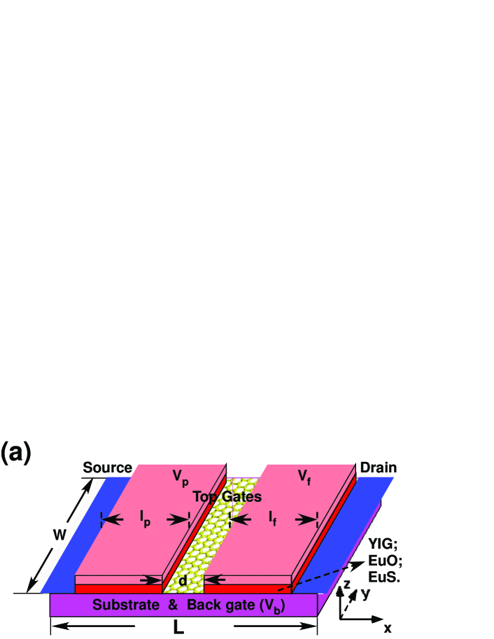
The designed device is shown in Fig. 1(a). A sufficiently wide (in the -direction) and short (in the -direction) graphene strip of is grown on a substrate. Here, is several times of to ensure that the transport is dominated by bulk states and does not depend on the edge types Tworzydło et al. (2006). On top of the graphene, two YIG strips of lengths and a distance are transferred Wang et al. (2015). As demonstrated by experiments Wang et al. (2015); Mendes et al. (2015); Leutenantsmeyer et al. (2016); Evelt et al. (2017) and first-principle calculations Hallal et al. (2017), the YIG strips induce ferromagnetism in the underlying graphene through an overlap of the spin-polarized Fe- states and the C states, which is called a magnetic proximity effect. The electronic structure of the graphene ferromagnet can be described by an exchange splitting for electrons or holes ( or ) and a band gap opening at the Dirac point (), see Fig. 2(b). Unfortunately, a heavy electron doping () is also induced in the graphene ferromagnet Wang et al. (2015); Hallal et al. (2017), which limits its spintronic application by a low polarization.
On the YIG strips two top gates () are placed Wang et al. (2015). They are used to cancel the heavy doping’s through a strong electric-field effect Wang et al. (2015) similar to that in pristine graphene Novoselov et al. (2004). The substrate under graphene is contacting a back gate (), which is used to tune the Fermi energy () through the whole device. When the Fermi energy is set as or , a half-metallic or normal ferromagnet of electron polarity is made use of. A small voltage () is further applied on the free ferromagnet to tune its Dirac point (). As we will see below, the Fermi energy and the Dirac point of the free ferromagnet are important to the states of the device. On the two sides of the device, the graphene film is contacted with a source and drain electrode, which may induce a contact doping () and a contact resistance Xia et al. (2011); Robinson et al. (2011); Song et al. (2012). Instead of YIG, EuO and EuS can be deposited on the graphene film. The ferromagnetism is induced by an overlap of the Eu states and the C states and all the parameters (, , ) Hallal et al. (2017) as well as the Curie temperatures () Wang et al. (2015); Swartz et al. (2012); Wei et al. (2016) become different. Here for YIG, EuO, and EuS, respectively.
| YIG/Gr | 550K | 0.78 | -5.8 | 11.6 | 0.63 | 2.6 | 5.3 | 0.70 |
|---|---|---|---|---|---|---|---|---|
| EuO/Gr | 69K | 1.37 | 4.2 | 13.4 | 1.337 | -2.4 | 9.8 | 1.628 |
| EuS/Gr | 16.5K | 1.3 | 1.6 | 18.3 | 1.40 | 0 | 15 | 1.70 |
III calculation formula
Below we will derive the formula to calculate the device conductance at different and . Devices using YIG, EuO, and EuS will be handled uniformly.
The low-energy dispersions around the Dirac points, which are predicted by first-principle calculations Hallal et al. (2017); Yang et al. (2013), are re-calculated and plotted in Fig. 2. The dispersions read
| (1) |
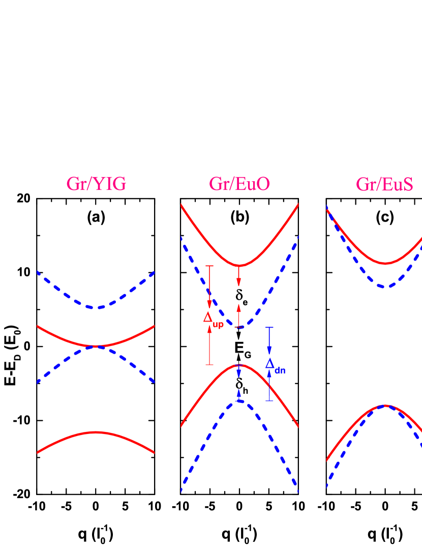
Here is the momentum, , , and ( for spin up and down) are the material- and spin-dependent Dirac cone dopings, Dirac gaps, and Fermi velocities, respectively. From Fig. 2, one can see clear spin-resolved parabolic dispersions, which accompany with a band gap opening at the Dirac point and exchange splitting’s for electrons and holes. The parameters for graphene on six trilayer YIG (six bilayer EuO and EuS) are given in Ref. Hallal et al. (2017). The parameters in Eq. (1) relate with them by and , see Fig. 2(b); are fitted from the original dispersions Hallal et al. (2017). The values are listed in table 1.
Regarding Eq. (1) as a combination of dispersions of two gapped graphene, the dispersions of the graphene ferromagnets can be described by an uniform effective Hamiltonian in a sublattice space Beenakker (2008)
| (2) |
where is the identity matrix, is the index for valley and , is the pseudospin Pauli matrices, and is the momentum operator. Such an effective Hamiltonian is different from those described in a sublattice-spin direct produce space Zollner et al. (2016); Su et al. (2017); Hallal et al. (2017), where the ferromagnets are viewed as a Dirac gap and two exchange splittings. Note, in this space a four-component wave function should be solved Song and Wu (2013). Different from them, in Eq. (2) we also consider a spin-resolved Fermi velocity . As we will show below, this parameter would determine an effective spin Dirac gap () hence play an important role in the insulator state. For the graphene under the electrode metals, , and for the pristine graphene between the pinned and free ferromagnets, , where is the potential shift.
When (the cases in Fig. 1 (b1) and (c1)), the right- and left-going envelope functions in the contacted, ferromagnetic, and pristine graphene () can be obtained by exactly resolved . Using a characteristic energy (length) meV ( nm), the dimensionless result reads
| (3) |
where , with for the pinned (free) ferromagnet, is the conserved transverse wave vector, , and with . It is seen that, . This means that, an effective spin Dirac gap, , is determined by not only the spin-dependent Dirac gap but also the spin-dependent Fermi velocity.
When (the cases in Fig. 1 (b2) and (c2)), the graphene between the ferromagnets becomes an n-p junction and the envelope function cannot be straightforwardly solved Sonin (2009); Song et al. (2013). Instead, the function can be solved in a pseudospin space which is rotated by around the -axis (see Fig. 1(a)) Sonin (2009); Song et al. (2013). The result reads
| (4) |
where and with being the Weber parabolic cylinder function and . Note, and [ and ] have the properties of a right (left)-going evanescent wave function Sonin (2009). In the rotated pseudospin space, the envelope functions for the contacted and ferromagnetic graphene become .
For , the ferromagnetisms hold and the inelastic scatterings (e-e and e-ph) can be ignored Morozov et al. (2008); Chen et al. (2008). The spin-resolved conductance through the device can be given by the Landauer-Büttiker formula Büttiker et al. (1985)
| (5) | ||||
where is a unit conductance, is a Fermi-Dirac distribution function, and is a spin-resolved transmission coefficient at a Dirac point of , an energy of , and an incident angle of . can be solved by with a standard transfer matrix method Born and Wolf (1980). The -dependent resistance of the device can be given by in unit of . The changes in resistance (RC) at different can be defined as
| (6) | ||||
To calculate a change in resistance, four conductance, and , should be calculated. Each of them depends strongly on the magnetic insulator (), ferromagnet length (), electrode contact (), Fermi energy (), and temperature ().
IV Results and discussion
IV.1 Gate-induced huge changes in resistance based on metal-insulator states
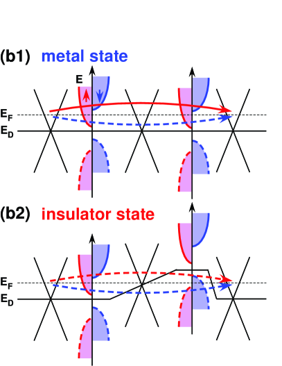
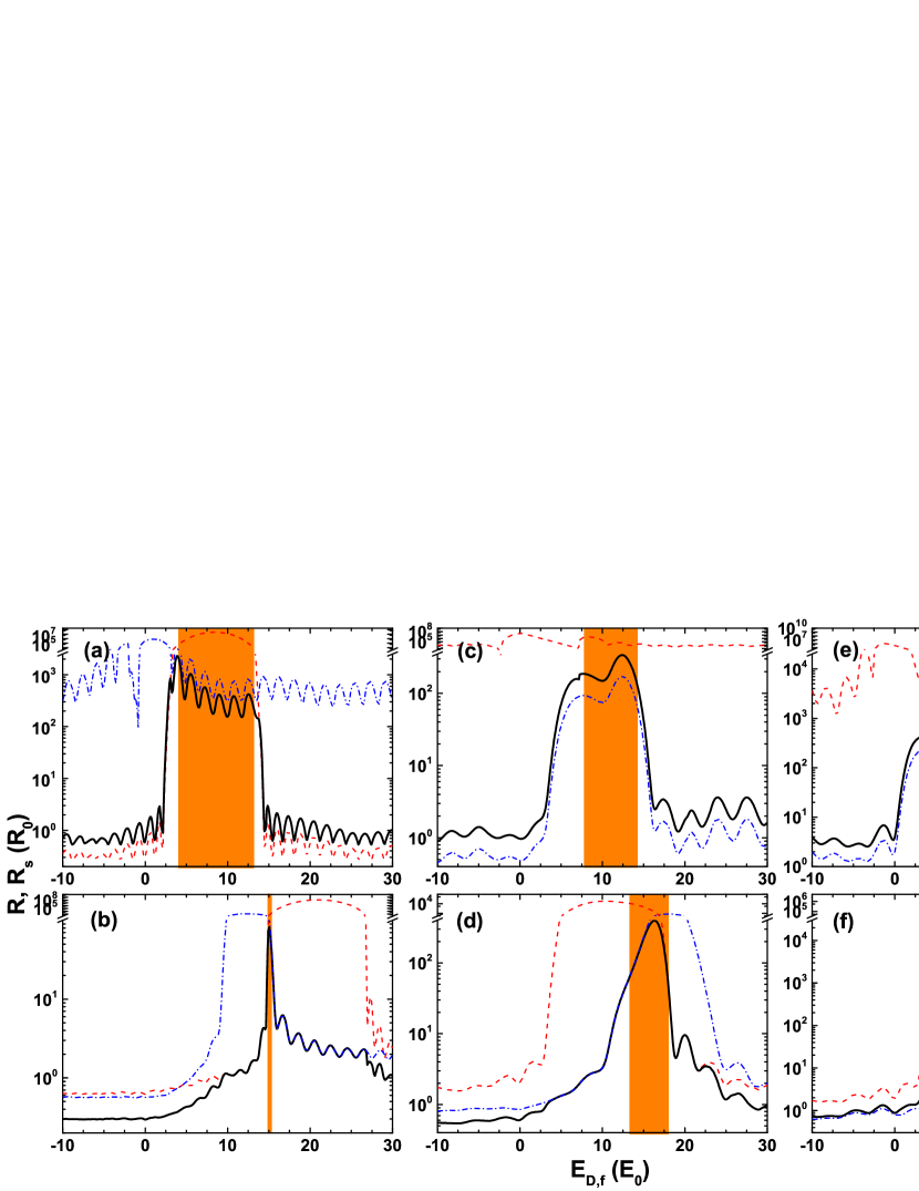
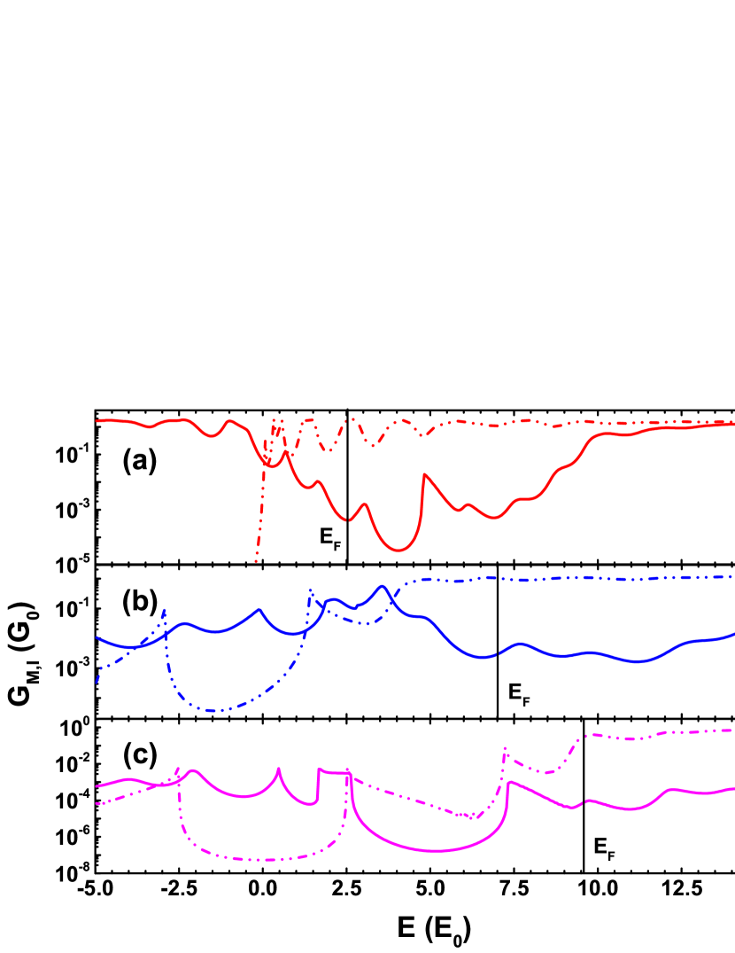
We first consider a YIG-based device with two half-metallic ferromagnets () of . Fig. 3(a) shows the zero-temperature device resistance as a function of . As can be seen, the device resistance is rather low () at ; it becomes rather high () as enters into the orange window. This leads to a huge on-off ratio of at . At , both ferromagnets are half-metallic (full polarizations of spin-up). Accordingly, electrons of spin up from the device source are transparent, while electrons of spin down are blocked by two potential barriers (see Fig. 1(b1)). These behaviors result in a near-unit transmission for spin up and a rather small transmission () for spin down, respectively, see the dashed lines in Fig. 4 (a). The transmissions respectively contribute a rather small () and large () resistance, see dashed lines in Fig. 3(a). The total resistance, as a parallel connection of them, is rather small (, almost equals to the small one). On the other hand, as can be seen in Fig. 5 (a), the low resistance increases with an increasing temperature, which implies that the device supports a metal state at .
In the orange window, and , see Fig. 2. The latter means that, the Fermi energy lies in the hole exchange splitting window of the free ferromagnet, see Fig. 1(b2). Importantly, the reversal of the charge polarity leads to an reversal of the spin polarization. In other words, by a proper the spin-up full polarization in the free ferromagnet becomes a spin-down full polarization. As a result, electrons of spin up from the device source, which are transparent before, now encounter a barrier in the free ferromagnet, On the other hand, electrons of spin down from the device source, which are blocked by two barriers before, now are still blocked by a barrier in the pinned ferromagnet (see Fig. 1(b2)). These behaviors are clearly reflected by the extremely suppressed transmissions () and rather high resistances ( and ) for both spins, as shown in Fig. 4 (a) and Fig. 3(a). The total resistance, as a parallel connection of two huge spin resistances, becomes rather high (). Besides the electric-field induced full-polarization reversal, the electric-field induced n-p junction also contributes to the high resistance state. This is because the transmissions become selective Cheianov and Fal ko (2006); Cheianov et al. (2007). In Fig. 5 (a), we find that the high resistance decreases with an increasing temperature, which implies that the device now supports an insulator state.
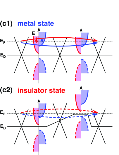
The resistances of the same device but with normal ferromagnets () are plotted in Fig. 3 (b) as a function of . Similar metal state at zero voltage and insulator state at a proper voltage are found. The resulting on-off ratio reads . However, it is noticed that, the range for the insulator state is different from that in Fig. 3(a) and it becomes much narrower. In the orange window, it is found that (), which means that, the Fermi energy enters into the Dirac gap of the free ferromagnet. As a result, electrons of both spins from the device source encounter potential barriers in the free ferromagnet, see Fig. 1(c2). This is clearly reflected by the rather small transmissions () and the rather high resistances ( and ) for both spins, see Fig. 4(b) and Fig. 3(b), respectively. The case is rather different from the zero voltage case, for which both spins transport over barriers (see Fig. 1(c1)) and result in near-unit transmissions in Fig. 4(b) and small resistances ( and ) in Fig. 3(b).
From the above results and discussions we can see that, colossal changes in resistance, which require a strong magnetic field in manganite perovskites, can be realized by a small gate voltage in the proposed device. The underlying mechanism is that, the gate induces either a full-polarization reversal in a half-metallic ferromagnet or an energy gap in a normal ferromagnet, which results in a metal-insulator state of the device. For the former case, the insulator state arises because different spins are blocked in different ferromagnets, while for the latter case, both spins are blocked in the free ferromagnet. The energy gap (1meV) is rather narrow and will be measured out at high temperature. In following we will focus on metal-insulator states stemming from the full-polarization reversal.
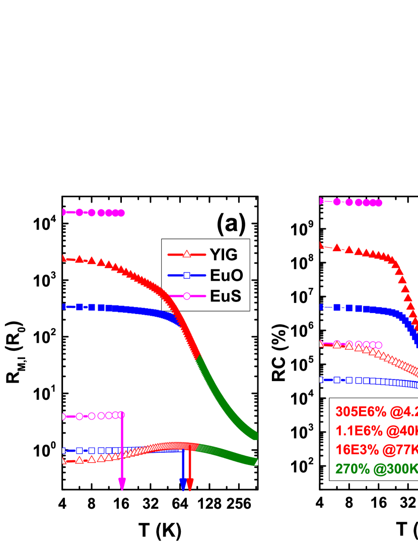
Can the remarkable effect be realized in other systems? In Fig. 3(c-f) we plot the calculation results for devices with ferromagnets induced by EuO and EuS. The half-metallic ferromagnet cases based on EuO () and EuS () are shown in Fig. 3(c) and (e), and the normal ferromagnet cases based on them () are shown in Fig. 3(d) and (f), respectively. It is seen that, the device resistance shows similar dependence on the Dirac point of the free ferromagnet as the YIG cases. The resulting CMR are , , , and for Figs. 3(c-f), respectively. Meanwhile, the low and high resistance at zero and proper show similar temperature dependence as the YIG cases (see Fig. 5(a)). The above behaviors mean that the voltage-induced metal-insulator states and huge changes in resistance can also be realized in devices based on other magnetic insulators.
IV.2 Ferromagnet-length dependence of the on-off ratios
In all the above calculations, the ferromagnet length is fixed as ; what will happen when it is changed? In Fig. 6(a) we plot the on-off ratio of the YIG-based device as a function of the lengths of the pinned and free ferromagnets. Surprisingly, it is found that, the on-off ratio is rather sensitive to the lengths; it shows a near-exponential dependence on the ferromagnet lengths excepting 11.5. When the ferromagnet lengths increase from 1 to 2, an extremely large on-off ratio up to arises.
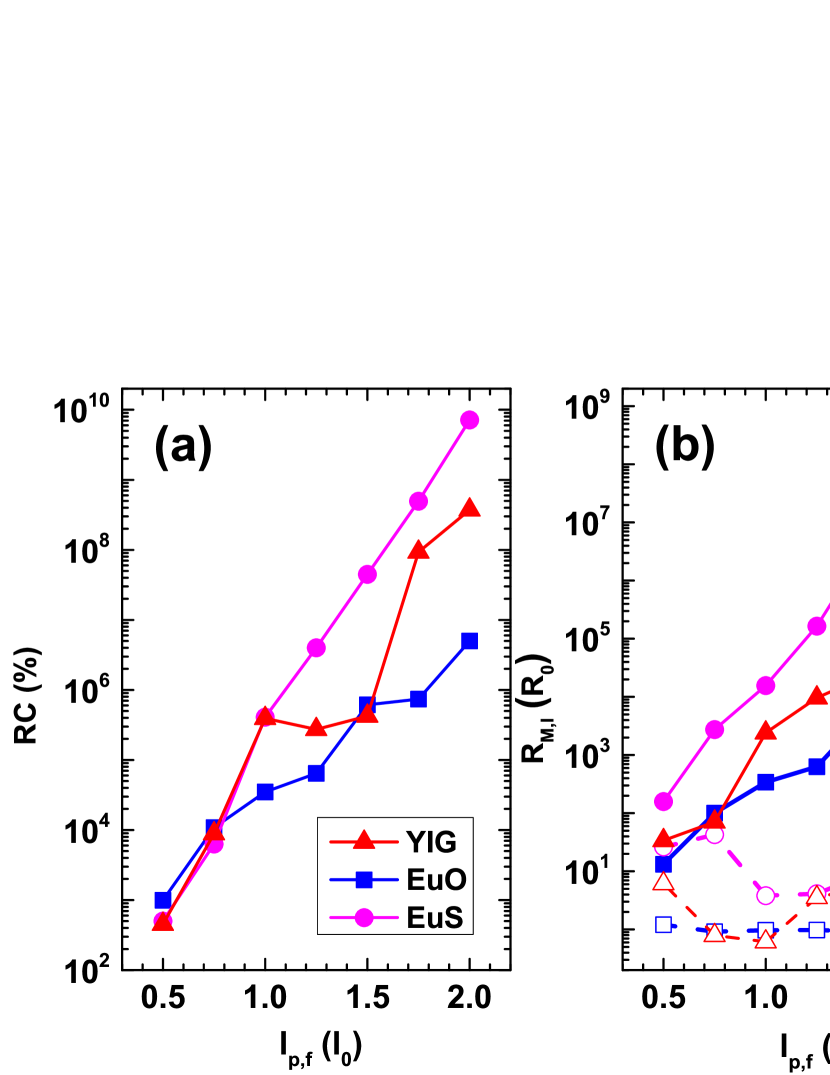
The strong enhancement can be understood as following. The insulator state of the device stems from evanescent transports of both spins, for which the longitudinal wave in Eq.(3) becomes an evanescent wave , where . As a result, the transmission and conductance decreases near-exponentially with an increasing barrier length. Hence, the resistance increases near-exponentially with an increasing length, see the red solid line in Fig. 6(b). In contrast, the metal state stems from a ballistic transport of spin up, for which is a plane wave. Accordingly, the transmission, conductance, and resistance show a weak oscillating dependence on the ferromagnet length, see the red dashed line in Fig. 6(b). The enhancement of the on-off ratio follows that of the insulator state.
The cases for devices using EuO and EuS are also plotted in Fig. 6. It is seen that, both the metal-insulator states and the on-off ratio show similar length dependence as the device using YIG. However, the slopes of the profiles are different. For the device using YIG, the change in resistance increases from at to at ; for the device using EuO, the on-off ratio changes from to , while for the device using EuS, the values read and . An enhancement factor, , can be calculated as 3, 2, and 4, respectively. Interestingly, they are found to be proportional to the squares of the smaller effective spin Dirac gaps (but not the smaller spin Dirac gap itself), i.e., . This is because the resistance is dominated by the spin with a smaller (i.e., spin down for all the three magnetic insulators, see table 1), and near the spin Dirac points.
IV.3 Temperature dependence of the changes in resistance
Till now, we only consider the zero-temperature on-off ratios. How it will change at high temperatures, especially at the liquid helium and the liquid nitrogen temperatures? In Fig. 5(b), we plot the numerical results for (the red solid line) as a function of temperature. As can be seen, the on-off ratio shows a decreasing dependence on the temperature, which is similar to the temperature dependence found in manganite perovskites and other Dirac materials. However, the on-off ratio maintains (18 smaller than the value at zero temperature) at the liquid helium temperature. This value is hundreds of times higher than the XMR previously reported in other Dirac materials at several K and under magnetic fields of several T Ali et al. (2014); Tafti et al. (2015); Wang et al. (2016); Gao et al. (2017). The change in resistance maintains as at the liquid nitrogen temperature, which is still comparable with the CMR observed in manganite perovskites at the same temperature and under magnetic fields of several T Jin et al. (1994). The Curie temperature of the YIG-induce graphene ferromagnet is higher than the room temperature. We have also calculated the on-off ratio at the room temperature by ignoring the inelastic scattering. A change in resistance of 270 is found. The temperature dependence for a device of is also shown, see the red dashed line in Fig. 5(b). It is found that, the on-off ratios are much smaller and the temperature dependence is much gentler. Moreover, the higher the temperature, the smaller the difference of the on-off ratios for different ferromagnet lengthes. It is noted that, the magnetic-field-induced CMR in manganite perovskites exists only near the zero-field transition temperature; the above results show that the proposed electric-field-induced extremely large on-off ratios can survive for a wide range of high temperature.
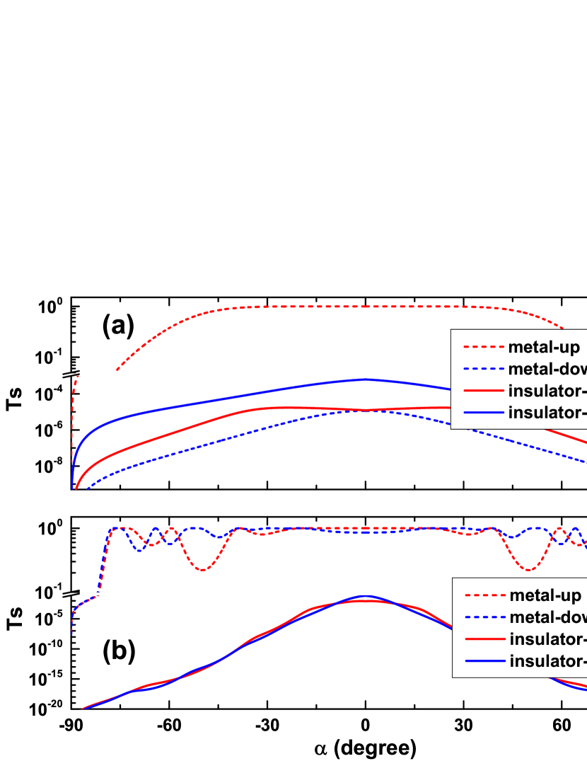
The decreasing temperature behavior of the on-off ratio stems from the increase behavior of the low-resistance state and the decrease behavior of the high-resistance state, which are also important evidences for a metal or insulator behavior. In following we will show that these behaviors stem from a negative and positive energy dependence of the zero-temperature conductance around the Fermi energy, respectively, see Fig. 7. Due to Eq. (5), a spin-dependent current at a finite temperature is determined by the zero-temperature currents in an estimated energy range . In Fig. 7 we plot the zero-temperature metal-insulator conductances () as a function of energy around the Fermi energy. As can be seen, reaches almost the maximum (minimum) around the Fermi energy, which are direct results of the electronic structure as shown in Fig. 2. Accordingly, the higher the temperature, i.e., the wider the energy range, the smaller (bigger) the finite-temperature and . An abnormal decreasing of above K is also observed. It stems from a “W”-shaped - profile.
IV.4 Metal contacting effects
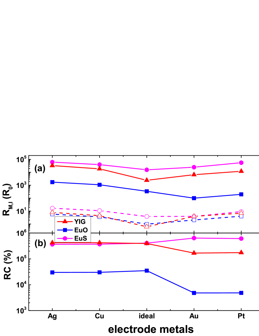
At last, we consider the influence of metal contacts on the changes in resistance. Several familiar metals, Ag, Cu, Au, and Pt at their equilibrium distances with graphene are considered. The contact doping’s () equal -32, -17, 19, and 32, respectively Giovannetti et al. (2008). The calculated results are shown in Fig. 8. It is observed that, for device using YIG and EuS, both and increase as the contacts become non-ideal; the heavier the contact doping, the larger the resistances increase. This is because the contacting resistances are in series with the original ones. However, the low and high resistances increase differently. As a result, the on-off ratio can show different behaviors. It decreases for device using YIG (EuS) with positive (negative) doping’s, while increases for device using YIG (EuS) with negative (positive) doping’s. Considering that the contact resistance is usually harmful for device performance Russo et al. (2010), the latter is a rather interesting and useful result. For device using EuO, the change in resistance always decreases, slightly for negative contact doping’s and sharply for positive contact doping’s.
V Conclusion
In summary, we have proposed a device that can generate extremely large changes in resistance at high temperatures and in a zero magnetic field. The device is composed of a graphene under two YIG strips, where gate voltages are applied. Based on conductance calculations we have demonstrated that, by applying a proper gate on the free ferromagnet, an on-off ratio up to can be obtained at the liquid helium temperature and in a zero magnetic field. This value is hundreds of times higher than the XMR previously observed in Dirac materials at similar temperatures and under magnetic fields of several T. The change in resistance maintains as at the liquid nitrogen temperature and in a zero magnetic field, which is still comparable with the CMR observed in manganite perovskites at the same temperature and under magnetic fields of several T. We have indicated that, the underlying mechanism for such a remarkable effect is that, an electric field induces a reversal of the full polarization in the half-metallic free ferromagnet, which results in metal-insulator states in the device.
Interesting results also contain: 1) the change in resistance shows a near-exponential dependence on the ferromagnet lengths, 2) the longer the two ferromagnets, the sharper the negative temperature-dependence of the on-off ratio, and 3) the effective spin Dirac gap instead of the spin Dirac gap itself plays an important role in the insulator state. We have also shown that, the proposed effect can be realized in devices using other magnetic insulators such as EuO and EuS. Our work should be helpful for developing a realistic switching device. Using an electric field instead of a magnetic field, the proposed device is also far more energy saving and compatible with the ubiquitous voltage-controlled semiconductor technology Chiba et al. (2008); Ohno (2010); Matsukura et al. (2015).
Acknowledgements
I’d like to thank M.S. XL Feng and Dr. SY Hou for inspiring discussions. This work was supported by the National Natural Science Foundation of China (Grant No. 11404300) and the Science Challenge Project (Grant No. TZ2016003-1).
References
- Wolf et al. (2001) S. Wolf, D. Awschalom, R. Buhrman, J. Daughton, S. Von Molnar, M. Roukes, A. Y. Chtchelkanova, and D. Treger, Science 294, 1488 (2001).
- Žutić et al. (2004) I. Žutić, J. Fabian, and S. D. Sarma, Rev. Mod. Phys. 76, 323 (2004).
- Chappert et al. (2007) C. Chappert, A. Fert, and F. N. Van Dau, Nature Mater. 6, 813 (2007).
- Jin et al. (1994) S. Jin, T. Tiefel, M. McCormack, R. Fastnacht, R. Ramesh, and L. Chen, Science 264, 413 (1994).
- Ramirez (1997) A. Ramirez, J. Phys. Condens. Matter. 9, 8171 (1997).
- Satpathy et al. (1996) S. Satpathy, Z. S. Popović, and F. R. Vukajlović, Phys. Rev. Lett. 76, 960 (1996).
- Park et al. (1998) J.-H. Park, E. Vescovo, H.-J. Kim, C. Kwon, R. Ramesh, and T. Venkatesan, Nature 392, 794 (1998).
- Hong et al. (2011) X. Hong, S.-H. Cheng, C. Herding, and J. Zhu, PHYSICAL REVIEW B 83, 085410 (2011).
- Georgakilas et al. (2012) V. Georgakilas, M. Otyepka, A. B. Bourlinos, V. Chandra, N. Kim, K. C. Kemp, P. Hobza, R. Zboril, and K. S. Kim, Chemical Reviews 112, 6156 (2012).
- Ali et al. (2014) M. Ali, J. Xiong, S. Flynn, J. Tao, Q. Gibson, L. Schoop, T. Liang, N. Haldolaarachchige, M. Hirschberger, N. Ong, and R. Cava, Nature 514, 205 (2014).
- Tafti et al. (2015) F. Tafti, Q. Gibson, S. Kushwaha, N. Haldolaarachchige, and R. Cava, Nature Phys. 12, 272 (2015).
- Wang et al. (2016) Y.-Y. Wang, Q.-H. Yu, P.-J. Guo, K. Liu, and T.-L. Xia, Phys. Rev. B 94, 041103 (2016).
- Gao et al. (2017) W. Gao, N. Hao, F.-W. Zheng, W. Ning, M. Wu, X. Zhu, G. Zheng, J. Zhang, J. Lu, H. Zhang, et al., Phys. Rev. Lett. 118, 256601 (2017).
- Tworzydło et al. (2006) J. Tworzydło, B. Trauzettel, M. Titov, A. Rycerz, and C. W. J. Beenakker, Phys. Rev. Lett. 96, 246802 (2006).
- Wang et al. (2015) Z. Wang, C. Tang, R. Sachs, Y. Barlas, and J. Shi, Phys. Rev. Lett. 114, 016603 (2015).
- Mendes et al. (2015) J. Mendes, O. A. Santos, L. Meireles, R. Lacerda, L. Vilela-Leão, F. Machado, R. Rodríguez-Suárez, A. Azevedo, and S. Rezende, Phys. Rev. Lett. 115, 226601 (2015).
- Leutenantsmeyer et al. (2016) J. C. Leutenantsmeyer, A. A. Kaverzin, M. Wojtaszek, and B. J. van Wees, 2D Mater. 4, 014001 (2016).
- Evelt et al. (2017) M. Evelt, H. Ochoa, O. Dzyapko, V. E. Demidov, A. Yurgens, J. Sun, Y. Tserkovnyak, V. Bessonov, A. B. Rinkevich, and S. O. Demokritov, Phys. Rev. B 95, 024408 (2017).
- Hallal et al. (2017) A. Hallal, F. Ibrahim, H. Yang, S. Roche, and M. Chshiev, 2D Mater. 4, 025074 (2017).
- Novoselov et al. (2004) K. S. Novoselov, A. K. Geim, S. V. Morozov, D. Jiang, Y. Zhang, S. V. Dubonos, I. V. Grigorieva, and A. A. Firsov, Science 306, 666 (2004).
- Xia et al. (2011) F. Xia, V. Perebeinos, Y.-m. Lin, Y. Wu, and P. Avouris, Nature Nanotech. 6, 179 (2011).
- Robinson et al. (2011) J. A. Robinson, M. LaBella, M. Zhu, M. Hollander, R. Kasarda, Z. Hughes, K. Trumbull, R. Cavalero, and D. Snyder, Appl. Phys. Lett. 98, 053103 (2011).
- Song et al. (2012) S. M. Song, J. K. Park, O. J. Sul, and B. J. Cho, Nano Lett. 12, 3887 (2012).
- Swartz et al. (2012) A. G. Swartz, P. M. Odenthal, Y. Hao, R. S. Ruoff, and R. K. Kawakami, ACS Nano 6, 10063 (2012).
- Wei et al. (2016) P. Wei, S. Lee, F. Lemaitre, L. Pinel, D. Cutaia, W. Cha, F. Katmis, Y. Zhu, D. Heiman, J. Hone, et al., Nature Mater. 15, 711 (2016).
- Yang et al. (2013) H.-X. Yang, A. Hallal, D. Terrade, X. Waintal, S. Roche, and M. Chshiev, Phys. Rev. Lett. 110, 046603 (2013).
- Beenakker (2008) C. Beenakker, Rev. Mod. Phys. 80, 1337 (2008).
- Zollner et al. (2016) K. Zollner, M. Gmitra, T. Frank, and J. Fabian, Phys. Rev. B 94, 155441 (2016).
- Su et al. (2017) S. Su, Y. Barlas, J. Li, J. Shi, and R. K. Lake, Phys. Rev. B 95, 075418 (2017).
- Song and Wu (2013) Y. Song and H.-C. Wu, J. Phys. Condens. Matter. 25, 355301 (2013).
- Sonin (2009) E. Sonin, Phys. Rev. B 79, 195438 (2009).
- Song et al. (2013) Y. Song, H.-C. Wu, and Y. Guo, Appl. Phys. Lett. 102, 093118 (2013).
- Morozov et al. (2008) S. Morozov, K. Novoselov, M. Katsnelson, F. Schedin, D. Elias, J. A. Jaszczak, and A. Geim, Phys. Rev. Lett. 100, 016602 (2008).
- Chen et al. (2008) J.-H. Chen, C. Jang, S. Xiao, M. Ishigami, and M. S. Fuhrer, Nature Nanotech. 3, 206 (2008).
- Büttiker et al. (1985) M. Büttiker, Y. Imry, R. Landauer, and S. Pinhas, Phys. Rev. B 31, 6207 (1985).
- Born and Wolf (1980) M. Born and E. Wolf, Principles of optics: electromagnetic theory of propagation, interference and diffraction of light (Elsevier, 1980).
- Cheianov and Fal ko (2006) V. V. Cheianov and V. I. Fal ko, Phys. Rev. B 74, 041403 (2006).
- Cheianov et al. (2007) V. V. Cheianov, V. Fal’ko, and B. Altshuler, Science 315, 1252 (2007).
- Giovannetti et al. (2008) G. Giovannetti, P. Khomyakov, G. Brocks, V. v. Karpan, J. Van den Brink, and P. Kelly, Phys. Rev. Lett. 101, 026803 (2008).
- Russo et al. (2010) S. Russo, M. Craciun, M. Yamamoto, A. Morpurgo, and S. Tarucha, Phys. E 42, 677 (2010).
- Chiba et al. (2008) D. Chiba, M. Sawicki, Y. Nishitani, Y. Nakatani, F. Matsukura, and H. Ohno, Nature 455, 515 (2008).
- Ohno (2010) H. Ohno, Nature Mater. 9, 952 (2010).
- Matsukura et al. (2015) F. Matsukura, Y. Tokura, and H. Ohno, Nature Nanotech. 10, 209 (2015).