Room-temperature spin transport in -Ge probed by four-terminal nonlocal measurements
Abstract
We demonsrtate electrical spin injection and detection in n-type Ge (n-Ge) at room temperature using four-terminal nonlocal spin-valve and Hanle-effect measurements in lateral spin-valve (LSV) devices with Heusler-alloy Schottky tunnel contacts. The spin diffusion length (Ge) of the Ge layer used ( 1 1019 cm-3) at 296 K is estimated to be 0.44 0.02 m. Room-temperature spin signals can be observed reproducibly at the low bias voltage range ( 0.7 V) for LSVs with relatively low resistance-area product () values ( 1 km2). This means that the Schottky tunnel contacts used here are more suitable than ferromagnet/MgO tunnel contacts ( 100 km2) for developing Ge spintronic applications.
Owing to the future intrinsic limits of downsizing of silicon-based conventional complementary metal-oxide-semiconductor (CMOS) transistors, novel devices with additional functionalities should be developed. Spin-based electronics (spintronics) is expected to enhance device performances because of its nonvolatility, reconstructibility, low power consumption, and so forth.Igor ; Hirohata ; Taniyama ; Yuasa ; Tanaka To introduce the use of spintronics into the Si-based semiconductor industry, it will become important to explore spintronic technologies compatible with Si.Jansen1 ; Appelbaum ; Jonker ; Si_HamaGr ; Suzuki ; Ishikawa In recent years, germanium has been attracting much attention as a channel material for next-generation CMOS transistors because its electron and hole mobility are twice and four times as large as those in Si, respectively.Kuzum ; Zhang1
In line with this research, there have been many studies to date on the development of spintronic technologies using Ge.Zhou ; KAIST ; Ge_Hama1 ; Ge_Hama2 ; Ge_Hama3 ; AIST ; Jamet For heavily doped n-Ge (1018 cm-3 1019 cm-3), the spin diffusion length (Ge) at room temperature, one of the key parameters in Ge spintronics, has been reported by some experimental methods. First, the value of Ge at room temperature was estimated to be 0.68 m from three-terminal Hanle-effect measurements of CoFe/MgO/n-Ge devices.KAIST Next, by analyzing the detected inverse-spin-Hall voltage in Py/n-Ge/Pd devices, a room-temperature Ge value of 0.66 m was expected,Dushenko_PRL which is similar to that in Ref. KAIST . However, there is no report on the room-temperature Ge estimated from four-terminal nonlocal spin-valve and Hanle-effect measurements although this is the most reliable method for exploring spin transport in nonmagnets.Johnson ; Jedema ; Kimura ; Lou_NatPhys
Here, we report on room-temperature four-terminal nonlocal spin signals and Hanle-effect curves obtained under parallel and anti-parallel magnetization configurations of Co2FeAl (CFA) Schottky tunnel contacts in n-Ge-based lateral spin-valves (LSVs). This means that generation, manipulation, and detection of pure spin currents in n-Ge are reliably demonstrated at room temperature by all-electrical means for the first time. The Ge value of the n-Ge layer used here ( 1 1019 cm-3) is estimated to be 0.44 0.02 m. Room-temperature spin signals can be observed for LSVs with relatively low resistance-area product () values ( 1 km2), which are much lower than that of ferromagnet/MgO tunnel contacts in the low bias voltage range in room-temperature Ge spintronics.KAIST ; Jamet This study will pave a way to develop spintronic applications with Ge technologies.
First, the growth of Ge layers used in this study for spin transport is explained. We formed an undoped Ge(111) layer (28 nm) grown at 350 ∘C (LT-Ge) on a commercial undoped Si(111) substrate ( 1000 cm), followed by an undoped Ge(111) layer (70 nm) grown at 700 ∘C (HT-Ge).Sawano_TSF As the spin transport layer, we grew a 140-nm-thick phosphorous (P)-doped -Ge(111) layer (doping concentration 1019 cm-3) by molecular beam epitaxy (MBE) at 350 ∘C on top of the HT-Ge layer. The carrier concentration () in the -Ge(111) layer was estimated to be 1 1019 cm-3. Because the HT-Ge layer on LT-Ge/Si(111) has -type conduction and a relatively high resistivity (high spin resistance) compared to the spin transport (-Ge) layer, we can ignore the spin diffusion into the HT-Ge layer. To promote the tunneling conduction of electron spins through the Schottky barriers,Ge_Hama2 ; Ge_Hama1 ; Ge_Hama3 a P -doped Ge layer (-Ge) with an ultra thin Si insertion layer was grown on top of the spin-transport layer.MYamada As the spin injector/detector, we used Co2FeAl (CFA) grown by low-temperature MBE because it is relatively simple to grow compared to Co2FeAl0.5Si0.5, which was previously reported in Ref. Ge_Hama3 . Here CFA is also expected to exhibit relatively high spin polarization.Sukegawa Detailed growth procedures have been published elsewhere.SYamada
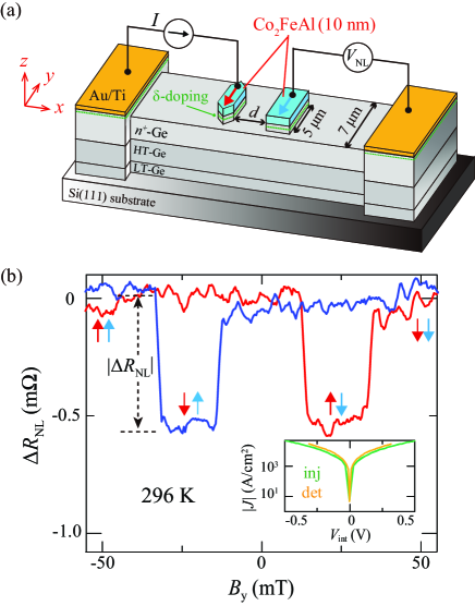
Figure 1(a) shows a schematic illustration of the fabricated LSVs for four-terminal nonlocal measurements.Johnson ; Jedema ; Kimura Two different CFA/-Ge contacts with 0.4 5.0 m2 and 1.0 5.0 m2 in size were fabricated by conventional electron beam lithography and Ar-ion milling. The edge-to-edge distances between the CFA/-Ge contacts were measured to be 0.24 to 0.55 m. Representative current-voltage characteristics ( curves) of the fabricated CFA/-Ge Schottky tunnel contacts are shown in the inset of Fig. 1(b). Because there is no rectifying behavior, we can judge that the tunneling conduction of electrons through the CFA/-Ge interfaces is demonstrated irrespective of the influence of the strong Fermi level pinning at the metal/-Ge interface.Dimoulas By applying in-plane magnetic fields (y), four-terminal nonlocal magnetoresistance (NL NL/) curves are measured at = -2 mA at room temperature (296 K), as shown in the main panel of Fig. 1(b). Here the negative sign of ( 0) means that spin-polarized electrons are injected from CFA into -Ge. Evident hysteretic behavior of , depending on the magnetization configuration between the two CFA contacts, can be observed even at room temperature. These features can be reproducibly observed in many LSVs, as shown in the discussion below. For the presented LSV ( 0.24 m), the amplitude of the spin signal, , is approximately 0.54 m at room temperature.
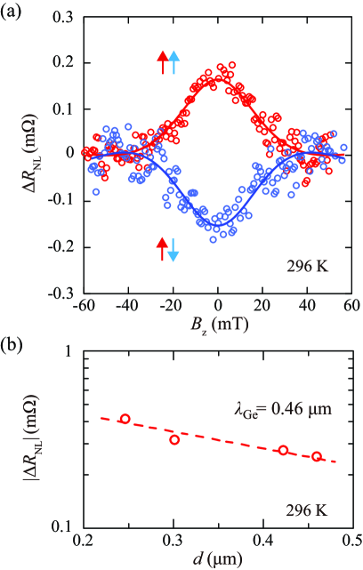
By applying out-of-plane magnetic fields (z), we also measure four-terminal nonlocal Hanle-effect curves under parallel and anti-parallel magnetization states between the CFA electrodes. In Fig. 2(a), we can see clearly nonlocal Hanle-effect curves, indicating precession of the pure spin currents in the n-Ge layer at room temperature, for both the parallel and antiparallel magnetization states in an LSV having 0.5 m. This is the first observation of four-terminal nonlocal Hanle-effect curves at room temperature in n-Ge, that were detected entirely by electrical means. According to the one-dimensional spin drift diffusion model,Lou_NatPhys ; Jedema the four-terminal nonlocal Hanle-effect curves can be expressed as follows.
| (1) |
where , , L (= Bz/) is the Larmor frequency, is the electron -factor ( = 1.56) of Ge,Vrijen B is the Bohr magneton, and are the spin polarizations of electrons in n-Ge, is the resistivity ( 1.9 mcm), is the cross section ( 0.98 m2) of the n-Ge layer used here, and is the center-to-center distance between the spin injector and detector ( 1.2 m). The solid curves presented in Fig. 2(a) indicate the results fitted to Eq.(1). In consequence, the Ge and values are determined to be 0.25 ns and 7.2 cm2/s, respectively. Here the influence of the contact-induced spin relaxation on the Hanle analysis of our LSVs can be ignored because the Ge value obtained using Eq. (5) in Ref. Brien_PRB was nearly equivalent to that obtained using Eq. (1). In addition, according to the relation , we can calculate a value of 0.42 m at room temperature for the -Ge layer used here. In Fig. 2(b), we also investigate the dependence of for evaluating using the following equation, . Here we use LSVs other than that shown in Fig. 2(a) because we should confirm the reliability of the value estimated from the same-Ge layer. As a result, we can obtain a value of 0.46 m. From both the Hanle effect and dependence analyses, we regard at room temperature as 0.44 0.02 m, which is slightly different from the values obtained in previous room-temperature works.KAIST ; Dushenko_PRL
Recently, by utilizing a Co-based Heusler alloy as a spin injector and detector, we have obtained large and reliable spin signals at low temperatures and gained insight into the spin relaxation mechanism in n-Ge from low temperature to near room temperature.Ge_Hama3 Theoretical analyses revealed that the spin relaxation mechanism in n-Ge (1018 cm-3 1019 cm-3) at low temperatures is dominated by donor-driven intervalley spin-flip scattering.Ge_Hama3 ; Song_PRL It should be noted that, however, at room temperature, the phonon-induced intervalley spin-flip scattering cannot be ignored.Ge_Hama3 Considering both contributions to Ge, we can theoretically calculate a room temperature Ge value of 0.2 ns,Ge_Hama3 which leads to a of 0.45 m. The experimentally obtained data in this study ( 0.44 0.02 m) are consistent with the above theoretical value. In terms of the theoretical spin relaxation mechanism,Song_PRL the estimated value in this study is more reliable than those estimated by other methods.KAIST ; Dushenko_PRL
A comparison of and at room temperature shows that the obtained is obviously smaller than the reported ( 1.0 m).Ishikawa For both Ge and Si, although the spin relaxation mechanism is dominated by the donor-driven and phonon-induced intervalley spin-flip scattering predicted theoreticallySong_PRL and experimentally,Ge_Hama3 ; Ishikawa the contributions of the Bohr radius and spin-orbit coupling in Ge to the spin scattering rate are relatively large compared to those in Si. Therefore, reducing the donor concentration in n-Ge might be important to enhance at room temperature in future.
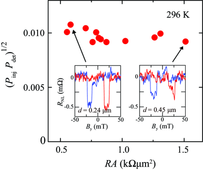
From the results shown in Fig. 2, the spin polarization created in n-Ge can be expected. Figure 3 shows a plot of room-temperature spin polarization, , versus the value in the low bias voltage range ( 1.0 V) for various LSV devices. We cannot see the effect of the value of the used contacts on the spin polarization created in n-Ge. Here, for LSVs with 1 km2, the values were reliably observable, and this range was much lower than that in previous room-temperature works.KAIST ; Jamet We note that the use of our Schottky tunnel barriers with inserted -doped layersGe_Hama3 enables us to simultaneously demonstrate room-temperature spin transport and low spin injection/detection. This technique will open a way to develop Ge spintronic applications with low power consumption. We will comment on this point later. Unfortunately, the spin polarization created in n-Ge is still small, 0.01, as shown in Fig. 3. According to the conventional spin diffusion theory,Fert the ratio of ( ) to is important for obtaining a large the spin signal in an LSV with tunnel barriers, where = . Here, because is estimated to be 8.4 m2 in this study, / is 102, which is not an optimum condition.Fert To enhance the spin signals in our LSVs, it might be important to control the value toward 10 m2 by engineering the ferromagnet/n+-Ge junctions. However, we have to consider the spin absorption effect at the low- interface in future. Although the bulk spin polarization of CFA electrodes is expected to be high,Sukegawa the quality of the CFA electrode near the heterointerface may not be sufficient to achieve device applications. If the bulk spin polarization of the low-temperature grown CFA near the interface is degraded,Lazarov we should improve the spin polarization created in n-Ge by achieving high-quality ordered structures. In the study of GaAs-based LSVs, the spin injection/detection efficiency has reportedly be improved by using high-quality Co-based Heusler alloys.Bruski ; Crowell ; Tezuka ; Uemura_PRBR To obtain even higher spin signals at room temperature in Ge-based LSVs, we should further improve the quality of the Co-based Heusler alloys on Ge.
Finally, we comment on the technical advantage of using Schottky tunnel barriers for Ge spintronic applications. According to our previous works,Hamaya_FLP high-quality Heulser-alloy/Ge heterointerfaces grown by low-temperature MBE can reduce the influence of the strong Fermi level pinning on the Schottky barrier height. For such Heulser-alloy/n-Ge junctions, we can apply a developed P -doping techniqueMYamada to reduce the width of the Schottky barrier. By utilizing both methods for Schottky tunnel junctions, we can realize high-quality Heulser-alloy/Ge contacts with relatively low values ( 1 km2).MYamada ; Ge_Hama3 For ferromagnet/MgO/n-Ge junctions, on the other hand, there are many reports on the use of the barrier layers (1 2 nm) to obtain relatively high values ( 100 km2) in the low bias voltage range ( 1.0 V). In addition, complete Fermi level depinning cannot be observed yet by inserting crystalline MgO barriers between bcc-ferromagnets and n-Ge.Zhou_FLP For these reasons, our Schottky tunnel barriers are more effective than ferromagnet/MgO barriers for simultaneously demonstrating room-temperature spin transport and low contacts in the Ge spintronic devices.
In summary, we reported on room-temperature four-terminal nonlocal spin signals and Hanle-effect curves obtained under parallel and anti-parallel magnetization states of Co2FeAl (CFA) Schottky tunnel contacts in n-Ge-based LSVs. Using the analyses of the Hanle-effect curves and -dependent nonlocal spin signals, we extracted a room temperature Ge value of 0.44 0.02 m for n-Ge ( 1 1019 cm-3). We note that room-temperature spin signals can be observed for LSVs with a relatively low of 1 km2, which is much lower than that of ferromagnet/MgO tunnel contacts obtained in previous room-temperature works.Jamet ; KAIST This study will pave a way to develop Ge spintronic applications with low power consumption.
This work was partially supported by a Grant-in-Aid for Scientific Research (A) (No. 16H02333) from the Japan Society for the Promotion of Science (JSPS), and a Grant-in-Aid for Scientific Research on Innovative Areas ‘Nano Spin Conversion Science’ (No. 26103003) from the Ministry of Education, Culture, Sports, Science and Technology (MEXT). M.Y. acknowledges scholarships from the Toyota Physical and Chemical Research Institute Foundation. Y.F. acknowledges JSPS Research Fellowships for Young Scientists.
References
- (1) I. Žutić, J. Fabian, and S. Das Sarma, Rev. Mod. Phys. 76, 323 (2004).
- (2) S. Yuasa and D. D. Djayaprawira, J. Phys. D 40, R337 (2007).
- (3) M. Tanaka and S. Sugahara, IEEE Trans. Electron Devices 54, 961 (2007).
- (4) T. Taniyama, E. Wada, M. Itoh and M. Yamaguchi, NPG Asia Mater. 3, 65 (2011).
- (5) A. Hirohata and K. Takanashi, J. Phys. D: Appl. Phys. 47, 193001 (2014).
- (6) I. Appelbaum, B. Huang, and D. J. Monsma, Nature (London) 447, 295 (2007); I. Appelbaum, Phil. Trans. R. Soc. A 369, 3554 (2011).
- (7) O. M. J. van’t Erve, A. T. Hanbicki, M. Holub, C. H. Li, C. Awo-Affouda, P. E. Thompson, and B. T. Jonker, Appl. Phys. Lett. 91, 212109 (2007).
- (8) S. P. Dash, S. Sharma, R. S. Patel1, M. P. Jong and R. Jansen, Nature 462, 491 (2009); R. Jansen, Nature Mat. 11, 400 (2012).
- (9) Y. Ando et al., Appl. Phys. Lett. 94, 182105 (2009); Y. Ando et al., Appl. Phys. Exp. 3, 093001 (2010); Y. Ando et al., Appl. Phys. Lett. 99, 132511 (2011); K. Hamaya et al., J. Appl. Phys. 113, 17C501 (2013).
- (10) T. Sasaki, T. Oikawa, T. Suzuki, M. Shiraishi, Y. Suzuki, and K.Tagami, Appl. Phys. Exp. 2, 053003 (2009); T. Suzuki, T. Sasaki, T. Oikawa, M. Shiraishi, Y. Suzuki, and K. Noguchi, Appl. Phys. Exp. 4, 023003 (2011); T. Sasaki, Y. Ando, M. Kameno, T. Tahara, H. Koike, T. Oikawa, T. Suzuki and M. Shiraishi, Phys. Rev. Applied 2, 034005 (2014).
- (11) Y. Saito et al., J. Appl. Phys. 115, 17C514 (2014); Y. Saito et al., J. Appl. Phys. 117, 17C707 (2015); M. Ishikawa et al., Phys. Rev. B 95, 115302 (2017).
- (12) D. Kuzum, A. J. Pethe, T. Krishnamohan, and K. C. Saraswat, IEEE Trans. Electron Devices 56, 648 (2009).
- (13) R. Zhang, T. Iwasaki, N. Taoka, M. Takenaka, and S. Takagi, IEEE Trans. Electron Devices 59, 335 (2012).
- (14) Y. Zhou, W. Han, L.-T. Chang, F. Xiu, M. Wang, M. Oehme, I. A. Fischer, J. Schulze, R. K. Kawakami, and K. L. Wang, Phys. Rev. B 84, 125323 (2011); L.-T. Chang, W. Han, Y. Zhou, J. Tang, I. A. Fischer, M. Oehme, J. Schulze, R. K. Kawakami, and K. L. Wang, Semicond. Sci. Technol. 28, 015018 (2013).
- (15) H. Saito, S. Watanabe, Y. Mineno, S. Sharma, R. Jansen, S. Yuasa, and K. Ando, Solid State Commun. 151, 1159 (2011); A. Spiesser, H. Saito, R. Jansen, S. Yuasa, and K. Ando, Phys. Rev. B 90, 205213 (2014).
- (16) K-R. Jeon, B-C. Min, Y-H. Jo, H-S. Lee, I-J. Shin, C-Y. Park, S-Y. Park, and S-C. Shin, Phys. Rev. B 84, 165315 (2011).
- (17) K. Kasahara et al., J. Appl. Phys. 111, 07C503 (2012); K. Hamaya et al., J. Appl. Phys. 113, 183713 (2013).
- (18) A. Jain et al., Phys. Rev. Lett. 109, 106603 (2012); J.-C. Rojas-Sánchez et al., Phys. Rev. B. 88, 064403 (2013).
- (19) K. Kasahara et al., Appl. Phys. Exp. 7, 033002 (2014); M. Kawano et al., Appl. Phys. Lett. 109, 022406 (2016).
- (20) Y. Fujita et al., Phys. Rev. B 94, 245302 (2016); M. Yamada et al., Phys. Rev. B 95, 161304(R) (2017); Y. Fujita et al., Phys. Rev. Applied 8, 014007 (2017).
- (21) S. Dushenko, M. Koike, Y. Ando, T. Shinjo, M. Myronov, and M. Shiraishi, Phys. Rev. Lett. 114, 196602 (2015).
- (22) M. Johnson and R. H. Silsbee, Phys. Rev. Lett. 55, 1790 (1985).
- (23) F. J. Jedema, H. B. Heersche, A. T. Filip, J. J. A. Baselmans, and B. J. van Wees, Nature 416, 713 (2002).
- (24) T. Kimura and Y. Otani, J. Phys. Condens. Matter 19, 165216 (2007).
- (25) X. Lou, C. Adelmann, S. A. Crooker, E. S. Garlid, J. Zhang, K. S. M. Reddy, S. D. Flexner, C. J. Palmstrøm, and P. A. Crowell, Nat. Phys. 3, 197 (2007).
- (26) K. Sawano, Y. Hoshi, S. Kudo, K. Arimoto, J. Yamanaka, K. Nakagawa, K. Hamaya, M. Miyao, and Y. Shiraki, Thin Solid Films 613, 24 (2016).
- (27) M. Yamada, K. Sawano, M. Uematsu, and K. M. Itoh, Appl. Phys. Lett. 107, 132101 (2015); M. Yamada, Y. Fujita, S. Yamada, T. Kanashima, K. Sawano, and K. Hamaya, Mat. Sci. Semicon. Proc., 2017 (in press); doi: 10.1016/j.mssp.2016.07.025.
- (28) W. Wang, H. Sukegawa, R. Shan, S. Mitani and K. Inomata, Appl. Phys. Lett. 95, 182502 (2009); Z. Wen, H. Sukegawa, S. Kasai, M. Hayashi, S. Mitani and K. Inomata, Appl. Phys. Exp. 5, 063003 (2012).
- (29) S. Yamada et al., Appl. Phys. Lett. 105, 071601 (2014); Tanikawa et al., Thin Solid Films 557, 390 (2014).
- (30) A. Dimoulas, A. Toriumi, and S. E. Mohney, MRS bulletin 34, 522 (2009).
- (31) R. Vrijen, E. Yablonovitch, K. Wang, H. W. Jiang, A. Balandin, V. Roychowdhury, T. Mor, and, D. DiVincenzo, Phys. Rev. A 62, 012306 (2000).
- (32) L. O’Brien, D. Spivak, N. Krueger, T. A. Peterson, M. J. Erickson, B. Bolon, C. C. Geppert, C. Leighton, and P. A. Crowell, Phys. Rev. B 94, 094431 (2016).
- (33) Y. Song, O. Chalaev, and H. Dery, Phys. Rev. Lett. 113, 167201 (2014).
- (34) A. Fert, J.-M. George, H. Jaffrès, and R. Mattana, IEEE Trans. Electron Devices 54, 921 (2007).
- (35) Z. Nedelkoski, B. Kuerbanjiang, S. E. Glover, A. Sanchez, D. Kepaptsoglou, A. Ghasemi, C. W. Burrows, S. Yamada, K. Hamaya, Q. Ramasse, P. Hasnip, T. Hase, G. Bell, A. Hirohata, and V. Lazarov, Sci. Rep. 6, 37282 (2016).
- (36) T. Saito, N. Tezuka, M. Matsuura and S. Sugimoto, Appl. Phys. Express 6, 103006 (2013).
- (37) P. Bruski, S. C. Erwin, J. Herfort, A. Tahraoui, and M. Ramsteiner, Phys. Rev. B 90, 245150 (2014).
- (38) T. Uemura, T. Akiho, Y. Ebina, and M. Yamamoto, Phys. Rev. B 91, 140410(R) (2015).
- (39) T. A. Peterson, S. J. Patel, C. C. Geppert, K. D. Christie, A. Rath, D. Pennachio, M. E. Flatté, P. M. Voyles, C. J. Palmstrøm, and P. A. Crowell, Phys. Rev. B 94, 235309 (2016).
- (40) K. Yamane et al., Appl. Phys. Lett. 96, 162104 (2010); K. Kasahara et al., Phys. Rev. B 84, 205301 (2011); K. Kasahara et al., Appl. Phys. Lett. 104, 172109 (2014).
- (41) Y. Zhou, W. Han, Y. Wang, F. Xiu, J. Zou, R. K. Kawakami, and K. L. Wang, Appl. Phys. Lett. 96, 102103 (2010).