Correspondence and requests should be addressed to S.F.F.] (e-mail: sfischer@physik.hu-berlin.de).
High-temperature quantum oscillations of the Hall resistance in bulk Bi2Se3
Helically spin-polarized Dirac fermions (HSDF) in protected topological surface states (TSS) are of high interest as a new state of quantum matter. In three-dimensional (3D) materials with TSS, electronic bulk states often mask the transport properties of HSDF. Recently, the high-field Hall resistance and low-field magnetoresistance indicate that the TSS may coexist with a layered two-dimensional electronic system (2DES). Here, we demonstrate quantum oscillations of the Hall resistance at temperatures up to 50 K in bulk Bi2Se3 with a high electron density of about cm-3. From the angular and temperature dependence of the Hall resistance and the Shubnikov-de Haas oscillations we identify 3D and 2D contributions to transport. Angular resolved photoemission spectroscopy proves the existence of TSS. We present a model for Bi2Se3 and suggest that the coexistence of TSS and 2D layered transport stabilizes the quantum oscillations of the Hall resistance.
Among the new material class of topological insulators (TI), the chalcogenide semiconductor Bi2Se3 has been long subject to intense investigations due to its potential integration in room temperature applications, such as dissipationless electronics and spintronics devices1; 2; 4; 3. Bi2Se3 has a single Dirac cone at the -point in the first surface Brillouin zone and a direct band gap of 0.3 eV between the valence and the conduction band5; 6; 7. Due to the inversion symmetry in Bi2Se3 the topological invariant is equal to the charge of parity of the valence band eigenvalues at the time-reversal-invariant points of the first Brillouin zone caused by the band inversion8. In the crystalline modification Bi2Se3 has a tetradymite structure with Rm symmetry. The unit cell consists of 15 atomic layers grouped in three quintuple layers (QLs) with SeBiSeBiSe order stacked in an ABCABC manner. The quintuple layers are van der Waals bonded to each other by a double layer of Se atoms, the so-called van der Waals gap4. The existence of TSS in Bi2Se3 has been experimentally confirmed through angle resolved photoemission spectroscopy (ARPES)7; 9; 3 and scanning tunneling microscopy/scanning tunneling spectroscopy (STM/STS)10; 11. The as-grown crystals of Bi2Se3 are typically -type because of electron doping due to natural selenium vacancies12; 13. Therefore, the transport properties of Bi2Se3 are generally dominated by bulk conduction. In particular, the temperature dependence of the electrical resistivity is metallic-like3; 17; 14; 15; 16 and Shubnikov-de Haas (SdH) oscillations in the longitudinal resistivity show the characteristic signatures for a 3D Fermi surface17; 14. For samples with lower carrier density cm-3, the TSS can be detected via additional SdH oscillations with a frequency higher than that of the bulk18. The Hall resistivity exhibits quantum oscillations for a carrier density cm-3. Recently, for cm-3 a bulk quantum Hall effect (QHE) with 2D-like transport behavior was reported3; 14; 16. Its origin remains unidentified.
In this work we demonstrate that the quantum oscillations of the Hall resistance in high-purity, nominally undoped Bi2Se3 single crystals with a carrier density of cm-3 persists up to high temperatures. The longitudinal resistivity and the Hall resistivity were measured simultaneously in a temperature range between 0.3 K and 72 K in tilted magnetic fields up to 33 T. The SdH oscillations in are clearly dominated by 3D bulk carriers. The quantum oscillations of the Hall resistance scales with the sample thickness, strongly indicating 2D layered transport. These findings stand out because the Bi2Se3 sample investigated here has a lower carrier mobility of about cm2/(Vs) than materials hosting a typical 2D Fermi gas19; 20; 21; 22 or 3D Fermi gas23; 24; 25 showing QHE. We discuss the conditions of the QHE below in detail and present a model for the coexistence of TSS and 2D layered transport.
Results
Experimental data. In Fig. 1a, we show high-reso- lution ARPES dispersions measured at a temperature of 12 K for two representative photon energies of h eV and 21 eV. We clearly observe distinct intensity contributions from the bulk conduction band (BCB) and bulk valence band (BVB) coexisting with sharp and intense Dirac cone representing the TSS. The BCB crossing the Fermi level indicates that the crystals are intrinsically -type, in agreement with our Hall measurements on the same samples. At binding energies higher than the Dirac node ( eV), the lower half of the TSS overlaps with the BVB. By changing the photon energy we select the component of the electron wave vector perpendicular to the surface . Since the lattice constant of Bi2Se3 is very large along the direction ( Å), the size of the bulk Brillouin zone (BBZ) is very small ( Å-1). With photon energies between 16 to 21 eV we cross practically the complete BBZ, enhancing the sensitivity to the out-of-plane dispersion of the bulk bands. We note that the ARPES intensity changes with the photon energy as well due to the -dependence of the photoemission transitions. Differently from the BCB or BVB, the TSS exhibits no -dependence due to its 2D character. Consistent with the direct nature of the gap, we find the BCB minimum at 21 eV (-point of the BBZ) and at a binding energy of eV, while the BVB maximum at eV. In particular, from the ARPES measurements, we
estimate a bulk carrier density of cm-3 and a sheet carrier density of cm-2, with Å-1 and Å-1, respectively.
The temperature-dependent longitudinal resistance at zero magnetic field shows metallic-like behavior (see inset of Fig. 1c). A residual resistance ratio indicates a high crystalline quality12 (see Supplementary Information Sec. 1). The resistance remains practically constant from very low temperatures up to 30 K, presumably due to a combination of surface states and static disorder scattering of the charge carriers. These observations are in agreement with previous reports3; 14; 16; 15; 26; 27.
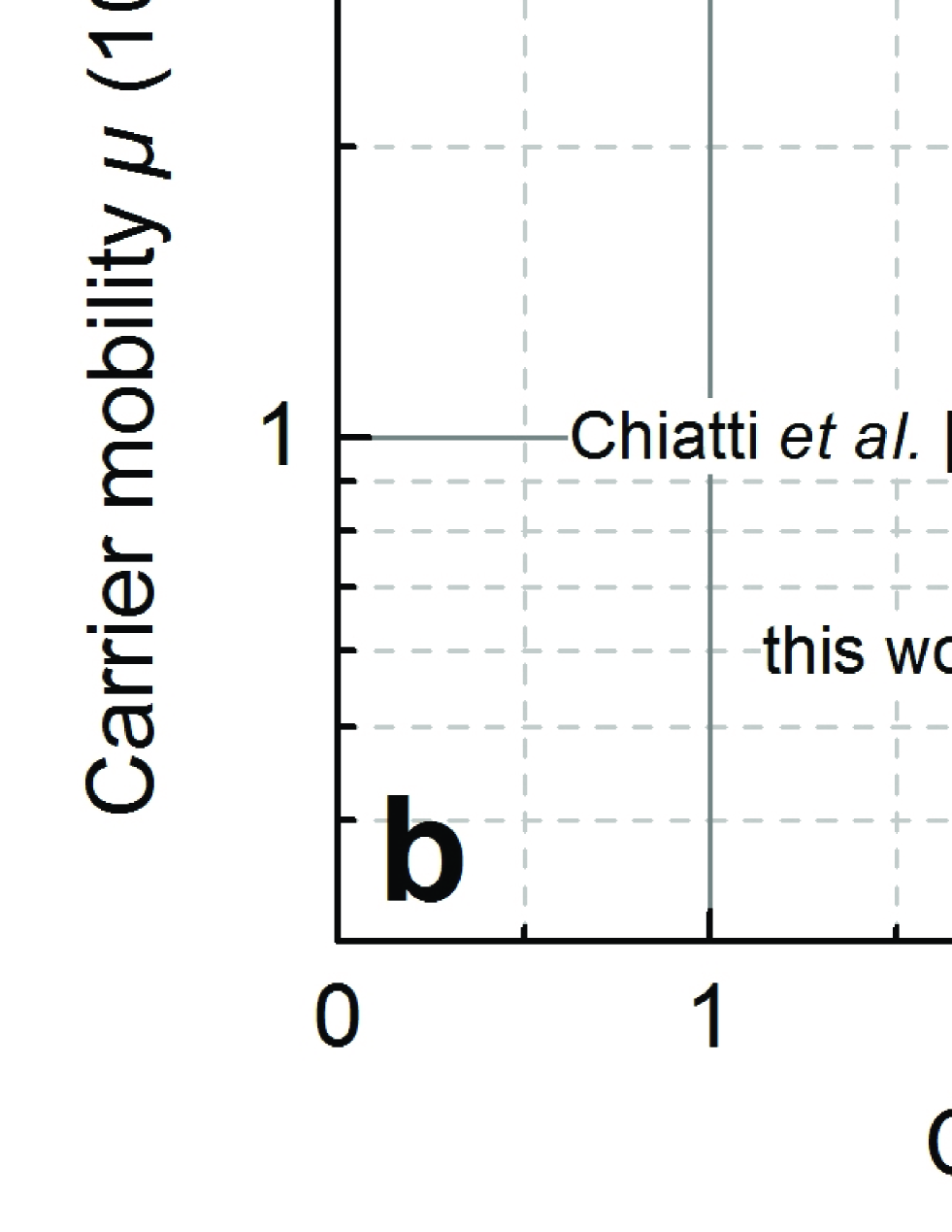
SdH oscillations in the longitudinal resistivity and the onset of quantum oscillations of the Hall resistivity can be observed at magnetic fields T. Fig. 1d depicts (blue curve, left axis) and (red curve, right axis) as a function of the perpendicular magnetic field at a temperature of K. In Fig. 1c we show the corresponding longitudinal resistance vs perpendicular magnetic field measured at K as symmetrized raw data . The slope of the Hall resistivity yields a carrier mobility of cm2/(Vs) and a carrier density of cm-3. In Fig. 1b we compare the carrier mobility vs carrier density of various crystalline Bi2Se3 samples, obtained in magnetotransport measurements. Our data are in the medium carrier density and mobility range.
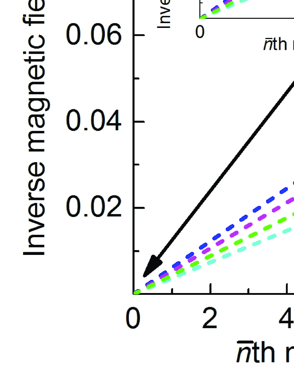
Fig. 2a details the analysis performed on the high-field anti-symmetrized data for K and an angle of . denotes the angle between the direction of and the surface normal and the -axis of the Bi2Se3 macro flake (i.e. means ). The scaling behaviour of with the thickness leads to as the number of 2D spin-degenerate layers contributing to the transport. Conclusively, an average number of 2D layers of is derived. The variation of for different Landau level (LL) index is given in inset of Fig. 2a.
Figs. 2c and 2d depict the angular and the temperature dependence, respectively, of the negative differentiated Hall resistivity vs magnetic field , determined for different angles at K, as well as different temperatures for . In accordance with the angular and the temperature dependence of the SdH oscillations as shown in Figs. 3a and 4a, respectively, a decreasing amplitude of the differentiated Hall resistivity with increasing angle and increasing temperature is detected. At a constant temperature of K the typical signatures of quantum oscillations of the Hall resistance are observed up to an angle of and at the amplitude of vanishes only for temperatures above 71.5 K.
In the LL fan diagram shown in Fig. 2b the inverse magnetic-field positions are plotted vs the th minimum of the longitudinal resistivity for different values of . The straight dashed lines, which represent the best linear fits to the data, intersect jointly the -axis at the point of origin (see Supplementary Information Sec. 2). Hence, we find for all angles and temperatures investigated here a significant evidence for a trivial Berry phase of (cf. inset of Fig. 2b) and conclude the dominance of non-relativistic fermions. For an improved estimation of the trivial Berry phase we have fitted the behavior of the relative longitudinal resistivity vs magnetic field assuming 2D and 3D transport (cf. Fig. 4c and d, respectively).
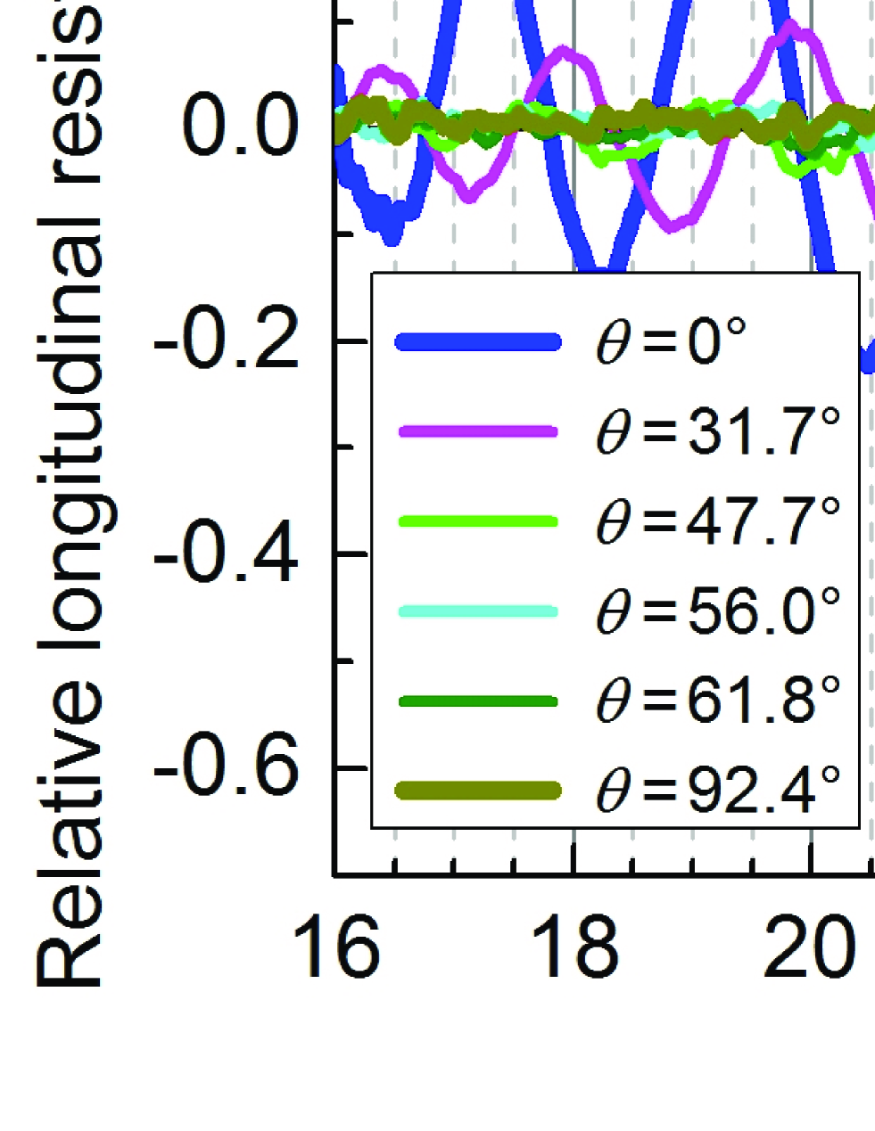
In Fig. 3a we show the relative longitudinal resistivity vs magnetic field measured at K for different angles . The relative longitudinal resistivity was calculated from the measured longitudinal resistivity by subtracting a suitable polynominal fit to the background, in order to extract the oscillatory component. The amplitude of the SdH oscillations decreases with increasing angle , and is really marginal for . Furthermore, a shift of the SdH oscillations with increasing angle with respect to is observed. For all values of and , we found one value of the SdH frequency . The absence of additional frequencies and beatings, as well as the angular dependence of (see Fig. 3b), are significant evidence of a single 3D (non-spherical) Fermi surface (see Supplementary Information Sec. 3).
The temperature dependence of is shown in Fig. 4a: the amplitude decreases with increasing temperature , and oscillations are not observed for K. From the fitting of the relative longitudinal resistivity ratio K), we deduce an effective mass of the charge carriers of ( kg denotes the electron rest mass) and a Fermi velocity of m/s, with Å-1.
The Dingle plots (inset of Fig. 4b) at temperatures of K, 4.22 K, 15.3 K, and 26 K yield the following Dingle scattering time (also known as single-particle relaxation time) and the Dingle temperature , assuming the fit function with : s ( K), s (23.7 K), s (30.9 K) and s (45.5 K), respectively.
For a more detailed analysis we have fitted the magnetic-field dependence of (see Supplementary Information Sec. 4). In a first step we assumed 2D transport in accordance with other investigations14; 15; 26 and have used as fit function the Lifshitz-Kosevich formula4; 28; 29. Although we found a reasonably good agreement between experimental data and the calculated behavior for under the assumption of 2D transport (cf. Fig. 4c), we also performed fits under the assumption of 3D transport (cf. Fig. 4d). This is motivated by the analysis of the angular dependence of the SdH frequency shown in Fig. 3b, were we found an ellipsoidal 3D Fermi surface. We find for all curves a single value for the Dingle temperature K and hence a single value for the Dingle scattering time s, consistent with a constant up to K (see inset of Fig. 1c). From and the effective mass , we determined a carrier mobility of cm2/(Vs).
Evaluation of experimental data. The angle dependence of the SdH oscillations was used to determine the ellipsoidal shape of the Fermi surface. For a plane 2D Fermi surface, the SdH oscillation frequency is equal to , with for (blue curve in Fig. 3b) and for an ellipsoidal 3D Fermi surface it is (red curve in Fig. 3b), with T and T. Previous data15; 16 may also be interpreted as 3D ellipsoidal Fermi surface (see Supplementary Information Sec. 3).
We estimate the ellipsoidal cross-section of the 3D Fermi surface with the wave vectors Å-1 and Å-1. With these values we deduced an eccentricity for the 3D non-spherical Fermi surface of . Köhler30 and Hyde et al.12 show, that the eccentricity of the non-spherical Fermi surface decreases with decreasing carrier density . In accordance with the present study, Eto et al.14 deduced for a Bi2Se3 bulk single crystal with a lower carrier density of cm-3 an eccentricity of , consistent with eccentricities obtained by Köhler30. Assuming a parabolic dispersion and using the values of and from the SdH analysis and of from the ARPES measurements, we estimate with for the effective masses and . An average value for the effective mass is then given by31 , which yields . This value is consistent with the value obtained from the temperature dependence of the SdH oscillations: .
Discussion
Generally, a bulk or 3D QHE is attributed to parallel 2D conduction channels, each made from one or a few stacking layers. A bulk QHE, where quantized values of the Hall resistance inversely scale with the sample thickness, has been observed in a number of anisotropic, layered electronic bulk materials, e.g., GaAs/AlGaAs multi-quantum wells20, Bechgaard salts24; 33 and also in Fe-doped Bi2Se3 bulk samples34, where transport by TSS was excluded. However, the observation of the quantum oscillations of the Hall resistance in Bi2Se3 at elevated temperatures calls for a special condition considering the usual requirement of . In the present case T and the carrier mobility cm2/(Vs) yields only . Furthermore, the deduced effective mass yields for a magnetic field of T, where we observe the onset of the quantum oscillations of the Hall resistance , a value for the LL energy splitting of meV. However, the thermal energy amounts to meV at K, while is usually required for a QHE. Nevertheless, we observe unambiguous signatures of quantum oscillations in , as shown in Figs. 2c and 2d.
In order to explain the experimental observations, we propose the following model. The Bi2Se3 bulk sample investigated here may consist of three different conducting regions: a semiconducting-like core region, surrounded by a metallic-like shell region and the topological surface (see Fig. S1 in Supplementary Information Sec. 5). The semiconducting-like core was proven by the preparation of semiconducting micro flakes3. The metallic-like shell region due to Se depletion dominates the transport mechanism observed here as metallic and 2D layered effects. From our experiments, we assume the shell to form a stacked system of 2D layers with a periodic potential23 either due to the van der Waals-gaps or the unit cell along the -axis because of the carrier density modulation due to Se vacancies. In magnetic fields the thickness scaling of the plateaux-like features in the Hall resistance yields an effective thickness for the shell of stacked 2D layers. For the charge carrier density, we estimate three different values for the core3, the shell and the topological surface: cm-3, cm-3 and cm-2, respectively. In the semiconducting-like core region, the Fermi level (chemical potential) is in the gap close to the bottom of the conduction band, whereas in the metallic-like shell region the Fermi level is in the conduction band (see Supplementary Information Sec. 5).
For the SdH frequency we estimate at for the three regions the following values: T, T and T. The small value corresponds to a slow-changing background which is out of the measurement range of our experimental setup. The larger value of the TSS is caused only by the small number of surface electrons with respect to the large number of bulk electrons ( and yield a ratio ). Therefore, from the experimental data we deduce only the value for the shell (see Fig. 3a) and find the dominant contribution of the bulk (core+shell) in the transport behavior. A periodic modulation of the charge carrier density along the -direction would result in a miniband structure for the LLs and, as long as the Fermi level is in a gap between these minibands, the Hall resistivity will be quantized and scale with the periodicity of the potential23. The persistence of the quantum oscillations of the Hall resistance up to high temperatures requires the Fermi level pinning in the miniband gap. Therefore, we conclude that the observation of the quantum oscillations of the Hall resistance at higher temperatures in Bi2Se3 with a majority of non-Dirac Fermions is related to the existence of the TSS. Based on our results, we propose that other 3D materials with TSS and a periodic potential modulation may show quantization effects in the Hall resistance at elevated temperatures.
Methods
High-quality single crystalline Bi2Se3 was prepared from melt with the Bridgman technique. The growth time, including cooling was about 2 weeks for a 50 g crystal. The whole crystal was easily cleaved along the [00.1] growth direction, indicating crystal perfection. The macro flake was prepared by cleaving the bulk single crystal with a thickness of around 110 m to investigate bulk properties.
We explored the structural properties of the bulk single crystal3 with atomic force microscopy (AFM), scanning transmission electron microscopy (STEM) and high-resolution transmission electron microscopy (HRTEM). The composition and surface stability were investigated using energy-dispersive x-ray spectroscopy (EDX) and spatially resolved core-level X-ray PEEM. Structural analysis using HRTEM and STEM was carried out at a JEOL JEM2200FS microscope operated at 200 kV. The sample preparation for HRTEM characterization consisted of ultrasonic separation of the flakes from the substrate, followed by their transfer onto a carbon-coated copper grid. Using adhesive tape, the surface was prepared by cleavage of the crystal along its trigonal axis in the direction perpendicular to the van-der-Waals-type planes. The ARPES measurements were performed at a temperature of 12 K in an ultra-high vacuum (UHV) chamber at a pressure of mbar with a VG Scienta R8000 electron analyzer at the UE112-PGM2a beamline of BESSY II using p-polarized undulator radiation.
We have performed magnetotransport experiments using a standard low-noise Lock-In techniques (Stanford Research Systems SR830 with a Keithley 6221 as current source), with low excitation to prevent heating of the sample. The Bi2Se3 macro flake has been measured in a flow cryostat (1.3 K to 300 K), as well as in a 3He insert (down to 0.3 K), in a Bitter magnet with a bore diameter of 32 mm and with magnetic fields up to 33 T at the High Field Magnet Laboratory (HFML) of the Radboud University Nijmegen. In both setups, we used a Cernox thermometer in the vicinity of the sample to monitor the temperature in situ. In the 3He system, the temperature between 0.3 K and 1.3 K was stabilized by the 3He vapour pressure prior to the magnetic field sweep to assure a constant temperature. However, the temperature between 1.3 K and 4.2 K was stabilized by the 4He pressure. Above a temperature of 4.2 K, we have used the flow cryostat and stabilized the temperature using a capacitance.
References
- (1) Xue, Q.-K. Nanoelectronics: A topological twist for transistors. Nature Nanotechnol. 6, 197 (2011).
- (2) Zhang, H. et al. Topological insulators in Bi2Se3, Bi2Te3 and Sb2Te3 with a single Dirac cone on the surface. Nature Phys. 5, 438 (2009).
- (3) Chiatti, O. et al. 2D layered transport properties from topological insulator Bi2Se3 single crystals and micro flakes. Sci. Rep. 6, 27483 (2016).
- (4) Ando, Y. Topological Insulator Materials. J. Phys. Soc. J. 82, 102001 (2013).
- (5) Checkelsky, J. G., Hor, Y. S., Cava, R. J. Ong, N. P. Bulk band gap and surface state conduction observed in voltage-tuned crystals of the topological insulator Bi2Se3. Phys. Rev. Lett. 106, 196801 (2011).
- (6) Betancourt, J. Li, S., Dang, X., Burton, J. D., Tsymbal, E. Y. Velev, J. P. Complex band structure of topological insulator Bi2Se3. J. Phys.: Condens. Matter 28, 395501 (2016).
- (7) Xia, Y. et al. Observation of a large-gap topological-insulator class with a single Dirac cone on the surface. Nature Phys. 5, 398 (2009).
- (8) Fu, L. Kane, C. L. Topological insulators with inversion symmetry. Phys. Rev. B 76, 045302 (2007).
- (9) Bianchi, M. et al. The electronic structure of clean and adsorbate-covered Bi2Se3: an angle-resolved photoemission study. Semicond. Sci. Technol. 27, 124001 (2012).
- (10) Alpichshev, Z. et al. STM Imaging of Impurity Resonances on Bi2Se3. Phys. Rev. Lett. 108, 206402 (2012).
- (11) Liu, Y. et al. Tuning Dirac states by strain in the topological insulator Bi2Se3. Nature Phys. 10, 294 (2014).
- (12) Hyde, G. R., Beale, H. A., Spain, I. L. Woollam, J. A. Electronic properties of Bi2Se3 crystals. J. Phys. Chem. Solids 35, 1719 (1974).
- (13) Yan, B., Zhang, D. Felser, C. Topological surface states of Bi2Se3 coexisting with Se vacancies. Phys. Status Solidi RRL 7, 148 (2013).
- (14) Eto, K. Ren, Z., Taskin, A. A., Segawa, K. Ando Y. Angular-dependent oscillations of the magnetoresistance in Bi2Se3 due to the three-dimensional bulk Fermi surface. Phys. Rev. B 81, 195309 (2010).
- (15) Petrushevsky, M. et al. Probing the surface states in Bi2Se3 using the Shubnikov-de Haas effect. Phys. Rev. B 86, 045131 (2012).
- (16) Cao, H. et al. Quantized Hall Effect and Shubnikov-de Haas Oscillations in Highly Doped Bi2Se3: Evidence for Layered Transport of Bulk Carriers. Phys. Rev. Lett. 108, 216803 (2012).
- (17) Analytis, J. G. et al. Bulk Fermi surface coexistence with Dirac surface state in Bi2Se3: A comparison of photoemission and Shubnikov-de Haas measurements. Phys. Rev. B 81, 205407 (2010).
- (18) Analytis, J. G. et al. Two-dimensional surface state in the quantum limit of a topological insulator. Nature Phys. 6, 960 (2010).
- (19) Beenakker, C. W. J. van Houten, H. Quantum transport in semiconductor nanostructures. Sol. St. Phys. 44, 1 (1991).
- (20) Störmer, H. L., Eisenstein, J. P., Gossard, A. C., Wiegmann, W. Baldwin, K. Quantization of the Hall effect in an anisotropic three-dimensional electronic system. Phys. Rev. Lett. 56, 85 (1986).
- (21) Novoselov, K. S. et al. Room-Temperature Quantum Hall Effect in Graphene. Science 315, 1379 (2007).
- (22) Khouri, T. et al. High-temperature quantum Hall effect in finite gapped HgTe quantum wells. Phys. Rev. B 93, 125308 (2016).
- (23) Halperin, B. I. Possible States for a Three-Dimensional Electron Gas in a Strong Magnetic Field. Jap. J. Appl. Phys. 26, 1913 (1987).
- (24) Hannahs, S. T., Brooks, J. S., Kang, W., Chiang, L. Y. Chaikin, P. M. Quantum Hall effect in a bulk crystal. Phys. Rev. Lett. 63, 1988 (1989).
- (25) Hill, S. et al. Bulk quantum Hall effect in -Mo4O11. Phys. Rev. B 58, 10778 (1998).
- (26) Yan, Y. et al. High-Mobility Bi2Se3 Nanoplates Manifesting Quantum Oscillations of Surface States in the Sidewalls. Sci. Rep. 4, 3817 (2014).
- (27) Liu, H., Liu, S., Yi, Y., He, H. Wang, J. Shubnikov de Haas oscillations in and type Bi2Se3 flakes. 2D Materials 2, 045002 (2015).
- (28) Lifshitz, E. M. Pitaevskii, L. P. Statistical Physics. Pergamon Press, Oxford (1986).
- (29) Taskin, A. A. Ando, Y. Berry phase of nonideal Dirac fermions in topological insulators. Phys. Rev. B 84, 035301 (2011).
- (30) Köhler, H. Conduction Band Parameters of Bi2Se3 from Shubnikov-de Haas Investigations. Phys. Stat. Sol. (b) 58, 91 (1973).
- (31) Ziman, J. M. Electrons and Phonons The Theory of Transport Phenomena in Solids. Clarendon Press, Oxford (2001).
- (32) Landwehr, G. et al. Quantum transport in n-type and p-type modulation-doped mercury telluride quantum wells. Physica E 6, 713 (2000).
- (33) Balicas, L., Kriza, G. Williams, F. I. B. Sign Reversal of the Quantum Hall Number in (TMTSF)2PF6. Phys. Rev. Lett. 75, 2000 (1995).
- (34) Ge, J. et al. Evidence of layered transport of bulk carriers in Fe-doped Bi2Se3 topological insulators. Sol. State Commun. 211, 29 (2015).
Acknowledgements
Financial support from the Deutsche Forschungsgemeinschaft within the priority program SPP1666 (Grant No. FI932/7-1 and RA1041/7-1) and the Bundesministerium für Bildung und Forschung (Grant No. 05K10WMA) is gratefully acknowledged.
Author contributions
M.B., O.C., S.P., S.W. and S.F.F. contributed to the transport experiments, analyzed the data and wrote the manuscript, J.S.-B. and O.R. conducted the ARPES experiments and L.V.Y. conducted the bulk crystal growth. All authors contributed to the discussion and reviewed the manuscript.
Additional information
Supplementary Information is available in the online version of the paper. Reprints and permissions information is available online at www.nature.com/reprints. Correspondence and requests for materials should be addressed to S.F.F.
Competing financial interests
The authors declare no competing financial interests.