Measurements of a Quantum Dot with an Impedance-Matching On-Chip LC Resonator at GHz Frequencies
Abstract
We report the realization of a bonded-bridge on-chip superconducting coil and its use in impedance-matching a highly ohmic quantum dot (QD) to a 3 GHz measurement setup. The coil, modeled as a lumped-element resonator, is more compact and has a wider bandwidth than resonators based on coplanar transmission lines (e.g. impedance transformers and stub tuners) at potentially better signal-to-noise ratios. In particular for measurements of radiation emitted by the device, such as shot noise, the 50 larger bandwidth reduces the time to acquire the spectral density. The resonance frequency, close to 3.25 GHz, is three times higher than that of the one previously reported wire-bonded coil. As a proof of principle, we fabricated an circuit that achieves impedance-matching to a load and validate it with a load defined by a carbon nanotube QD of which we measure the shot noise in the Coulomb blockade regime.
I Introduction
Superconducting qubit control and readout of very resistive quantum devices need microwave (MW) resonators operating at frequencies in the range of GHz. To efficiently measure radiation emitted from a device, one attempts to balance the high device impedance to the characteristic impedance of the usual coaxial lines using an impedance-matching circuit. These circuits are often implemented with superconducting on-chip transmission lines. Examples include quarter-wavelength step transformer in the fluxonium qubit Manucharyan et al. (2009), stub tuners for quantum point contacts Puebla-Hellmann and Wallraff (2012) and QDs Ranjan et al. (2015); Hasler et al. (2015). An alternative approach makes use of an resonator built either from a lumped element inductor Schoelkopf et al. (1998) or form on-chip coils Chen and Liou (2004). However, the resonance frequencies have typically been limited to a maximum of GHz Yue (1998); Xue et al. (2007); Fong and Schwab (2012). It is however important to improve circuits, since they are much less demanding in chip footprint as compared to transmission line circuits. While a transmission line circuit at GHz needs up to cm in length, an appropriate on-chip coil can be fabricated on a smaller area. This is an important consideration for the future scaling of qubit networks for quantum processors. To understand the challenge, the key parameters of an matching circuit are its resonance frequency given by and its characteristic impedance defined as . In order to match to a high-impedance load, should be as large as possible, meaning that one has to aim for a large inductance. At the same time, the resonance frequency should stay high, constraining the capacitance to as small as possible values. In fact, the limiting factor in achievable resonance frequency is the residual stray capacitance in the circuit, which we minimize in our approach.
Addressing the compactness of MW resonators in this work, we fabricated a 200-m-wide on-chip superconducting coil with a wire-bonded bridge (Fig. 1) and utilize it as a lumped matching circuit in a carbon nanotube (CNT) QD noise experiment at a working frequency close to 3.25 GHz. Compared to the one previously reported case of on-chip inductor with bonded bridge Xue et al. (2007); Xue (2010), we achieved a threefold frequency increase with a similar footprint. Comparable compactness has been achieved only with Josephson junction arrays acting as quarter-wavelength resonators Altimiras et al. (2013); Stockklauser et al. (2017).
II Sample fabrication
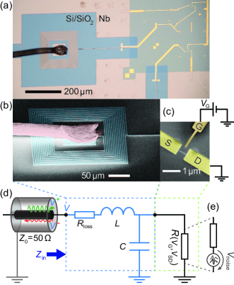
A planar spiral inductor raises the issue of connecting its inner end to the rest of the circuit. While it is possible to fabricate this bridge by lithography, we have realized that the close proximity of the bridge to the coil adds substantial capacitance, limiting the performance of the circuit. In addition, the microfabrication of air-bridges of this kind add several fabrication steps. That is why we developed a solution of bonding a wire between a geometry-restricted inner pad and an external bigger pad at the low-impedance end.
The fabrication starts with preparing a region on the undoped Si / SiO2 (500 m / 170 nm) substrate where CNTs will be placed. Thus, we first evaporate Ti / Au (10 nm / 30 nm) for markers and CNT partial contacts in a square area (top-right corner in Fig. 1(a)). We then protect it with a PMMA/HSQ bilayer resist. Afterwards, we sputter 100 nm of Nb and lift the protection bilayer resist off. Subsequently, we e-beam-pattern bonding pads and the desired inductor in a new PMMA resist layer, then etch the Nb film with an inductively coupled plasma; the surrounding Nb becomes the ground plane. Next, we stamp CNTs Hasler et al. (2015); Viennot et al. (2014) in the predefined region, locate them using a scanning electron microscope (SEM), and contact the chosen CNT in one Ti/Au evaporation step to the coil and to ground (Fig. 1(a)), utilizing the partial contacts. In the same lithography step, a side gate is created at a distance of nm from the CNT (Fig. 1(c)). With the device glued onto a sample holder, we use Al wire to bond the remaining end of the coil to a neighboring bigger pad. Due to the relatively small size of the inner pad (, barely larger than the bonder wedge), the bonding operation is delicate (Fig 1(b)). Finally, we connect the latter pad to the MW line of the printed circuit board sample holder. Furthermore, the Nb ground plane of the sample is bonded with multiple wires along the wafer edge to the sample holder ground plane.
The square spiral inductor used in this experiment (Fig. 1(a,b)) has an outer dimension of 210 m, 14 turns with width and spacing . In the device investigated here two of the turns are shorted, lowering the effective inductance and thus shifting up the resonance frequency by several percents.
III High-frequency setup and resonator characterization
The simplified schematic of the MW circuit is illustrated in Fig. 1(d). The impedance-matching circuit, contained in the light-blue dashed rectangle, is modeled with lumped elements: is the inductance of the coil, its capacitance to ground, and the effective loss resistance, accounting for the RF (radio frequency) loss of the superconducting material and the dielectric loss in the substrate. The input impedance (Fig. 1(d)) reads:
| (1) |
with , the load conductance. can be approximated at by
| (2) |
This approximation is valid for . Full matching is achieved at when . Thus one obtains the condition , meaning that the characteristic impedance of the circuit should be equal to the geometric mean of and , if we neglect . Typical values for are between one and a few k.
In reflectance measurements, a continuous sinusoidal wave is applied to the circuit where it appears with amplitude . Part of the incident signal is reflected back with amplitude due to impedance mismatch. The reflection coefficient is given by:
| (3) |
The magnitude squared of the reflection coefficient is also referred as the reflectance.
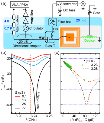
The complete measurement setup, depicted in Fig. 2(a), is the same as in Ref. Hasler et al. (2015). The load of the matching circuit, the CNT device is tuned by and —the DC source-drain and gate voltage, respectively. MW lines are used either in reflectometry mode (a microwave signal is sent to the sample and a reflected signal is read from it) or in noise mode where the MW output line conveys the noise signal produced by the sample. The two respective modes utilize a vector network analyzer (VNA) and a power spectrum analyzer (PSA).
We characterize the impedance-matching resonator by analyzing reflectance measurements together with the simultaneously measured DC current from which we derive the differential conductance . The parameters we thus obtain allow us to extract the QD noise from the measured noise power, as we will show.
In practice, the measured reflection coefficient is not measured at the sample, but rather at the VNA, yielding , where o and i refer to the VNA ports (see Fig. 2(a)). is different from by a frequency-dependent baseline produced by attenuations and amplifications in the setup:
| (4) |
If spurious reflections occur in components across the output line, then standing waves reside in sections of it and the baseline can exhibit a complicated pattern.
In principle, we need to extract 5 parameters, , , , , and . There are two possible approaches: one can fit the frequency dependence of for a fixed known value of , for example for , which is realized when the QD is deep in Coulomb blockade where the current is almost completely suppressed. Fig. 2(b) shows three measured curves for different values. Unfortunately, the baseline function is also markedly frequency-dependent, shifting the minimum of the curves to different values. Due to this dependence, it is already difficult to extract the resonance frequency accurately.
We therefore proceed with the second approach. We fix the frequency to a value close to resonance, in the following to . We carry out simultaneous measurements of reflectance and DC current over several Coulomb diamonds. We obtain the reflectance and the low-frequency maps. For each pair of this defines one point in the - versus - scatter plot. To obtain the circuit parameters, we fit to this scatter plot the theoretical dependence , thereby implicitly assuming that . We have shown in previous work that the real part of the CNT admittance at similar GHz frequencies is the same as Ranjan et al. (2015); Hasler et al. (2015). The curve can be calculated using Eqs. (1,3,4). It is displayed in Fig. 2(c) for a wide range of values. At the resonance frequency, when sweeping the conductance domain from small to large values, first decreases to reach zero reflectance at the matching point where , then increases back for . The fit together with the measured scatter plot is shown in Fig. 2(c).
IV Noise measurement calibration
The current noise produced by a QD can be modeled by a noise voltage source as shown in Fig. 1(d,e). The power spectral density of the voltage source is related to current spectral density by . The noise voltage needs to be transmitted through the circuit to be fed into the - transmission line. The voltage that appears at the interface is proportional to , but contains in addition a frequency-dependent transmission function , which can readily be derived from the circuit parameters:
| (5) |
where and the characteristic impedance as introduced before. In this equation, the factor of shows that the total -factor has three terms, which can be grouped in an internal and an external loss part . The two parts are respectively and . At optimal impedance matching in the lossless picture, i.e. if the condition is met, the external -factor is minimal and given by which yields values around .
The transmitted voltage passes several elements, a directional coupler, a circulator and amplifiers at low and room temperature before being measured with the PSA. The overall gain along the chain is captured by . It was determined with the method presented in Ref. sup to be dB. In addition to the noise generated by the device, the amplifier does also add further current-independent noise. We split the total noise into two contributions and , where the first term describes the noise power which is current-dependent and the second term contains all the rest, i.e. thermal and amplifier noise background. The different terms are related as follows Hasler et al. (2015):
| (6) |
where refers to the excess current noise only (i.e. the thermal noise of the device is included in ).
V Experiment
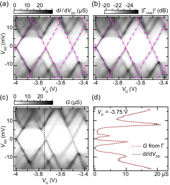
By means of gate and bias voltage sweeps we measure the DC current and draw an initial charge stability diagram. Then we switch to MW reflectance measurements, where we restrict ourselves to a gate span covering a few Coulomb charge states. In this measurement mode, we simultaneously acquire the current and reflectance as functions of and . The VNA was set to the working frequency with an output power of , attenuated by before reaching the device. We deduce the parameters of the impedance-matching circuit from a comparison of the two measured maps (Fig. 3(a)) and (Fig. 3(b)) as described in the previous section. In practice, the conductance domain of the resulted scatter plot does not include values close to , therefore we enrich the plot with a close-to-match point, , from the separately obtained near-match curve in Fig. 2(b).
From complementary measurements we estimate an upper bound of (see Supplemental material). Since , the matching circuit can be modeled as a lossless circuit for practical purposes. Thus we fix , and fit the curve (Fig. 2(c)), which yields nH, fF. We further deduce the resonance frequency and the characteristic impedance ; the resulting match conductance is the minimum of the calculated curve : . For comparison, refitting with , the calculated , , vary by less than 1 %. Furthermore, for we obtain and , yielding an empirical bandwidth .
Consequently, having fixed the parameters we then calculate a full map of the real part of the device admittance, i.e. (Fig. 3(c)). A comparison of cuts (Fig. 3(d)) demonstrates a very good agreement with , confirming the validity of the extracted parameters, at least at the frequency at which the reflectance map was acquired. The advantage of the reflectance measurement is, that can be measured much faster and with less noise, once the circuit parameters are known.
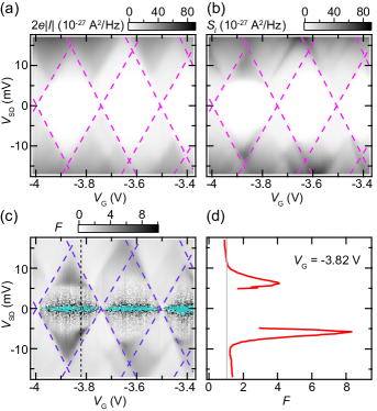
In the noise part of the experiment, we realize simultaneous current and noise measurements over the same few Coulomb diamond span as before. Each retained noise power value arises from averaging 500 identical-input measurements in a bandwidth and it is produced every 800 ms. Fig. 4(b) shows the current noise measured in the same gate range after applying Eq. 6 for calibration. To compare with the Schottky noise, we show in Fig. 4(a) a calculated plot of , where represents the measured DC current. The Fano factor, , is shown in Fig. 4(c). We observe values largely exceeding 1 within the Coulomb blockade, where sequential tunneling of single electrons is forbidden. It is seen in Fig. 4(d) that the Fano factor peaks at mV, where inelastic cotunneling sets in. Such a cotunneling event can excite the QD, enabling the sequential transfer of single electrons through the QD until the QD decays back to the ground state Wegewijs and Nazarov (2001); Sukhorukov et al. (2001); Weymann et al. (2008); Gustavsson et al. (2008). The respective train of charge bunches leads to the large Fano factor, which here reaches values as large as 8. Only super-Poissonian noise with has been reported earlier in QDs Onac et al. (2005); Okazaki et al. (2013). At lower voltage bias, solely elastic cotunneling is present and the Fano factor should be 1 Sukhorukov et al. (2001); Okazaki et al. (2013), this being the case in those regions of the second Coulomb diamond closer to the inelastic cotunneling onset; at even lower bias, the calculation of produces here divergent values, due to the division of ”noisy” numbers by smallest current numbers, such that erroneously in the cyan domains of Fig. 4(c).
VI Discussion and conclusion
We have successfully demonstrated the realization and application of a QD-impedance-matching on-chip superconducting coil working at 3.25 GHz. We have deduced the circuit parameters by using the dependence of the reflectance on the device resistance at a fixed frequency. The alternative approach, where one fits the frequency dependence of to the expected functional form for a fixed value , typically at deep in the Coulomb-blockade regime, has turned out to be less reliable, due to the large bandwidth offered by the circuit. Consequently, the circuit is affected by a frequency-dependent background due to, for example, spurious standing waves in parts of the MW lines. As compared to transmission line resonators used as impedance-matching circuits, the figure of merit , where is the signal-to-noise ratio in the absence of any impedance-matching circuit Hasler et al. (2015), has been shown to be the same for e.g. a stub tuner and an circuit, if one acquires the noise over the full bandwidths given by the full widths at half maxima (FWHM) of the respective transfer functions sup . The advantage of the circuit lies in its larger bandwidth MHz as compared to a transmission line resonator. This is important in application where short interaction times are essential, i.e. for fast readout and qubit manipulation. The disadvantage is that one has to account for spurious resonances in the external system leading to a frequency-dependent background. This can be a problem if highly accurate pulses need to be transmitted for qubit manipulation. Residual and uncontrolled phase shifts may make it difficult to achieve high gate fidelities. For noise measurement, we have shown it to be a powerful circuit.
Acknowledgements
We acknowledge financial support from the ERC project QUEST and the Swiss National Science Foundation (SNF) through various grants, including NCCR-QSIT.
We thank Lukas Gubser for useful discussions.
References
- Manucharyan et al. (2009) V. E. Manucharyan, J. Koch, L. I. Glazman, and M. H. Devoret, “Fluxonium: Single Cooper-Pair Circuit Free of Charge Offsets,” Science 326, 113–116 (2009), arXiv:0906.0831 .
- Puebla-Hellmann and Wallraff (2012) Gabriel Puebla-Hellmann and Andreas Wallraff, “Realization of gigahertz-frequency impedance-matching circuits for nano-scale devices,” Applied Physics Letters 101 (2012), 10.1063/1.4739451, arXiv:arXiv:1207.4403v1 .
- Ranjan et al. (2015) V. Ranjan, G. Puebla-Hellmann, M. Jung, T. Hasler, A. Nunnenkamp, M. Muoth, C. Hierold, A. Wallraff, and C. Schönenberger, “Clean carbon nanotubes coupled to superconducting impedance-matching circuits,” Nat. Commun. 6, 7165 (2015).
- Hasler et al. (2015) T. Hasler, M. Jung, V. Ranjan, G. Puebla-Hellmann, A. Wallraff, and C. Schönenberger, “Shot noise of a quantum dot measured with gigahertz impedance matching,” Physical Review Applied 4 (2015), 10.1103/PhysRevApplied.4.054002, arXiv:1507.04884 .
- Schoelkopf et al. (1998) R. Schoelkopf, P. Wahlgren, A. Kozhevnikov, P. Delsing, and D. Prober, “The Radio-Frequency Single-Electron Transistor (RF-SET): A Fast and Ultrasensitive Electrometer,” Science 280, 1238–1242 (1998).
- Chen and Liou (2004) Ji Chen and Juin J. Liou, “On-Chip Spiral Inductors for RF Applications: An Overview,” Journal of Semiconductor Technology and Science 4, 149–167 (2004).
- Yue (1998) Chik Patrick Yue, On-chip spiral inductors for silicon-based radio-frequency integrated circuits, Ph.D. thesis (1998), p. 36.
- Xue et al. (2007) W. W. Xue, B. Davis, Feng Pan, J. Stettenheim, T. J. Gilheart, A. J. Rimberg, and Z. Ji, “On-chip matching networks for radio-frequency single-electron transistors,” Applied Physics Letters 91, 093511 (2007).
- Fong and Schwab (2012) Kin Chung Fong and K. C. Schwab, “Ultrasensitive and wide-bandwidth thermal measurements of graphene at low temperatures,” Physical Review X 2, 1–8 (2012), arXiv:1202.5737 .
- Xue (2010) W. W. Xue, On-chip superconducting LC matching networks and coplanar waveguides for RF SETs, Ph.D. thesis (2010), p. 79.
- Altimiras et al. (2013) Carles Altimiras, Olivier Parlavecchio, Philippe Joyez, Denis Vion, Patrice Roche, Daniel Esteve, and Fabien Portier, “Tunable microwave impedance matching to a high impedance source using a Josephson metamaterial,” Applied Physics Letters 103 (2013), 10.1063/1.4832074, arXiv:1404.1792 .
- Stockklauser et al. (2017) Anna Stockklauser, Pasquale Scarlino, Jonne Koski, Simone Gasparinetti, Christian Kraglund Andersen, Christian Reichl, Werner Wegscheider, Thomas Ihn, Klaus Ensslin, and Andreas Wallraff, “Strong coupling cavity QED with gate-defined double quantum dots enabled by a high impedance resonator,” Physical Review X 7 (2017), 10.1103/PhysRevX.7.011030, arXiv:1701.03433 .
- Viennot et al. (2014) J. J. Viennot, J. Palomo, and T. Kontos, “Stamping single wall nanotubes for circuit quantum electrodynamics,” Applied Physics Letters 104, 113108 (2014).
- (14) See the supplemental material of Hasler et al. (2015).
- Wegewijs and Nazarov (2001) MR Wegewijs and YV Nazarov, “Inelastic co-tunneling through an excited state of a quantum dot,” arXiv:cond-mat/0103579 (2001).
- Sukhorukov et al. (2001) Eugene V. Sukhorukov, Guido Burkard, and Daniel Loss, “Noise of a quantum dot system in the cotunneling regime,” Physical Review B 63, 125315 (2001).
- Weymann et al. (2008) I. Weymann, J. Barnaś, and S. Krompiewski, “Transport through single-wall metallic carbon nanotubes in the cotunneling regime,” Physical Review B - Condensed Matter and Materials Physics 78, 1–6 (2008), arXiv:0803.1969 .
- Gustavsson et al. (2008) S. Gustavsson, M. Studer, R. Leturcq, T. Ihn, K. Ensslin, D. C. Driscoll, and A. C. Gossard, “Detecting single-electron tunneling involving virtual processes in real time,” Physical Review B 78, 155309 (2008).
- Onac et al. (2005) E. Onac, F. Balestro, B. Trauzettel, C. F. J. Lodewijk, and L. P. Kouwenhoven, “Shot Noise Detection on a Carbon Nanotube Quantum Dot,” Physical Review Letters 96, 1–4 (2005), arXiv:0510745 [cond-mat] .
- Okazaki et al. (2013) Yuma Okazaki, Satoshi Sasaki, and Koji Muraki, “Shot noise spectroscopy on a semiconductor quantum dot in the elastic and inelastic cotunneling regimes,” Physical Review B - Condensed Matter and Materials Physics 87, 1–5 (2013).
- Pozar (2005) D.M. Pozar, “Microwave engineering,” (John Wiley & Sons Inc., 2005) Chap. 5, p. 187, 3rd ed.
- Khalil et al. (2012) M. S. Khalil, M. J A Stoutimore, F. C. Wellstood, and K. D. Osborn, “An analysis method for asymmetric resonator transmission applied to superconducting devices,” Journal of Applied Physics 111 (2012), 10.1063/1.3692073, arXiv:1108.3117 .
Supplemental material
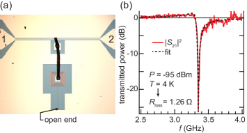
Loss characterization of a wire-bonded coil
We combined same-geometry coils and coplanar transmission lines in a “hanger” configuration (Fig. 5(a)). We then measured at 4 K the power transmission between ports 1 and 2 with dBm (higher than the excitation power used in the experiment). We then fit the curve (Fig. 5(b)) with the formula Pozar (2005):
| (7) |
Here, from Eq. (1) stands for a series cicuit; is a fitting parameter Khalil et al. (2012) that reproduces the asymmetry of the measured curve, caused by external spurious standing waves due to mismatches. The extracted parameters are: , , GHz, . The obtained loss resistance at 4 K is a comfortable upper limit of our 20 mK experiment, mainly because the Al bond wire becomes superconducting and Nb superconductivity gets reinforced in the mK range.
The reduced characteristic impedance in the main experiment as compared to in the hanger is explained by a decreased inductance from the two-turn short in the coil. However, the frequency (and ) is very similar, suggesting that a short can also induce an increase in capacitance. The distributed structure of inductive and capacitive elements in a coil could indeed produce this effect.
Fitting procedure
We extract the unknown circuit parameters , , , and by first fixing a frequency close to the resonance frequency. We then plot the measured reflectance values against the DC measured for the same values of and . This is shown in Fig. 6 as green diamonds. We next assume that is equal to at GHz frequency. Then we can fit a theoretical dependence to the data points, based on Eqs. (1,3,4). Both the dashed orange and full yellow trances in Fig. 6 are candidate fitting curves. The reflectance values at and yield the baseline and ; the lack of the latter value explains why these two parameters cannot be reliably determined simultaneously. We therefore fix ; this choice is also a reasonable in further noise extraction, as is in series with the much larger characteristic impedance of the setup output line.
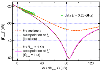
One could be convinced of the low influence of by observing the overlap of the lossless and lossy fits in Fig. 6. In spite of the stability of the extracted parameters in the two fit cases (less than 1 % for and ), it is important to observe in Figs. 2(b), 6 a deviation of the extracted value from the measured one (77 S). Therefore the accuracy of the extracted is at most . In conclusion, working at a fixed frequency outputs effective values of and at that specific frequency, while the analysis of a whole frequency range, if possible, should provide more precise circuit parameters.