Supplemental Material: Andreev Reflection Spectroscopy of Topological Superconductor Candidate NbxBi2Se3
I I. Zero bias conductance
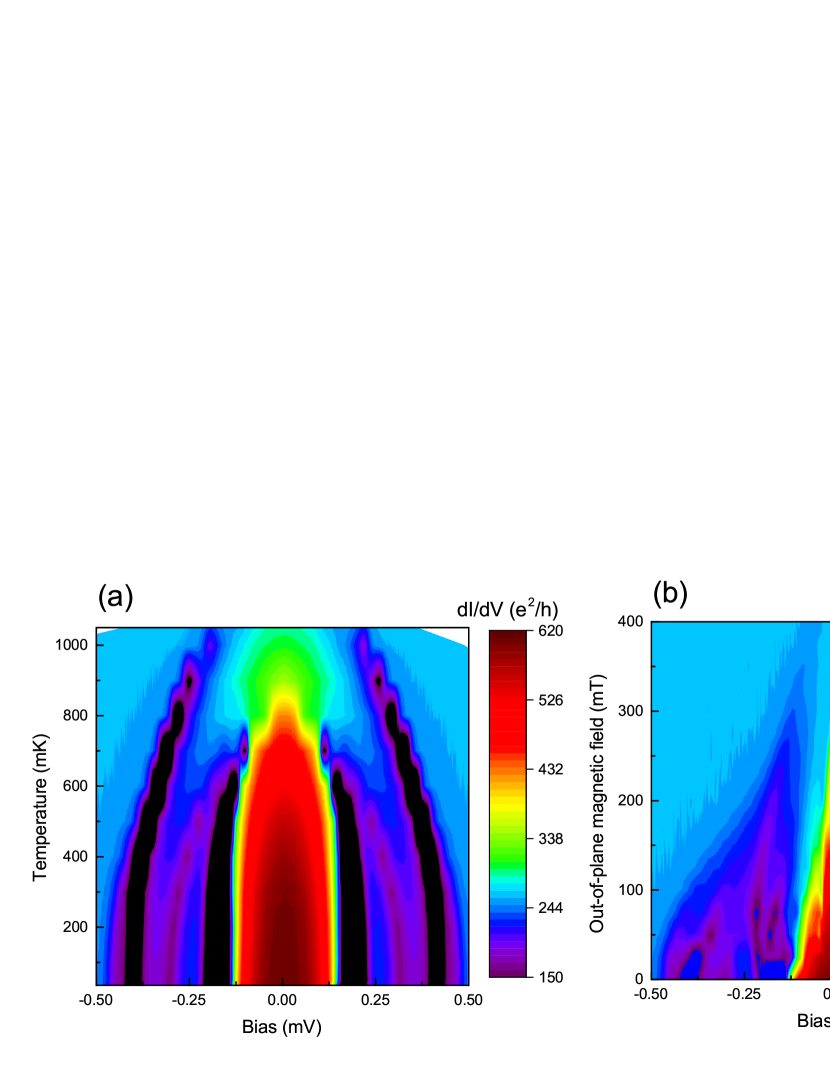
A superconducting device can be treated as a circuit consisting of a resistive element and a superconducting (zero voltage) element. For such a circuit, a finite critical current can generate the appearance of a zero bias conductance peak. When the bias current exceeds the critical current of the superconductor, the device becomes resistive and increases the total circuit resistance. In this picture, the zero bias resistance is equal to that of the resistive element in series with the superconductor, such as contact resistance. We do not expect contact resistance to be strongly dependent on temperature or magnetic field, although the critical current is expected to vary with respect to either such variable. Thus, one would expect the width of the apparent zero bias conductance peak to narrow with increased temperature or magnetic field, but its height should be essentially unchanged.
In Fig. S1, we show color plots of dI/dV vs V as a function of temperature (a) and magnetic field (b) from an Andreev reflection device made with 16 nm thick flake with low contact resistance. We find that zero bias conductance drops steadily with finite temperature or magnetic field, even as the conductance dips at finite bias remain visible. This is in contrast with the simple picture of the zero bias conductance peak originating from finite critical current and supports the hypothesis that the peak is a signature of low energy bound states Sasaki et al. (2011).
II II. Electronic Band Calculations
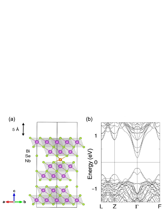
The observation of multiple gaps in some of the measured differential conductance spectra (see Fig. 3) led us to consider that these spectral features might be due to the existence of multi-band superconductivity. We calculated band structures of Bi2Se3 and Nb-intercalated Bi2Se3 slabs by using the generalized gradient approximation in the Perdew-Burke-Ernzerhof form Perdew et al. (1996, 1997). Figure S2(a) shows the electronic structure used in the calculations. To study 2D structures under periodic boundary conditions, a vacuum layer with a thickness of 5 Å was inserted to avoid the interaction between the periodic slabs of rhombohedral Bi2Se3 with three quintuple layers. A single Nb atom (shown in orange) was added either at the surface, inside the top quintuple layer, or between the top two quintuple layers. The energetically preferred location of a single Nb atom within the Bi2Se3 slab was determined using the total energy calculations. Similar to the previous investigations for Nb-intercalated bulk Bi2Se3 Qiu et al. (2016), it is found that Nb prefers to be located between the quintuple layers of the Bi2Se3 slab. For comparison, we first calculated the electronic band structure of Bi2Se3 slab without Nb intercalation as shown in Fig. S2(b).
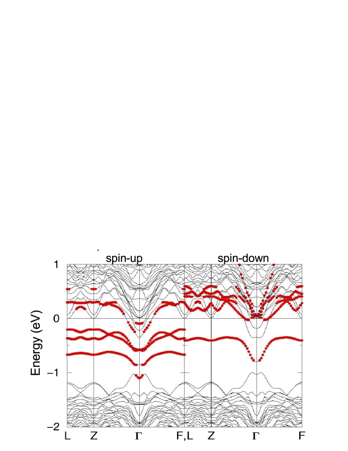
Intoduction of Nb into the slab dramatically changes the band structure as shown in Fig. S3. The occupied Nb states appearing within the band gap of Bi2Se3 below the Fermi energy are highlighted in red; one can see three states for spin-up case and one state for spin-down case. More importantly, Nb states hybridize with the host Bi2Se3 states near the Fermi level resulting in a spin-dependent band structure. The spin-resolved differences near Fermi level suggest previously observed multiple Fermi surfaces Lawson et al. (2016) for Nb-intercalated Bi2Se3, which supports our experimental observations of Andreev conductance spectra with multiple gap features.
References
- Sasaki et al. (2011) S. Sasaki, M. Kriener, K. Segawa, K. Yada, Y. Tanaka, M. Sato, and Y. Ando, Phys. Rev. Lett. 107, 217001 (2011), URL http://link.aps.org/doi/10.1103/PhysRevLett.107.217001.
- Perdew et al. (1996) J. P. Perdew, K. Burke, and M. Ernzerhof, Phys. Rev. Lett. 77, 3865 (1996), URL http://link.aps.org/doi/10.1103/PhysRevLett.77.3865.
- Perdew et al. (1997) J. P. Perdew, K. Burke, and M. Ernzerhof, Phys. Rev. Lett. 78, 1396 (1997), URL http://link.aps.org/doi/10.1103/PhysRevLett.78.1396.
- Qiu et al. (2016) Y. Qiu, K. N. Sanders, J. Dai, J. E. Medvedeva, W. Wu, P. Ghaemi, T. Vojta, and Y. S. Hor, arXiv:1512.03519 (2016).
- Lawson et al. (2016) B. J. Lawson, P. Corbae, G. Li, F. Yu, T. Asaba, C. Tinsman, Y. Qiu, J. E. Medvedeva, Y. S. Hor, and L. Li, Phys. Rev. B 94, 041114 (2016), URL http://link.aps.org/doi/10.1103/PhysRevB.94.041114.