Cryogenic readout for multiple VUV4 Multi-Pixel Photon Counters in liquid xenon
Abstract
We present the performances and characterization of an array made of S13370-3050CN (VUV4 generation) Multi-Pixel Photon Counters manufactured by Hamamatsu and equipped with a low power consumption preamplifier operating at liquid xenon temperature ( 175 K). The electronics is designed for the readout of a matrix of maximum dimension of individual photosensors and it is based on a single operational amplifier. The detector prototype presented in this paper utilizes the Analog Devices AD8011 current feedback operational amplifier, but other models can be used depending on the application. A biasing correction circuit has been implemented for the gain equalization of photosensors operating at different voltages. The results show single photon detection capability making this device a promising choice for future generation of large scale dark matter detectors based on liquid xenon, such as DARWIN.
1 Introduction
Liquefied noble gas targets are at the forefront of the search for dark matter [1, 2, 3]. In the upcoming generation of large scale detectors, a great emphasis will be given to compact photosensors suitable for cryogenic environment, with single photodetection response and allowing for large area coverage [4]. A reduced radioactivity contribution to the total budget in order to minimize the experimental background is also crucial. Direct detection of vacuum ultraviolet (VUV) light is required by liquid xenon (LXe) based experiments () [5], while in liquid argon (LAr, ) a wavelength shifter is usually needed [6]. A wavelength shifter is commonly used to shift the scintillation light towards longer wavelengths [6]. According to the most common WIMP models, the energy released in the interaction between dark and baryonic matter is supposed to be of the order of few tens of keV [7, 8].
To date, photomultiplier tubes (PMTs) are still the most widely used devices for scintillation light collection. In order to reach a more efficient coverage and to reduce the contribution of the photosensors to the total radioactivity budget of the detector, smaller devices are being investigated. With light yields in the liquid phase of the order of a few tens , to be able to achieve enough sensitivity, the detector must have a high geometrical coverage, single photon counting capability, adequate photon detection efficiency (PDE, larger than 20% at the scintillation emission peak) and large gain (in the order of ). A promising candidate is the Silicon Photomultiplier (SiPM) or Multi-pixel Photon Counter (MPPC) [9].
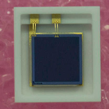
The detector presented in this work is based on the use of the fourth generation of vacuum ultraviolet (VUV) multi-pixel photon counters (VUV4-MPPC) manufactured by Hamamatsu: the S13370-3050CN, shown in figure 1.
The most interesting features of the VUV4-MPPC are listed below:
-
1.
can be operated at low voltage () in LXe,
-
2.
single photon counting capability,
-
3.
PDE close to 25% at ,
-
4.
gain larger than .
To offer the equivalent area of a standard photomultiplier tube while keeping the same number of electronic channels, the grouping of several tens of MPPCs is needed. This requirement poses a challenge in the design of the readout. A few typical readout examples are described in [10]. More specifically, for a detector based on the use of a number of MPPCs, there are three configurations:
-
1.
parallel of MPPCs,
-
2.
series of MPPCs,
-
3.
hybrid: parallels of two (or more) MPPCs connected in series.
The main characteristics of the possible configurations listed above are reported in Table 1.
| Low | Required | DC | |||
| High | Automatic | DC | |||
| Required | AC |
The noise contribution of each MPPC is due to its parasitic capacitance and to the resistance used for the connection to the operational amplifier inverting input.
In the ideal case, for which the parasitic capacitance is extremely low (, the contribution to the overall noise is given by the input voltage noise of the operational amplifier. In the real case, the contribution to the overall noise is given by the number of connected MPPCs, weighed by the ratio between the feedback resistance and . The value is constrained by the characteristics of the operational amplifier in use, while the value has to be optimized.
The challenge is to provide a cryogenic readout that can deal with the capacitance of individual MPPCs, limiting the associated noise and providing a signal to noise ratio larger than one. In Section 2 the detector used in this experiment is described. The experimental setup is shown in Section 3. In Section 4 we describe the readout. The results are presented in Section 5.
2 The detector
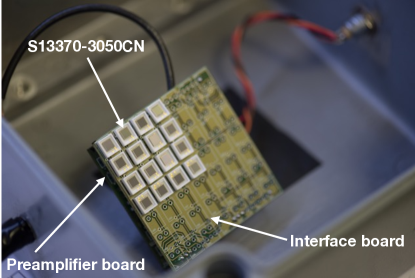
In Figure 2, the prototype of the VUV detector under test is shown. It consists of an array of 16 MPPCs soldered to an interface board that is in turn connected to the preamplifier board.
The decision to split the readout into interface and preamplifier boards has been taken to have the flexibility of testing different types of MPPCs (individually or grouped in tiles). The electronics is designed to readout up to 64 individual channels; however, due to the ceramic frame of the devices under test, the maximum number of S13370-3050CN that can fit on the interface board is in fact 49. For the present work we used 16 MPPCs to have a better characterize the electronics under test.
It is worth mentioning that the AD8011 operational amplifier had been already used by our group, in a preamplifier circuit for the Hamamatsu PMT R11410. The preamplifier was successfully tested at LXe conditions [11].
3 Experimental Setup
The characterization of the detector has been performed at cryogenic conditions and more specifically at LXe temperature () by using a cold finger partially immersed in liquid nitrogen and in direct contact with the setup. Varying the liquid level allows for the control of the temperature. The MPPC array and its electronics have been placed in an aluminum box (see figure 3) equipped with connectors for signal readout, for detector and preamplifier biasing, and with an optical diffuser to isotropically deliver light from a pulsed LED towards the sensitive detector surface. To constantly monitor the temperature and to correct the biasing voltage accordingly, a PT100 has been used. Gas nitrogen has been flushed through the box, to avoid discharges arising from water condensation.
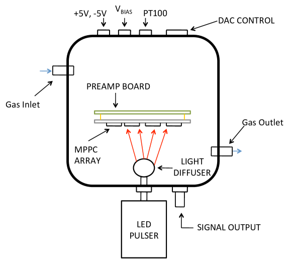
To compensate the effect of different breakdown voltages of the 16 MPPCs, (in the range ) the biasing section has been equipped with a Digital to Analog Converter (DAC) to equalize the over-voltages111 The over-voltage () is the voltage above the breakdown. All the 16 MPPCs have been biased by an Agilent E3645A, while a linear DC Elind 32DP8 power supply has been used to operate the preamplifier. The readout of the temperature through the PT100 has been performed by a Keithley 2100 digital multimeter. A LeCroy HDO6104 high definition oscilloscope has been used for signal readout and data acquisition.
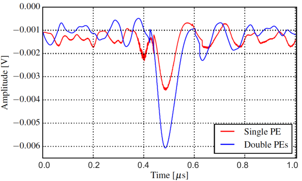
Each waveform has been collected in time window and sampled with 2500 points at 12 bits at full bandwidth. All the results shown in this paper are presented without using any noise or off-line filtering. Examples of waveforms corresponding to single and double photon event families are shown in figure 4.
4 The Electronics
An MPPC can be modeled as a matrix of many independent channels connected in parallel [14], each one consisting of a series of one avalanche photodiode (APD) and one quenching resistor (). Figure 5 shows the typical electrical scheme of an MPPC.
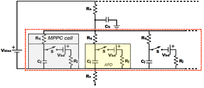
The APD can be represented by a junction capacitance , a voltage source corresponding to the breakdown voltage , a junction resistance and a switch S that closes when a photon hits the sensor. The resistor is then used to quench the signal and restore the APD switch to the open position. Current limiting resistors (), bypass capacitances () and the decoupling resistors () are all wired outside the MPPC.
In Figure 6 two configurations (A and B) for the operation with 16 channels (the electronics can actually host up to 64 devices) are shown. In A, all channels are biased with the same voltage, while B features the additional 8 bit DAC (DAC088S085 by Texas Instruments), suitable for operation at , used to equalize the over-voltage of each channel in steps of . Configuration A is suitable when operating arrays where the breakdown voltage of different cells is highly homogeneous, otherwise configuration B must be used.
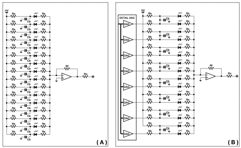
Both circuits have been designed to prevent any contribution of non-fired MPPCs to the analog signal sum of the entire array. An approach similar to configuration A was considered for liquid argon based applications, but with a different detector [12, 13].
The resistor is used to decouple the MPPC equivalent parasitic capacitance of any non-fired photosensor from the operational amplifier. The presence of is what makes this design different from a purely parallel configuration. This technique becomes highly effective at low temperature where the dark counting rate drops dramatically.
Figure 7 is an approximate representation of the array when a MPPC (MPPC number 0) detects a photon (is ‘fired’) while the others don’t.
The MPPC-0 signal is represented by the current generator connected in parallel with towards ground. is equivalent to the parallel of the of each cell composing the MPPC. It is worth mentioning that all the quenching resistors are connected in parallel, resulting in an equivalent resistance that is negligible with respect to . Due to a series connection between and the equivalent quenching resistance, its effect can be also included in the overall effect of . The operational amplifier output voltage is, to first order, the product between the value of the feedback resistance () and the current , given the negligible effect of and .
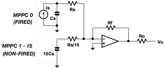
The average amplitude of a typical single photon event waveform (, , see Figure 4) is 2.5 mV corresponding to ( and ).
4.1 Gain equalization
The analog sum of signals generated by individual devices operating at different over-voltages will affect the single photon detection capability of the entire array because of the non-uniformity of the gain. By using the configuration B reported in figure 6, the over-voltage of each MPPC group can be fine tuned, resulting in the equalization of the gains, without contributing to the overall noise. Each DAC serves 2 (or more) MPPCs with similar breakdown voltages. Two resistors, and are used to distribute, respectively, the biasing voltage and the DAC output.
The biasing voltage is given by the following equation:
| (1) |
where is the operating voltage of the MPPC, while and are the output voltages of the DAC and of the power supply. The maximum output voltage of DAC used in the setup is that allows for a biasing correction in the range of . The and values are constrained by the equation:
| (2) |
This configuration preserves the DC coupling of the MPPCs, with a slight increase of the total power budget, as shown below:
| (3) |
Using and in the DAC configuration, the biasing voltage becomes:
| (4) |
The power consumption can be reduced by increasing the value of the distribution resistors , as shown in Table 2.
| 0.25 | 1 | 55.5 + 1.0 = 56.5 | 2.5 | 70 | 3.65 |
| 2.5 | 10 | 55.5 + 1.0 = 56.5 | 2.5 | 70 | 0.36 |
| 5 | 20 | 55.5 + 1.0 = 56.5 | 2.5 | 70 | 0.18 |
The number of DACs used in the proposed configuration can be reduced if the MPPC breakdown voltage spread is small enough. The more MPPCs connected to a single DAC, the lower the overall power absorbed. In the present configuration, each DAC serves 2 MPPCs only, but considering the narrow span of breakdown voltages of the sample, more devices could be connected to a single DAC channel.
4.2 Noise Model
The non-correlated noise sources considered in the design of the circuit are shown in Figure 8. The AD8011 is a current feedback operational amplifier, however the proposed circuit has been studied and operated as a transimpedance amplifier (TIA). This assumption is considered valid, as reported in [15]. and represent the noise voltage contributions of resistors and . is the parasitic capacitance of a MPPC. and are the input noise voltage and current of the AD8011. The input and output operational amplifier voltages are and , respectively, while is the amplifier open loop gain value.
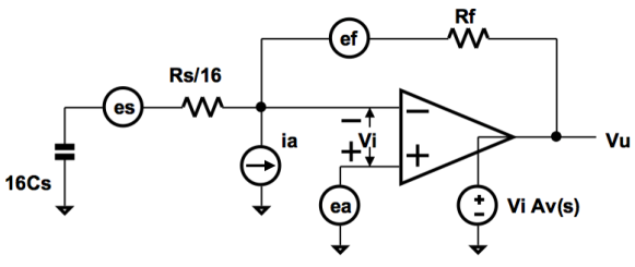
The impedance of all the input branches, expressed in terms of the complex variable in the Laplace transform space, is given by the following equation:
| (5) |
To account for the overall noise contribution, the transfer functions of each uncorrelated noise source have been evaluated, and added quadratically. To estimate the total noise effect, we run a simulation assuming infinite input impedance and open loop gain with finite value and dominant pole. The system has been modeled as a voltage-feedback amplifier for the analysis of the total noise.
The transfer function of each noise source in the Laplace space can be written as:
| (6) |
where is the noise source (), is a factor specific for each source and is a common component to all the transfer functions.
Each transfer functions can be expressed in the frequency domain by replacing the Laplace variable with the complex expression , where f is the frequency.
for each noise source is reported in Table 3. The contribution of the input voltage noise is the most significant.
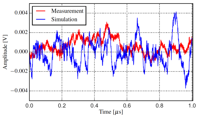
The simulation has been performed by transforming the transfer functions from the Laplace s-domain to the z-transform domain resulting in a recursive equation in the time domain. The solution of the equation, once set the boundary conditions, is a waveform that can be compared to the measured one. Due to the intrinsically random process, simulated and measured waveforms should be only compared qualitatively.
Time domain simulated and acquired noise waveforms (taken at room temperature) are shown in Figure 9. The RMS evaluated for real waveforms, over a sample of 10,000 events taken at , is of the order of . The RMS of simulated waveforms is .
5 Results
To test the single photon detection capability of our system, we have operated the array (with 16 MPPCs) in configuration A (see figure 6), , and illuminated by a pulsed UV LED. The measurements have been performed at low intensity to maximize the probability of having only one photon per event (see figure 10) and at a higher intensity for the detection of several photons per event (see figure 12).
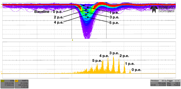
The separations of signal families corresponding to different number of photons detected in a single event is shown in figure 10, where the waveforms have been acquired in persistence mode. The first family, below the baseline band, corresponds to events triggered by single photons, the second family to events triggered by two photons, etc. The corresponding integrated values in the window centered around the signal peak are shown in figure 10 (bottom).
The photoelectron spectrum has been therefore fitted with a set of multiple gaussians (see figure 11): the measured charge of the pedestal is , while the single photoelectron peak is found at about , corresponding to an overall gain of (, ).
Since the sigma of the charge pedestal showed in figure 11 is smaller than the average charge separation between two consecutive peaks ( versus ), a distinctive photoelectron peak charge distribution can be observed. Assuming no statistical effects, the main contributions to the sigma of each photoelectron peak are in fact due to noise (), dark counts (), afterpulses (), crosstalk () and gain fluctuation (): the corresponding integrated charge of any signal emerging from the tail of a spurious event (AP, CT or DC) is slightly overestimated if compared to a signal rising from the baseline.
The equation:
| (7) |
Since of the first photoelectron peak is and is , the contributions due to the detector (AP+DC+CT+GF) is dominant (). By improving the gain uniformity (using configuration B in figure 6 and the MPPC characteristics), we could conclude that the maximum number of MPPCs used in the array and readout as a single channel can be increased.
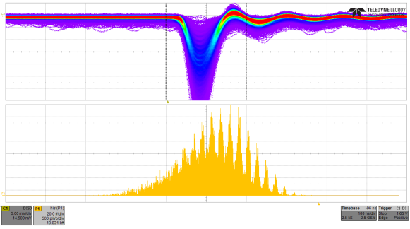
Figure 12 (top) shows waveforms acquired in persistence mode when operating the LED at high intensity, and .
In comparison with figure 10, a higher number of families can be identified and their separation is still preserved. The charge spectrum of the acquired signals is shown in figure 12 (bottom).
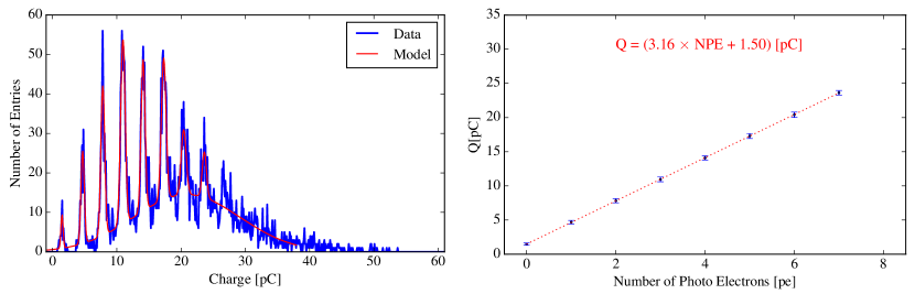
To quantify the linearity of the device, a fit with a set of 14 Gaussian functions has been applied to the acquired data (Figure 13, left).
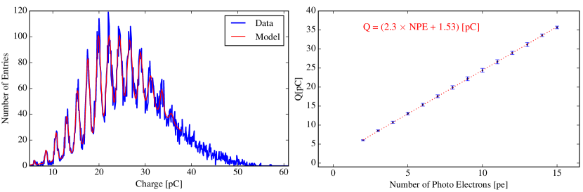
The charge value of each peak is reported as a function of the number of detected photons (see Figure 13, right). The gain of the photodetector while the the average charge separation between to consecutive photopeaks is , the corresponding gain is .
5.1 241Am spectrum using a LYSO crystal.
To evaluate its spectroscopic capabilities, the array was coupled to a Lutetium-Yttrium Oxyorthosilicate (LYSO) crystal irradiated by a 241Am source (, ). The charge spectrum is shown in figure 14, where the 59.6 keV 241Am gamma peak and the intrinsic LYSO background spectrum due to are clearly visible.
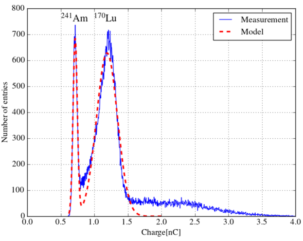
The measured charge in correspondence of the 59.6 keV line is (corresponding to about ). The LYSO light yield is about 30 photons/keV [16], that is about for the 59.6 keV gamma emission from 241Am. Taking into account the photo-electron conversion efficiency, the geometrical coverage of the crystal and non optimal crystal coupling, an overall photon detection efficiency of the order of is plausible. The estimated energy resolution at the 59.6 keV line is .
6 Conclusions
The aim of this work is to provide LXe detectors, searching for WIMP-nucleus interactions, the possibility of using MPPCs for the direct detection of scintillation VUV light.
The array, made of 16 individual Hamamatsu VUV4 MPPCs (S13370-3050CN), operates as a single detector by means of a board based on an operational amplifier suitable for cryogenic environments (AD8011). The total power consumption is about per array.
The electronics foresees a configuration based on the use of Digital to Analog Converter (DAC). This configuration is more demanding in terms of power supply ( per DAC channel), but it increases the single photon counting capability by compensating the gain differences between MPPCs operating at the same biasing voltage.
The noise analysis demonstrated that the only relevant source of noise for the proposed electronics is given by the voltage noise of the input of the operational amplifier.
The measurements show an excellent photo detection capability. Overall, the performance of this device seems to be promising enough to warrant further studies for its use in liquid xenon based detectors.
References
- [1] Akerib, D. S. et al.: Signal yields, energy resolution, and recombination fluctuations in liquid xenon - Phys. Rev. D 95, 012008
- [2] Abe, K. et al.: XMASS detector - Nuclear Instruments and Methods in Physics Research A716 (2013) 78-85
- [3] Agnes P., et al.: First results from the DarkSide-50 dark matter experiment at Laboratori Nazionali del Gran Sasso - Physics Letters B, 743 (2015): 456-466
- [4] Baldini, A. et al.: DARWIN: towards the ultimate dark matter detector - JCAP11(2016)017
- [5] Aprile, E. et al.: Physics reach of the XENON1T dark matter experiment - JCAP04(2016)027
- [6] Burton, W., Powell, B.: Fluorescence of tetraphenyl-butadiene in the vacuum ultraviolet - Journal of Applied Optics 12 (1973).
- [7] Goodman, M.W., Witten, E.: Detectability of certain dark-matter candidates - Phys. Rev. D, 31 (1985), p. 3059
- [8] Wasserman,I.: Possibility of detecting heavy neutral fermions in the Galaxy - Phys. Rev. D, 33 (1986), p. 2071
- [9] Yamamoto, K., Yamamura, K., et al.:Development of Multi-Pixel Photon Counter (MPPC) - 2006 IEEE Nuclear Science Symposium Conference Record N30-102
- [10] Sawada, R: Upgrade of MEG Liquid Xenon Calorimeter - Proceedings of Science (TIPP2014) 033
- [11] Arneodo, F., Benabderrhamane, M.L. et al.: An amplifier for VUV photomultiplier operating in cryogenic environment. - Nuclear Instruments and Methods in Physics Research A 824 (2016) 275–276
- [12] Catalanotti, S., Cocco, A.G. et al.: Performance of a SensL-30035-16P silicon photomuliplier array at liquid argon temperature - 2015 Jinst 10 P08013
- [13] D’Incecco, M., Galbiati, C. et al.: Development of a novel single-channel, 24 cm2, SiPM-based, cryogenic photodetector - arXiv:1706.04220
- [14] S. Piatek, Measuring the electrical and optical properties of the MPPC silicon photomultiplier (February 2014), Internal Note, www.Hamamatsu.com
- [15] Application Report, SNOA376B–July 1992–Revised April 2013, http://www.ti.com/lit/an/snoa376b/snoa376b.pdf
- [16] Phunpueok, A., Chewpraditkul, W. et al.: Light output and energy resolution of and scintillators - Procedia Engineering Volume 32, 2012, Pages 564-570