Interaction between counter-propagating quantum Hall edge channels in the topological insulator BiSbTeSe2
- Supplemental Material
Abstract
1. Quantum Hall effect comparison
2. Sample fabrication
3. Gate-dependent hysteresis
4. Determining the Landau levels
5. Multiband fitting results
6. Landau level spacing and effective dielectric constant
7. Landauer-Büttiker formalism for topological insulator quantum Hall edge states
8. (Anti-)symmetrization of and signals in the dissipative quantum Hall regime
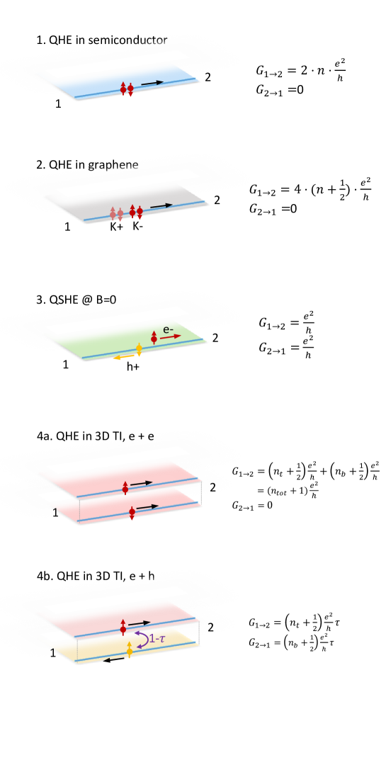
.1 1. Quantum Hall effect comparison
In this section, an overview is given over the different versions of the quantum Hall effect in different materials, and the possible values for the quantized mode conductances in the different cases, see also Fig. S1. A spin-degenerate semiconductor has two conductance quanta per mode because of spin. The modes run in the direction as dictated by the magnetic field. Graphene has an additional degeneracy factor of two because of the valley degeneracy. The Dirac type of dispersion in graphene has an associated pseudospin-momentum locking that provides an offset of . This zeroth Landau level is also refered to as a consequence of the non-zero Berry phase in a Landau orbit. The -term is an exciting illustration of how a non-trivial topological number appears in the quantum Hall language of topological TKKN quantum numbers. The quantum spin Hall insulator lacks this factor of . The quantum spin Hall insulator has counterpropagating modes, hence conductance in both directions. The spin is opposite for the two directions, hence the modes are quantum mechanically orthogonal and no elastic scattering between the modes is allowed. For the three-dimensional topological insulator, the mode direction is determined by the magnetic field and the nature of the carriers (electrons when the chemical potential lies above the Dirac point, holes when the chemical potential is below the Dirac point). Co-propagating modes have opposite spin (because the helicity is reversed for the top and bottom surfaces) and a factor of because of the helical spin-momentum locking in the Dirac cone. Counter-propagating modes have the same spin and scattering between the modes is quantum mechanically allowed. The transparency of the mode, , can then be smaller than one.
.2 2. Sample fabrication
High quality BiSbTeSe2 single crystals were grown using a modified Bridgman method. Stoichiometric amounts of the high purity elements Bi (99.999%), Sb (99.9999%), Te (99.9999%) and Se (99.9995%) were sealed in an evacuated quartz tube and placed vertically in a tube furnace. The material was kept at 850 ℃ for three days and then cooled down to 500 ℃ with a speed of 3 ℃ per hour, followed by cooling to room temperature at a speed of 10 ℃ per minute. We exfoliated single crystal flakes onto a highly doped silicon substrate topped with a 300 nm thick SiO2 layer on top. Nb/Pd (80/10 nm) metal contacts are fabricated using sputter deposition and e-beam lithography. After making the contacts, we shaped the flakes into a Hall bar structure using e-beam lithography and Ar+ etching. Next, the entire central area of the BiSbTeSe2 flake is covered with a 20 nm thick Al2O3 layer using atomic layer deposition at 100 ℃. In the final step, the top gate is realized by using e-beam lithography and lift-off of a sputter deposited Au layer. Two devices have been characterized at low magnetic fields and both show similar behavior. One device was selected for the high-magnetic field measurements. Fig. 1 depicts the schematic layout of the experiment as well as an optical microscopy image of the device.
.3 3. Gate-dependent hysteresis
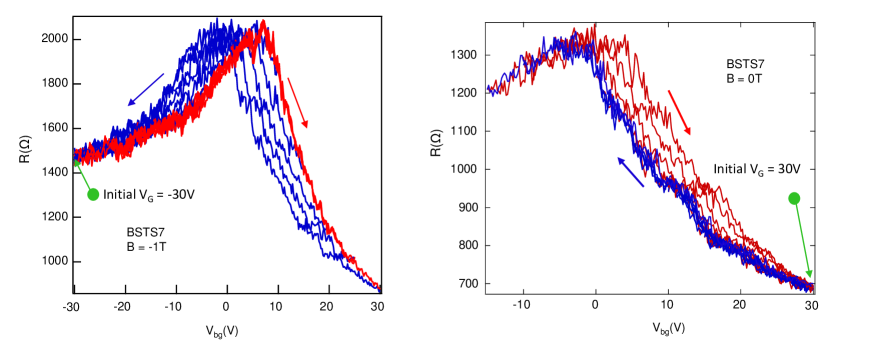
For both surfaces, gate-dependent sweeps show hysteretic behavior. The hysteresis is probably mainly due to trapped charges in bulk defects, which do not contribute to the transport. By carefully comparing the data of up and down sweeps, we find that the curves are fully reproducible for identical initial conductions and sweeping direction. In Fig. S2, we show a series of representative gate voltage sweeps. All curves with the same initial state, and the same sweeping direction exactly retrace. This memory-like behavior is observed consistently in all of our samples for both top and bottom gating.
.4 4. Determining the Landau levels
This section deals with how one can determine the filling factors for each surface if the LLs are not fully quantized. First, we use our low field results. We determine the gate voltage, , at which the charge carrier density is the lowest by changing only one gate voltage. Normally, this point corresponds to the maximum of . Once the Fermi level crosses the Dirac point, the signal changes sign and a large peak or dip is observed in the measured differential resistance. Such a significant change in signal gives a clear indication of the and LLs (depending on the sign of the gate voltage). In this way, we located four levels at -40V and -55V for the , and V and -3V for respectively. Here, the labels t [b] represent the top [bottom] surface. After assigning these filling factors, we can determine the filling factors of the other squares in the gate map, shown in the main paper in Fig. 3(a).
.5 5. Multiband fitting results
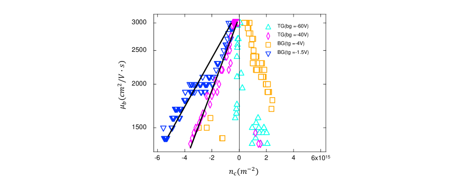
For the fitting of the low-field Hall data, as presented in Fig. 2 of the main text, a two- or three-band model was used. The curves and the zero field longitudinal resistance values were used to obtain the carrier density and mobility values for both the top and bottom surfaces. The third band that was used to fit the data is ascribed to charge puddles and only plays a role when is close to . In Fig. S3, we show the fitting results for different gate voltages.
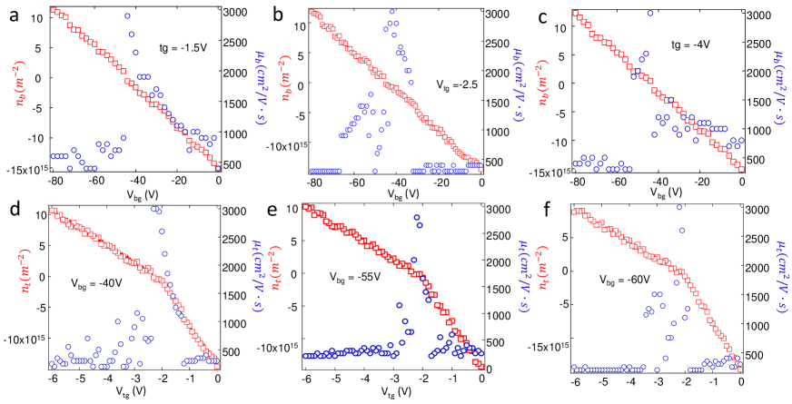
As a guideline for the fitting, the carrier density of the gated surface was only allowed to change linearly with the gate voltage. The rate of change was determined using the effective dielectric constants obtained from the LL fan diagrams discussed in Supplementary Section 5 below. For the other surface and the charge puddles, a small range in carrier density was chosen such that the data could be well fitted across the gate voltage range. However, the mobility of the gated surface was allowed to vary distinctly more, since the mobility increases significantly close to the Dirac point, as shown in Fig. S3.
It is evident that the bulk conductivity does not appear to be relevant in the data fitting. This observation was already warranted from the independent gate tuning of the top and bottom surfaces. We argue here that bulk conductivity is also negligible when it comes to equilibration between electrodes. The independent gating, as shown in main text Fig. 1(b), implies a negligible conductance between the top and bottom surfaces on the scale of the longitudinal conductance. Given the order of magnitude of the longitudinal resistance, of 10 k, and the dimensions of the Hall bar (i.e. a flake thickness of 240 nm, a width of about 1 m and a length of more than 5 m), the bulk resistivity is then found to be much larger than 2 cm. The bulk channel resistance between electrodes (spacing is 2 m) is then found to be much larger than 2 , meaning that it can be neglected when compared to the quantum of the resistance.
The increased mobility close to the Dirac point is similar to what has been reported for (Bi0.04Sb0.96)2Te3 TianSciRep2014 , BiSbTeSe2 (see supplementary material of Ref. XuQHE, ), and also for graphene HighMobsuspendedGraphene . Multiple scattering mechanisms can be responsible for such a carrier density dependent mobility GauravSciRep2014 ; DohunPRL2012 : defects on the topological insulator surfaces, phonons, or even edge roughness. Experimentally, near the Dirac point, we observe a logarithmic dependence of the mobility on the carrier density with different pre-factors that depend on the gate voltage used. The observed kink in the dependence of the top-surface carrier density on top-gate voltage must relate to a change in gating efficiency across the Dirac point, likely related to a change in dielectic screening.
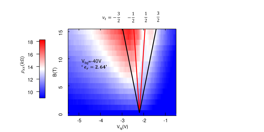
.6 6. Landau level spacing and effective dielectric constant
In a Dirac cone, the energy of the LLs is given by . Considering that the degeneracy of the spin is lifted for the 2D topological surface states, we get a density of states of . Using , we can deduce the number of carriers per unit area for each surface as function of the gate voltage,
| (1) |
We found that if we use the ideal dielectric constant for the Al2O3 top gate and the SiO2 bottom gate, the field dependence of the calculated LLs does not fit our experimental results. Therefore, we try to fit the ‘Landau fan diagram’ using an effective dielectric constant, . In this way, we get a good fit with for the Al2O3 top gate and for the SiO2 bottom gate, which are used in previous section of this paper to obtain boundary conditions for the two-band fits. Note that when the theoretical lines fit the fan diagram well, the spacing between different LLs should also fit the data (Fig.S5), confirming the chosen effective dielectric constant. The reduced dielectric constant has also been observed in previous experiments with BiSbTeSe2 (see supplementary material of Ref. XuQHE, ).
.7 7. Landauer-Büttiker formalism for topological insulator quantum Hall edge states
In a Hall bar, see for example Fig. 1(a) in the main text of the paper, the edge states provide a quantized value of the Hall conductance . In a current biased Hall bar, the Hall conductance relates to the measurable transverse resistance and the longitudinal resistance by .
In general, to calculate device conductances from edge states, the Landauer-Büttiker formalism is well suited. All device terminals, assumed to be leads that are in equilibrium with potential , are labeled with and index. The current into (positive) or out of (negative) a terminal is then given by
| (2) |
where are the values for the edge conductance from terminal to . This equation can be converted into a matrix equation that relates current, , to voltage, . Putting the current values into then allows to solve for all the elements of . With the definitions of and one then obtains the conductances and .
The top and bottom surface of a 3D topological insulator have Dirac cones with opposite helicities. Therefore, when the two surfaces are gate-tuned to both have the Fermi energy above or below the Dirac point (i.e. two electron or two hole Fermi surfaces), the edge modes of the two surfaces propagate in the same direction but are orthogonal and no scattering from one to the other is quantum mechanically allowed. Therefore, the mode conductances add up in the elements of , e.g. . It is then straightforward to show that .
However, when the two surfaces of a topological insulator are gate-tuned at different sides of the Dirac point (i.e. one electron and one hole Fermi surface), the edge modes of the two surfaces are counter-propagating. In this case, the helicities of the states are equal (the sign reversal going from the top to the bottom surface is cancelled by the sign reversal going from the electron to the hole side of the Dirac cone). Here, we will derive a model for the interaction between the modes, but first we focus on the case of negligible coupling, such as is the case for a sufficiently thick topologial insulator for which the surfaces are far apart. In contrast to the QSH case which has only one mode in each direction, the counterpropagating modes in a topological insulator can consist of higher values of . For example, the case of and gives values of and , etc. Solving the Landauer-Büttiker equation then for a standard six-terminal Hall bar, quite surprisingly, provides a non-integer quantized value for . For example, the case with counter-propagating modes given above provides . Quantum Hall conductance values for other filling factors are mentioned in Fig. 3(b) of the main text.
Now we take also the coupling between modes into account. We introduce a transmission parameter for modes that have a counterpropagating partner at the other surface. Since modes that orginate from different Landau levels are orthogonal in real space, we neglect scattering between them. As an example, we take again the case of and case for which we then consider scattering only between the and terms. The mode conductance at the top surface then becomes instead of . When the electrodes are numbered from 1 to 6 clockwise around a six-terminal Hall bar, then the conductance matrix becomes
| (3) |
Combining Eqs. (2) and (3) then gives
| (4) |
where . Putting then allows to solve the matrix equation and from which can then be calculated as a function of . For example, for , as mentioned in the main text of the manuscript, a value of is obtained. For the case of decoupled modes (in this context a thick topological insulator), there is no scattering between the modes and, therefore, , giving . A very strong coupling can be modelled by taking , which effectively localizes the lowest modes at the two surfaces, excluding them from the conductance. The conductance is then . Also for higher order filling factors the integer quantization is restored again for , due to the cancellation of the modes.
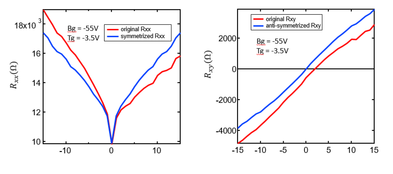
.8 8. (Anti-)symmetrization of and signals in the dissipative quantum Hall regime
In Fig. S6, we show an example for the symmetrization and anti-symmetrization as used in the main text. The is not fully quantized and the does not fall to zero, not even when the states are parallel-propagating. Even in the ideal case, due to the dissipative nature of the edge channels when counter-propagating, can be particularly large (see section above), giving rise to a possible admixture of and signals when contacts are slightly mis-aligned. Hence the need for (anti-)symmetrization in general.
To correct the geometry effect in the Hall-bar sample, we symmetrized the signal with and anti-symmetrized the signal with . Then we use and to obtain the longitudinal and transverse conductance.
References
- (1) J. Tian, C. Chang, H. Cao, K. He, X. Ma, Q. Xue, Y.P. Chen, Sci. Rep. 4, 4859 (2014).
- (2) Y. Xu, I. Miotkowski, C. Liu, J. Tian, H. Nam, N. Alidoust, J. Hu, C.K. Shih, M.Z. Hasan, Y.P. Chen. Nature Phys. 10, 956 (2014).
- (3) K.I. Bolotin, K.J. Sikes, Z. Jiang, M. Klima, G. Fudenberg, J. Hone, P. Kim, H.L. Stormer, Sol. State Comm. 146, 351 (2008).
- (4) G. Gupta, M. Jalil, Bin Abdul, G. Liang, Sci. Rep. 4, 6838 (2014).
- (5) D. Kim, Q. Li, P. Syers, N.P. Butch, J. Paglione, S. Das Sarma, M.S. Fuhrer, Phys. Rev. Lett. 109, 166801 (2012).