Decay Rate of Magnetic Dipoles near Non–magnetic Nanostructures
Abstract
In this article, we propose a concise theoretical framework based on mixed field-susceptibilities to describe the decay of magnetic dipoles induced by non–magnetic nanostructures. This approach is first illustrated in simple cases in which analytical expressions of the decay rate can be obtained. We then show that a more refined numerical implementation of this formalism involving a volume discretization and the computation of a generalized propagator can predict the dynamics of magnetic dipoles in the vicinity of nanostructures of arbitrary geometries. We finally demonstrate the versatility of this numerical method by coupling it to an evolutionary optimization algorithm. In this way we predict a structure geometry which maximally promotes the decay of magnetic transitions with respect to electric emitters.
pacs:
68.37.Uv Near-field scanning microscopy and spectroscopy78.67-n Optical properties of low-dimensional materials and structures
73.20.Mf Collective excitations
I Introduction
During the last two decades, the development of nano-optics has provided a wealth of strategies to tailor electric and magnetic fields down to the subwavelength scale Novotny and Hecht (2006). In particular, optical nano-antennas have allowed to modify the intensity, dynamics or directionality of light emission from fluorophores placed in the near-field of nano-objects using concepts from the radiofrequency domain Anger et al. (2006); Kühn et al. (2006); Kinkhabwala et al. (2009); Curto et al. (2010); Biagioni et al. (2012); Novotny and van Hulst (2011); Klimov et al. (1996). These studies have been performed nearly exclusively on fluorophores supporting electric dipole (ED) transitions, the latter being larger than their magnetic dipole (MD) counterpart in the optical frequency range ( being the Bohr radius and the transition wavelength) Giessen and Vogelgesang (2009). Recently, delicate experiments have addressed light emission from rare earth doped emitters supporting both strong MD and ED transitions Aigouy et al. (2014); Choi et al. (2016). Three–dimensional maps of the luminescence of Eu3+ doped nanocrystals scanned in the near-field of gold stripes have revealed variations in the relative intensities of ED and MD transitions Karaveli and Zia (2011); Aigouy et al. (2014). In these experiments, the fluorescence intensity, photon statistics and branching ratios are directly related to the decay rates of the ED or MD radiative transitions, the latter being ultimately connected to the electric or magnetic part of the local density of electromagnetic states (EM-LDOS) Aigouy et al. (2014); Carminati et al. (2015); Baranov et al. (2017); Cuche et al. (2017). Independently of the nature of the transition, the alteration of the EM-LDOS by a nanostructure arises from the back action of the electric or magnetic field on the transition dipole Purcell et al. (1946); Chicanne et al. (2002); Anger et al. (2006); Rolly et al. (2012); Chigrin et al. (2016).
Analytical expressions for the decay of magnetic transitions have been derived for the simple case of single Chew (1979); Klimov and Letokhov (2005); Schmidt et al. (2012) or also multiple spheres Stout et al. (2011); Rolly et al. (2012). For more complex geometries or arrangements of nano-structures, standard numerical tools like finite difference time domain (FDTD) or finite elements method (FEM) can be employed to calculate magnetic decay rates. To do so, a kind of numerical experiment is performed where the radiated power of a dipole emitter is compared for the cases with, and in absence of a nanostructure. Feng et al. (2011); Hein and Giessen (2013); Albella et al. (2013); Mivelle et al. (2015); Feng et al. (2016)
Whereas, the underlying physics is well understood, a unified description of the dynamics of a fluorophore supporting MD transitions in the presence of non-magnetic nanostructures of arbitrary shape is still lacking.
The confinement of the magnetic field around non-magnetic nano-objects arises from the spatial variations of the electric near–field in the immediate proximity of a nanostructure. When the surface is illuminated by a plane wave or an evanescent surface wave, both experimental data and numerical simulations reveal spatial modulations in the electric and magnetic near-field intensities. For example, the magnetic field intensity recorded above subwavelength sized dielectric particles, excited by a p–polarized surface wave, has a strong and dark contrast while a completely opposite behavior is observed for the electric field intensity Burresi et al. (2009); Devaux et al. (2000a, b). If now, the nanostructure is illuminated, no longer by a plane wave but by a dipole source, the response fields (electric or magnetic) are different and shape the decay rate and the corresponding dipolar luminescence. From a mathematical point of view, the magnetic near-field can be described by a set of mixed field–susceptibilities capable of connecting an electrical polarization, oscillating at an optical frequency , to a magnetic field vector oscillating at the same frequency Girard et al. (1997); Schröter (2003). In fact, these field–susceptibilities are a generalized form of the usual Green dyadic tensor Martin et al. (1995); Girard (2005). Historically, they were introduced by G.S. Agarwal to describe energy transfers in the presence of dielectric or metallic planar surfaces Agarwal (1975). Mixed field–susceptibilities can be used to evaluate the optical magnetic near-field or the optical response of nano-structures possessing an intrinsic magnetic polarizability, like metallic rings or split-rings. Schröter (2003); Sersic et al. (2011) In recent works, they have been used to separately study the magnetic and electric part of the LDOS close to a surface Kwadrin and Koenderink (2013) and for the calculation of the EM-LDOS in proximity of periodic arrays of magneto-electric point scatterers Lunnemann and Koenderink (2016).
In this article, we first extend Agarwal’s theory by presenting a new analytical scheme yielding the total decay rate of a MD transition in terms of mixed electric–magnetic field–susceptibilities. From this concise mathematical framework, we develop a flexible and powerful numerical tool to compute the decay rate of magnetic dipoles near dielectric or metallic nanostructures of arbitrary shapes (see example in Fig. 1). In a second step, we explore the decay rate maps generated by the coupling between rare–earth atoms and dielectric nanostructures. We highlight and discuss the differences between electric and magnetic decay rate topographies. Finally, we demonstrate the versatility of our mathematical framework by coupling it to an evolutionary optimization algorithm to predict a metallic nano-structure yielding an optimum contrast between the magnetic and electric parts of the EM-LDOS.
II Magnetic field-susceptibility for non-magnetic structures
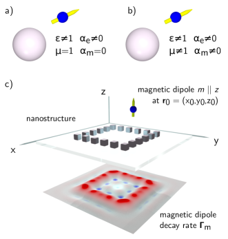
The two possible kinds of coupling between a magnetic dipole transition and a subwavelength sized sphere are schematized in figure 1-a and b. The first one is the coupling with a standard material (bulk metal, dielectric or semiconductor) which does not possess any intrinsic magnetic response (i.e. for which the magnetic permeability is equal to unity (CGS units)) while the second one is the direct magnetic coupling such as the one involved in the presence of artificial left–handed materials, i.e materials with simultaneously negative permeability and permittivity Pendry (2000); Soukoulis et al. (2007). We address exclusively the first situation and therefore assume that = 1 at all wavelengths. We consider the geometry depicted in figure 1. The electric and magnetic fields generated at by a magnetic dipole located at are defined by Agarwal (1975):
| (1) |
and
| (2) |
where is the wave vector in vacuum and = represents the scalar Green function. From these two equations, we can define two field susceptibilities:
| (3) |
and
| (4) |
in which the dyadic tensors and are constructed by identification with equations (1) and (2). For the mixed dyad this identification yields the expression of the nine analytical components:
| (10) |
Equations (1) and (2) define the so–called illumination field. Since the materials considered in this article do not directly respond to the optical magnetic field, the coupling with the nanoparticle is entirely described by the first equation. A complete theoretical investigation of this illumination mode requires the accurate computation of the optical field distribution inside the nanostructure for every location of the magnetic dipole. As discussed in the literature, the recent developments of real space approaches for electromagnetic scattering and light confinement established powerful tools for the calculation of the electromagnetic response of complex mesoscopic systems to arbitrary illumination field Girard (2005). Particularly, the technique of the generalized field propagator described in reference Martin et al. (1995), provides a convenient basis to derive the electromagnetic response of an arbitrary system to a great number of different external excitation fields Arbouet et al. (2014). Our approach is based on the computation of a unique generalized field propagator that contains the entire response of the nanostructure to any incident electric field . Consequently, the self-consistent electric field created inside the nanosystem by a magnetic dipole located at , can be written as:
| (11) |
in which the integral runs over the volume of the particle. As demonstrated in reference Martin et al., 1995, the dyadic writes
| (12) |
where is the three-dimensional Dirac function, is the optical field–susceptibility tensor of the nanostructure of electric susceptibility .
Equation (11) gives access to the electric field inside the nanostructure and therefore to the polarization induced for each position of the magnetic dipole. The magnetic field generated outside of the particle can then be calculated by introducing the second mixed field–susceptibility Agarwal (1975):
| (13) |
which, in a concise form, leads to:
| (14) |
where defines the magnetic field susceptibility associated with the nanostructure :
| (15) |
Here, the dot “” signifies the matrix product. This general relationship, derived from the theory of linear response, brings to light the complex link between the electrical response of matter (contained in and ) and the magnetic response of vacuum, through the mixed propagators and . The combination of these response functions shows in a concise way how a nano-structure, which originally does not possess any magnetic response in the optical spectrum, can nevertheless yield a magnetic–magnetic response. Equation (15) summarizes with mathematical clarity the back-action of the electromagnetic near-field on a magnetic quantum emitter via the curl of the electric field, mediated by the presence of a non-magnetic nanostructure.
III Magnetic dipole decay-rate close to small dielectric particles
Equation (15) allows us to obtain a general expression for the decay rate associated with a magnetic dipole transition of amplitude Carminati et al. (2015):
| (16) |
where = represents the natural decay rate of the magnetic transition and labels the dipole orientation.
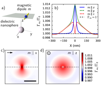
The next objective of this article is to supply a full analytical treatment of . To achieve this goal, we deliberately reduce the physical model to a simple two–level system coupled to a single spherical nanoparticle as shown in figure 2-a. We have chosen to illustrate our method with dielectric materials as they offer an interesting alternative to metals with reduced dissipative losses and large resonant enhancement of both electric and magnetic near-fields Bakker et al. (2015); Decker and Staude (2016); Kuznetsov et al. (2016).
In this case, a set of simple analytical equations can be derived that include all the physical effects mentioned above. Indeed, we have = ( being the identity tensor), = , where is the dynamical dipolar polarizability of the sphere, and finally:
| (17) |
This relation can be further simplified by replacing both and by their analytical expressions. In a plane defined by , i.e. = , we get the following simple expression when = (c.f. equation (16)):
| (18) |
where and the matrix is defined by:
| (24) |
In consequence, has the dimension of an inverse volume.111 has a dimension of , of and all terms in the curly brackets of Eq. (18) are homogeneous to A concise expression of the normalized magnetic decay rate = can then be deduced by replacing this relation into (16):
| (25) |
in which the polarizability dissipation term has been neglected. We set to obtain the most simple equations possible. Adding it as free parameter is straightforward, yet renders the equations (24) and (25) more complex. The case of a single dipolar dielectric sphere presented in figure 2 shows that the contrast patterns are extremely sensitive to the dipole orientation. The contrast is generally positive on top of the particle except when the dipole is aligned perpendicularly to the scanning plane (,) in which case it vanishes, the sphere becoming invisible for the magnetic dipole. Such a peculiar behavior explicitly appears in equations (24) and (25) for small interaction distances, in particular, when the magnetic dipole enters the very subwavelength range corresponding to 1.
As a second example, we consider in figure 3 a set of identical dielectric particles deposited on a transparent substrate positioned at random locations ( = 1 to ). The optical properties of such a system can be described by first inserting the relation:
| (26) |
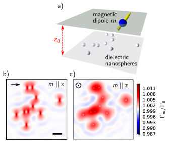
in equation (15) and then in expression (16). The results are presented in figure 3-b and c. When the particles are well-separated from each other, typically by one wavelength or more, they display a similar contrast as the one described in figure 2. This contrast is reinforced when several particles are grouped together. Isolated particles and assemblies of particles are surrounded by pseudoperiodic ripples that reveal the interferences between the emitting magnetic dipole and the sample.
IV Electric and magnetic dipole decay-rate close to complex dielectric nano-structures
Whereas equations (15) and (16) provide analytical expressions of the decay rate of magnetic dipoles placed close to very simple nano-objects, these equations can be complemented by an adequate discretization of the particle volume to describe light emission from dipoles in the vicinity of nanostructures of arbitrary geometries. To this end, we numerically implement the complete computation of the generalized propapagtor as described in reference Martin et al., 1995, together with (CGS unit), where defines the permittivity of the environment. We then use the propagator associated to the nanostructure with the mixed-field susceptibilities and in a discretized version of equation (15):
| (27) |
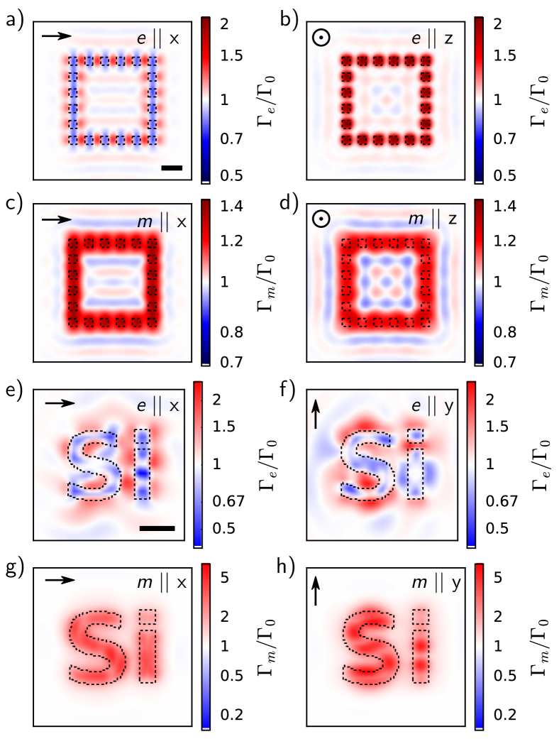
The sums (indexes and ) run over all discretization cells (of volume ) forming the nanostructure. This numerical procedure gives access to the optical response of complex systems, such as the ones described in figure 4. In this example, we have applied this technique to visualize the footprint induced by a perfect square corral composed of 20 dielectric structures in the initially flat ED and MD decay rate maps. The extension of the entire nanostructure is µm, the refractive index is . A modification of the decay rates ranging between 20 and 50 is obtained when the magnetic dipole is nm above the nanostructures (fig. 4c-d). Although the coupling is more efficient with an electric dipole (fig. 4a-b), especially when it is perpendicular, the coupling of the magnetic dipole with the dielectric structure remains quite significant and could be easily observed. In particular, the normalized contrast will be further enhanced when increasing from 2 to 4 or 5 using high optical index dielectric or semiconductor materials (TiO2, Si, or even Ge). To demonstrate this enhancement, we show in fig. 4e-h a flat silicon structure forming the letters “Si”, on which a magnetic decay rate enhancement of more than a factor can be observed. Moreover, we notice that the maps of the ED and MD decay rates display very specific features that will allow to discriminate unambiguously the electric or magnetic nature of the atomic transition. A similar identification method has been proposed and demonstrated using back-focal plane imaging of electric / magnetic dipole luminescence from rare-earth-doped films.Taminiau et al. (2012); Li et al. (2014) Our results suggest an alternative discrimination technique using nano-structured substrates, which could be performed on less complex optical detection schemes.
For instance, when the emitting dipole is oriented along the axis (maps (a), (c), (e) and (g) of figure 4), we observe a contrast reversal above the dielectric pads when passing from an electric to a magnetic dipole. This striking phenomenon is accompanied by a shift of the fringe pattern inside the corral by half a wavelength. Finally, another type of contrast change is observed when the dipole is perpendicular to the sample. In this second case, as illustrated by the maps (b) and (d) of figure 4, we move from a highly localized signal around the pads (map (b)) to a broader response distributed along the corral rows (map (d)).
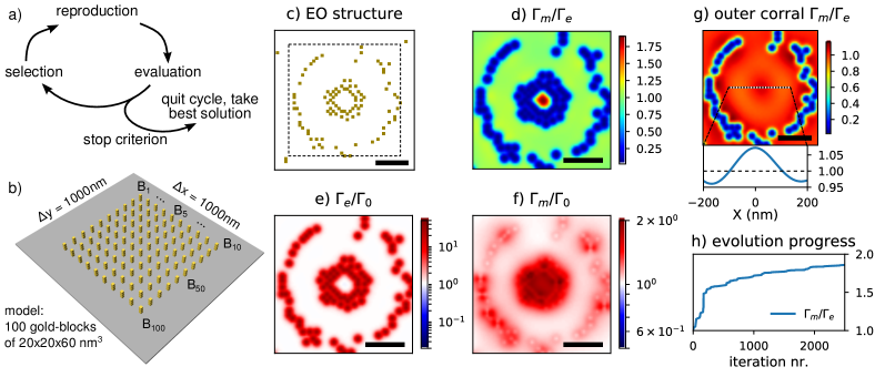
V Evolutionary optimization of metal nano-structures for maximum magnetic decay rate
In order to demonstrate the versatility of our model, we couple our numerical framework to an evolutionary optimization (EO) algorithm. EO tries to find optimum solutions to complex problems by mimicking the process of natural selection. Its principal idea is briefly depicted in figure 5a. Our approach to couple EO to numerical simulations is described in more detail in reference Wiecha et al., 2017. For technical information on the implementation and the used algorithm parameters, see the SI. In the supporting information, we also show an additional single- as well as a multi-objective evolutionary optimization problem, based on the decay-rate formalism. In this section, we use the permittivity of goldJohnson and Christy (1972) to demonstrate that our formalism is not limited to dielectric materials. The optimization goal is to find a gold nano-structure which maximizes the ratio of magnetic over electric decay rate at a fixed location ( nm). This is a particularly tricky scenario, because metals are known to have a far stronger response to electric dipole transitions than to magnetic ones. We use the evolutionary algorithm to optimize the geometry of a planar structure composed of gold pillars (each nm3), lying on a plane of nm2 (see figure 5b). We recall here that each subwavelength pillar does not support a direct magnetic response on its own. To render the positioning easier, the possible locations on the plane lie on a discretized grid (steps of nm). The structure is placed in vacuum and the wavelength is fixed at nm. We evolve a population of 150 individuals (nano-structures) over generations. Each of the individuals is a parameter-set consisting of positions for the 100 gold pillars, hence describing one possible structure. We tested the convergence by running the same optimization several times, reproducibly yielding similar structures and values for the decay rate ratio.
The optimum structure found by the EO algorithm is shown in figure 5c. Mappings of the decay rate ratio as well as the electric and magnetic decay rates are shown in figure 5d-g. Obviously, the algorithm succeeded in finding a gold nanostructure which significantly promotes magnetic decay at the target position (see Fig. 5d). This is particularly remarkable, because although gold structures easily provide very strong electric dipole decay rate enhancements, the magnetic LDOS is known to be usually very weak in metallic nanoparticles.Albella et al. (2013)
Two effects are being exploited by the optimized structure: The first mechanism is the different confinement of the decay rates for electric and magnetic dipoles close to material. The electric decay rate enhancement in the proximity of the gold pillars is high, but confined to a very small volume around the material. The magnetic decay rate on the other hand is more loosely enhanced around the gold clusters, leading to regions in their vicinity where is almost not affected, while still shows significant enhancement (c.f. figures 5e-f). The second effect is a modulation of the decay rate inside a larger resonator due to interference, similar to the corral shown in figures 1 and 4. At nm, the above presented corral had a maximum of in its center (see figure 4b and d). In contrast to this, the evolutionary algorithm distributed a fraction of the material (outer, circular structure) such, that is maximum in its center, which can be seen in figure 5g, where the decay rate has been calculated for the isolated outer structure.
We will conclude this section with some considerations on the convergence. One might wonder why the structure does not consist of perfect circles – this would very likely result in even better performance. Concerning this question, we have to keep in mind that possibilities exist to distribute the gold pillars on the available positions on the plane. Yet, the evolutionary algorithm did only evaluate different arrangements. Therefore, the reason why the material is not distributed on perfect circles is the heuristic nature of the evolutionary optimization algorithm. The search for the best structure did simply not converge to the very optimum. Comparing the optimized structure to an idealized version reveals, that the possible improvement in is only in the order of % (see also supporting information). We conclude that, despite the residual disorder in the geometry, the EO algorithm did converge very close to the ideal structure. Hence EO is a promising approach to this kind of problems.
VI Conclusions and Perspectives
In summary, we have developed a concise theoretical framework to describe the dynamics of light emission from magnetic dipoles located in complex nanostructured environments. This method, based on mixed field-susceptibilities, provides analytical expressions of the decay rate in the case of very simple environments. When the magnetic dipole is located close to nanostructures of arbitrary geometries, the computation of the MD decay rate involves the discretization of the nanostructure volume, the computation of a generalized propagator and finally the computation the decay rate from mixed field susceptibilities. This versatile framework is well suited to describe the emission of light from emitters involving both electric and magnetic dipole transitions as well as nano-optical processes comprising confined electric and magnetic fields. In addition, our framework is very flexible and can easily be extended. For instance nonlocality effects might be included by following the descriptions of Ref. Girard et al., 2015. Thanks to its computational simplicity, the method can also be employed within more complex numerical schemes. We demonstrated this possibility by coupling the magnetic decay rate calculation to an evolutionary optimization algorithm, which we employed to design a gold nanostructure for maximum contrast between magnetic and electric EM-LDOS. We also applied our method to the decay rate close to complex dielectric nanostructures. Our results suggest that it could be possible to identify the nature of the transition involved in the emission process (ED vs MD) from the variations of the decay rate in the vicinity of nanostructures. Finally, nanostructures possessing a particularly high contrast regarding dipole orientations could be designed using our evolutionary optimization.
Acknowledgements.
We thank Clément Majorel for his very useful contributions in the context of a Master’s training. This work was supported by Programme Investissements d’Avenir under the program ANR-11-IDEX-0002-02, reference ANR-10-LABX-0037-NEXT and by the computing facility center CALMIP of the University of Toulouse under grant P12167.References
- Novotny and Hecht (2006) L. Novotny and B. Hecht, Principles of Nano-Optics (Cambridge University Press, Cambridge ; New York, 2006).
- Anger et al. (2006) P. Anger, P. Bharadwaj, and L. Novotny, Physical Review Letters 96, 113002 (2006).
- Kühn et al. (2006) S. Kühn, U. Håkanson, L. Rogobete, and V. Sandoghdar, Physical Review Letters 97, 017402 (2006).
- Kinkhabwala et al. (2009) A. Kinkhabwala, Z. Yu, S. Fan, Y. Avlasevich, K. Müllen, and W. E. Moerner, Nature Photonics 3, 654 (2009).
- Curto et al. (2010) A. G. Curto, G. Volpe, T. H. Taminiau, M. P. Kreuzer, R. Quidant, and N. F. van Hulst, Science 329, 930 (2010).
- Biagioni et al. (2012) P. Biagioni, J.-S. Huang, and B. Hecht, Reports on Progress in Physics 75, 024402 (2012).
- Novotny and van Hulst (2011) L. Novotny and N. van Hulst, Nature Photonics 5, 83 (2011).
- Klimov et al. (1996) V. V. Klimov, M. Ducloy, and V. S. Letokhov, Journal of Modern Optics 43, 2251 (1996).
- Giessen and Vogelgesang (2009) H. Giessen and R. Vogelgesang, Science 326, 529 (2009).
- Aigouy et al. (2014) L. Aigouy, A. Cazé, P. Gredin, M. Mortier, and R. Carminati, Physical Review Letters 113, 076101 (2014).
- Choi et al. (2016) B. Choi, M. Iwanaga, Y. Sugimoto, K. Sakoda, and H. T. Miyazaki, Nano Letters 16, 5191 (2016).
- Karaveli and Zia (2011) S. Karaveli and R. Zia, Physical Review Letters 106, 193004 (2011).
- Carminati et al. (2015) R. Carminati, A. Cazé, D. Cao, F. Peragut, V. Krachmalnicoff, R. Pierrat, and Y. De Wilde, Surface Science Reports 70, 1 (2015).
- Baranov et al. (2017) D. G. Baranov, R. S. Savelev, S. V. Li, A. E. Krasnok, and A. Alù, Laser & Photonics Reviews 11, 1600268 (2017).
- Cuche et al. (2017) A. Cuche, M. Berthel, U. Kumar, G. Colas des Francs, S. Huant, E. Dujardin, C. Girard, and A. Drezet, Physical Review B 95, 121402 (2017).
- Purcell et al. (1946) E. M. Purcell, H. C. Torrey, and R. V. Pound, Physical Review 69, 37 (1946).
- Chicanne et al. (2002) C. Chicanne, T. David, R. Quidant, J. C. Weeber, Y. Lacroute, E. Bourillot, A. Dereux, G. Colas des Francs, and C. Girard, Physical Review Letters 88, 097402 (2002).
- Rolly et al. (2012) B. Rolly, B. Bebey, S. Bidault, B. Stout, and N. Bonod, Physical Review B 85, 245432 (2012).
- Chigrin et al. (2016) D. N. Chigrin, D. Kumar, D. Cuma, and G. von Plessen, ACS Photonics 3, 27 (2016).
- Chew (1979) H. Chew, Physical Review A 19, 2137 (1979).
- Klimov and Letokhov (2005) V. V. Klimov and V. S. Letokhov, Laser physics 15, 61 (2005).
- Schmidt et al. (2012) M. K. Schmidt, R. Esteban, J. J. Sáenz, I. Suárez-Lacalle, S. Mackowski, and J. Aizpurua, Optics Express 20, 13636 (2012).
- Stout et al. (2011) B. Stout, A. Devilez, B. Rolly, and N. Bonod, JOSA B 28, 1213 (2011).
- Feng et al. (2011) T. Feng, Y. Zhou, D. Liu, and J. Li, Optics Letters 36, 2369 (2011).
- Hein and Giessen (2013) S. M. Hein and H. Giessen, Physical Review Letters 111, 026803 (2013).
- Albella et al. (2013) P. Albella, M. A. Poyli, M. K. Schmidt, S. A. Maier, F. Moreno, J. J. Sáenz, and J. Aizpurua, The Journal of Physical Chemistry C 117, 13573 (2013).
- Mivelle et al. (2015) M. Mivelle, T. Grosjean, G. W. Burr, U. C. Fischer, and M. F. Garcia-Parajo, ACS Photonics 2, 1071 (2015).
- Feng et al. (2016) T. Feng, Y. Xu, Z. Liang, and W. Zhang, Optics Letters 41, 5011 (2016).
- Burresi et al. (2009) M. Burresi, D. van Oosten, T. Kampfrath, H. Schoenmaker, R. Heideman, A. Leinse, and L. Kuipers, Science 326, 550 (2009).
- Devaux et al. (2000a) E. Devaux, A. Dereux, E. Bourillot, J.-C. Weeber, Y. Lacroute, J.-P. Goudonnet, and C. Girard, Applied Surface Science 164, 124 (2000a).
- Devaux et al. (2000b) E. Devaux, A. Dereux, E. Bourillot, J.-C. Weeber, Y. Lacroute, J.-P. Goudonnet, and C. Girard, Physical Review B 62, 10504 (2000b).
- Girard et al. (1997) C. Girard, J.-C. Weeber, A. Dereux, O. J. F. Martin, and J.-P. Goudonnet, Physical Review B 55, 16487 (1997).
- Schröter (2003) U. Schröter, The European Physical Journal B 33, 297 (2003).
- Martin et al. (1995) O. J. F. Martin, C. Girard, and A. Dereux, Physical Review Letters 74, 526 (1995).
- Girard (2005) C. Girard, Reports on Progress in Physics 68, 1883 (2005).
- Agarwal (1975) G. S. Agarwal, Physical Review A 11, 230 (1975).
- Sersic et al. (2011) I. Sersic, C. Tuambilangana, T. Kampfrath, and A. F. Koenderink, Physical Review B 83, 245102 (2011).
- Kwadrin and Koenderink (2013) A. Kwadrin and A. F. Koenderink, Physical Review B 87, 125123 (2013).
- Lunnemann and Koenderink (2016) P. Lunnemann and A. F. Koenderink, Scientific Reports 6, srep20655 (2016).
- Pendry (2000) J. B. Pendry, Physical Review Letters 85, 3966 (2000).
- Soukoulis et al. (2007) C. M. Soukoulis, S. Linden, and M. Wegener, Science 315, 47 (2007).
- Arbouet et al. (2014) A. Arbouet, A. Mlayah, C. Girard, and G. Colas des Francs, New Journal of Physics 16, 113012 (2014).
- Bakker et al. (2015) R. M. Bakker, D. Permyakov, Y. F. Yu, D. Markovich, R. Paniagua-Domínguez, L. Gonzaga, A. Samusev, Y. Kivshar, B. Luk’yanchuk, and A. I. Kuznetsov, Nano Letters 15, 2137 (2015).
- Decker and Staude (2016) M. Decker and I. Staude, Journal of Optics 18, 103001 (2016).
- Kuznetsov et al. (2016) A. I. Kuznetsov, A. E. Miroshnichenko, M. L. Brongersma, Y. S. Kivshar, and B. Luk’yanchuk, Science 354 (2016), 10.1126/science.aag2472.
- Taminiau et al. (2012) T. H. Taminiau, S. Karaveli, N. F. van Hulst, and R. Zia, Nature Communications 3, ncomms1984 (2012).
- Li et al. (2014) D. Li, M. Jiang, S. Cueff, C. M. Dodson, S. Karaveli, and R. Zia, Physical Review B 89, 161409 (2014).
- Wiecha et al. (2017) P. R. Wiecha, A. Arbouet, C. Girard, A. Lecestre, G. Larrieu, and V. Paillard, Nature Nanotechnology 12, 163 (2017).
- Johnson and Christy (1972) P. B. Johnson and R. W. Christy, Physical Review B 6, 4370 (1972).
- Girard et al. (2015) C. Girard, A. Cuche, E. Dujardin, A. Arbouet, and A. Mlayah, Optics Letters 40, 2116 (2015).