Effect of plasma formation on the double pulse laser excitation of cubic silicon carbide
Abstract
We calculate the electron excitation in cubic silicon carbide (3C-SiC) caused by the intense femtosecond laser double pulses using time-dependent density functional theory (TDDFT). We assume the electron distributions in the valence band (VB) and the conduction band (CB) based on three different approaches to determine the dependence of the plasma that is formed on the excitation by the first pulse. First, we consider the simple double pulse irradiation, which does not include the electron-electron collisions and relaxation. Second, we consider the partially thermalized electronic state, in which the electron temperatures and numbers in the VB and the CB are defined independently. This assumption corresponds to the plasma before the electron-hole collisions becomes dominant. The third approach uses the fully thermalized electron distribution, which corresponds to a timescale of hundreds fs. Our results indicate that the simple double pulse approach is the worst of the three, and show that the plasma formation changes the efficiency of the excitation by the second pulse. When the electron temperature decreases, the laser excitation efficiency increases as a result.
Processing of solid materials using femtosecond laser pulses has attracted considerable interest for potential application to high-precision processing technology. Chichkov ; Stuart ; Liu ; Lenzner ; Geissler ; Lenzner00 ; Sudrie ; Doumy ; Amoruso ; Gattass08 ; Reif10 ; Gamaly11 ; Chimier Because a femtosecond laser pulse can deposits large amounts of energy into solid materials within a much shorter time than conventional spatial diffusion of thermal energy to the exterior of the irradiated spot, we can process materials with small thermal denaturation outside of the irradiated volume.Gattass08 ; Reif10 ; Gamaly11
The peak intensity of a femtosecond laser pulse can be very high when compared with that of longer laser pulses and is thus suitable for processing of wide gap materials and dielectrics by nonlinear processes. However, the high peak laser intensity laser sometimes induces the damage in optical elements, such as lenses, gratings, and mirrors. Therefore, the laser processing efficiency at the peak laser intensity is important.
Recently, double-pulse irradiation has been proposed as a new approach for efficient laser processing Shi14 ; Sandra15 ; Sandra15-2 ; Furukawa16 . We found that the double- or multi-pulse irradiation reduces the ablation threshold intensity in SiC Hayashi16 ; Hayashi16-2 . Because the timescales of the fast electron-electron and hole-hole relaxation are of the order of 100 fs, and the carrier relaxation time is of the order of hundreds fs Michael17 , features of the formed plasma are also important in multi-pulse processing.
In this work, we simulate the electron excitation processes in the 3C-SiC caused by the double femtosecond laser pulses using the time-dependent density functional theory (TDDFT) with a real-time real-space approach Runge84 ; Bertsch00 ; Otobe08 . SiC is one of the important material as a foundation base in the next generation, because of its wide bandgap ( eV), temperature resistance, good thermal conductivity as well as impact resistance Morkoc94 ; Matsunami98 . However, for its hardness and chemical, mechanical stability, SiC is difficult to be processed. Therefore, efficient processing of SiC by femtosecond laser pulses will be an important technique Choi16 .
To explain the effect of the relaxation process, we assume that the thermalized electron and hole states in the conduction and the valence bands can be expressed by using some Fermi distribution functions. We assume the one temperature for all electronic states Sato15 and individual two temperatures for the conduction and the valence band. The first assumption corresponds to a timescale of ps, and the second assumption corresponds to a timescale of few tens to hundreds of fs.
In real-time TDDFT, we describe the electron dynamics in a unit cell of a crystalline solid under a spatially uniform electric field . By treating the field using a vector potential, we obtained . We assumed that the laser was linearly polarized, and that the polarization direction was parallel to the axis. The electron dynamics were described by the time-dependent Kohn-Sham (TDKS) equation Runge84 , which is a fundamental equation of TDDFT. Real-time calculations were performed using the SALMON (Scalable Ab-inito simulator for Light-Matter interactions in Optics and Nanoscience) program packageSALMON . We modified SALMON to treating the temperatures of the valence and the conduction bands individually. In this work, we used the modified Becke-Johnson (mBJ) exchange potential mBJ ; mBJ2 given as Eqs. (2)-(4) in Ref. mBJ2 with a local-density approximation (LDA) correlation potential LDA under an adiabatic approximation. The -value in the mBJ potential was set at 1.35 to reproduce the optical band gap of 3C-SiC (6eV).
A cubic unit cell containing four silicon atoms and four carbon atoms was discretized into Cartesian grids containing points. The space was also discretized into grid points. We used a time step of 0.04 a.u.
The laser electric field was assumed to be
| (1) |
where is the maximum electric field amplitude and is the center of the laser frequency ( eV). is related to the incident laser field () by , where is the dielectric function at yabana12 . The pulse length was set at six optical cycles (16.2 fs), and the polarization was parallel to the [0,0,1] direction.
We used the LDA functional to calculate the time-dependent total energy, , because the mBJ potential does not have an energy functional. The absorbed energy is defined as the difference of the between the initial and final values of , where .
The hole density is defined by the projection of the time-dependent wavefunction at () onto the initial state given by , where and are the band indices of the orbitals for the initial and time-dependent states, respectively, and is the wavefunction of the initial state for which the Bloch wave vector is shifted by the laser field . Otobe08
Individual projections to the initial states given by , give the occupation of state . We prepare adequate unoccupied states in the conduction band, typically comprising 100 states for each , to calculate the overall electron distribution. The reduced internal energies in the conduction and valence bands, given by and , respectively, can be defined as
| (2) |
where represents states in the valence (conduction) band, and is the energy eigenvalue of the -th state.
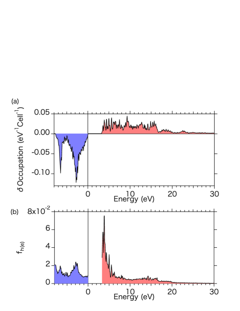
Figure 2 (a) shows the change in the electron distribution, , in the form of the density of states (DoS) for the case of a laser intensity of W/cm2. A broad distribution in the conduction band and specific peaks in the valence band are shown. The hole (electron) filling rate, , is also shown in Fig. 2 (b).
Three possible assumptions can be used to reproduce the electron distribution after the laser pulse ends. First, the collisional process is assumed to be negligible and the electron and hole distributions remain unchanged until the second pulse arrives. Second, the electrons and holes are assumed to relax in each of the bands, and the distribution is thermalized. In general, the electron-electron collision time in the same band is shorter than the corresponding time between the valence and the conduction bands Michael17 . Therefore, this assumption may corresponds to the transient state leading to true thermalization. Third, the whole system is assumed to be thermalized and the electron distribution can then be expressed using a single temperature, the corresponds to a much longer time delay than the second assumption.
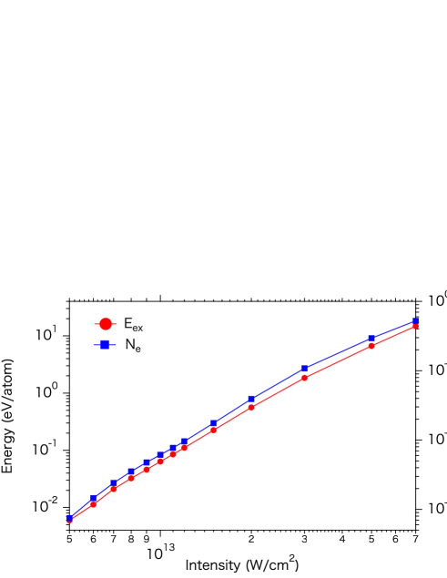
In the second assumption, we can define the distribution function to reproduce at a fixed . In this fitting, both the chemical potential and the electron temperature in each of the bands are treated as parameter. Figure 3 (a) shows the laser intensity dependence of and . The figure shows a nonlinearly increase in temperature in the conduction band above W/cm2. The black dashed line represents the Keldysh parameter (), which serves as an index for the multiphoton and tunneling excitation processes. The multiphoton process is dominant when , while the tunneling process is dominant when . acrosses 1 at an intensity of W/cm2. Therefore the tunneling process increases the conduction band temperature and the temperatures of the valence and conduction bands becomes closer.
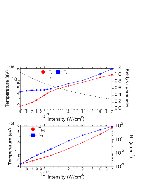
Figure 3 (b) shows the fitted electron temperature in all bands () to reproduce , which corresponds to the third assumption. In this fitting, we define the single electron temperature. Therefore, the number of the excited electrons cannot by fixed artificially. The calculated number of excited electrons () is also plotted using blue squares. is approximately twice of at all intensities. The figure shows a small kink at an intensity of W/cm2 that corresponds to the tunneling regime, where .
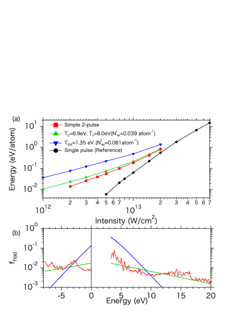
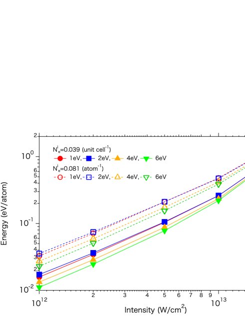
In the next step, we simulated the double pulse excitation. We assumed that the intensity of the first pulse is W/cm2. The absorbed energy at an intensity of W/cm2 is 0.56 eV/atom, which is much lower than the cohesive energy of 6.34 eV/atom Jiang16 ; Chang87 and higher than the melting point energy of eV/atom Sace60 ; Handbook . Therefore, ultrafast deformation related to ablation may not occur Sato15 . We confirmed that the is 6.9 eV, and is 8.0 eV in the second assumption. In the third assumption, the electron temperature and are defined as eV and atom-1, respectively.
Figure 4 (a) shows the energy absorbed from the second pulse, . For reference, absorbed from the single pulse is plotted using black circles. The parameters of the second laser pulse are same as those of the first pulse. In the first assumption (red squares), the time delay between the two pulses was set at 19 fs.
In all cases, is higher than the energy from the single pulse calculations, and shows a linear dependence on laser intensity. This result indicates that photoabsorption by the plasma is important. In particular, the efficiency is very high in the case where the temperature is fixed at eV (part of the third assumption). In this case, the excited electron density is twice that of the other cases, (0.081 atom-1), which may be the reason why this case is the most efficient.
While is the same in the other two cases, we can also see significant differences between them. The simple two-pulse simulation (red squares) shows the worst results, and the two-temperature assumption (green triangles) shows better results. The differences among these three cases involve the distributions of the electrons and holes when the second pulse irradiates the surface. The filling rate, , before the second pulse begins is shown in Fig. 4 (b). A higher electron (hole) concentration at the bottom (top) of the conduction (valence) band produces a higher . In particular, the simple double pulse case shows a non-monotonic distribution. In other words, the electron excitation by the second pulse is dependent on the features of the prepared plasma.
To describe the electron temperature dependence of the electron excitation by the second pulse, we calculated the using different initial numbers of excited electrons () and the temperatures. We define the electron temperature as , to simplify the assumption. Figure 5 shows the dependence of on and . The efficiency increases as decreases in both cases of , and is highest at eV.
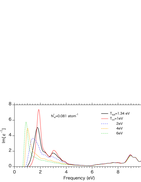
One possible reason why is dependent on and is its dependence on the formed plasma. The most convenient way to show the plasma contribution to the response is to plot the imaginary part of the inverse dielectric function Im[] Figure 6 shows the Im[] for various temperature at a fixed atom-1. The plasmon peak shifts from 0.8 to 2 eV as the decreases. According to the simple Drude model, the plasma frequency is dependent on where is the effective electron mass. Therefore, our results indicate that the effective mass increases as the increases, which is consistent with the prior work of Sato et al Sato14 . Electrons and holes on higher energy states have heavy effective masses and this causes a lower plasma frequency.
From first-principles simulations, we conclude that the efficiency of the laser excitation using double pulses is dependent on the features of the plasma formed by the first pulse. A higher excited electron density at a lower temperature is preferred because the lower temperature produces a higher plasma frequency. While this condition appears to be conflicting in wide-gap semiconductors and insulators, it may be possible to produce it using laser pulse tuned to the optical band gap or phonon-assisted excitation of the band edge by the first pulse.
Acknowledgement
This work was supported by JSPS KAKENHI (Grants Nos. 15H03674 and 17K05089) and CREST (JST Grant No. JPMJCR16N5). Numerical calculations were performed on the SGI ICE X supercomputer at the Japan Atomic Energy Agency (JAEA).
References
- (1) B. N. Chichkov, C. Momma, S. Nolte, V. von Alvensleben, and A. Tunnermann, Appl. Phys. A 63, 109 (1996).
- (2) B. C. Stuart, M. D. Feit, S. Herman, A. M. Rubenchik, B. W. Shore, and M. D. Perry, Phys. Rev. B 53, 1749 (1996).
- (3) X. Liu, D. Du, and G. Mourou, IEEE J. Quantum Electron. 33, 1706 (1997).
- (4) M. Lenzner, J. Kröger, S. Sartania, Z. Cheng, Ch. Spielmann, G. Mourou,W. Kautek, and F. Krausz, Phys. Rev. Lett. 80, 4076 (1998).
- (5) M. Geissler, G. Tempea, A. Scrinzi, M. Schnürer, F. Krausz, and T. Brabec, Phys. Rev. Lett. 83, 2930 (1999).
- (6) M. Lenzner, F. Krausz, J. Krüger, and W. Kautek, Appl. Surf. Sci. 154, 11 (2000).
- (7) L. Sudrie, A. Couairon, M. Franco, B. Lamouroux, B. Prade, S. Tzortzakis, and A. Mysyrowicz, Phys. Rev. B 89, 186601 (2002).
- (8) G. Doumy, F. Quéré, O. Gobert, M. Perdrix, Ph. Martin, P. Audebert, J. C. Gauthier, J.-P. Geindre, and T. Wittmann, Phys. Rev. E 69, 026402 (2004).
- (9) S. Amoruso, G. Ausanio, R. Bruzzese, M. Vitiello, and X. Wang, Phys. Rev B 71, 033406 (2005).
- (10) R. R. Gattass and E. Mazur, Nat. Photonics 2, 219 (2008).
- (11) J. Reif, in Laser-Surface Interaction for New Materials Production, edited by A. Miotello and P. M. Ossi (Springer, Berlin, 2010).
- (12) E. G. Gamaly, Phys. Rep. 508, 91 (2011).
- (13) B. Chimier, O. Utéza, N. Sanner, M. Sentis, T. Itina, P. Lassonde, F. Legare, F. Vidal, and J. C. Kieffer, Phys. Rev. B 84, 094104 (2011)
- (14) X. Shi, L. Jiang, X. Li, K. Zhang, D. Yu, Y. Yu, and Y. Lu, J. Appli. Phys. 116, 033104 (2014).
- (15) S. Höhm, M. Herlieb, A. Rosenfeld, J. Krüger, and J. Bonse, Opt. Exp. 23, 000061 (2015).
- (16) S. Höhm, M. Herlieb, A. Rosenfeld, J. Krüger, and J. Bonse, Opt. Exp. 23, 025959 (2015).
- (17) Y. Furukawa, R. Sakata, K. Konishi, K. Ono, S. Matsuoka, K. Watanabe, S. Inoue, M. Hashida, and S. Sakabe, Appli. Phys. Lett. 108, 264101 (2016).
- (18) Terutake Hayashi, et al, Proceedings of JSPE Semestrial Meeting 2016A, 221-222 (2016).
- (19) K. Matsunaga, H. Hayashi, S. Kurokawa, H. Yokoo, N. Hasegawa, M. Nishikino, T. Kumada, T. Otobe, Y. Matsukawa, Y. Takaya, Proceedings of the 15th International Conference on X-ray Lasers, Springer Proceedings in Physics (in Press.).
- (20) Michael Zurch, et al, Nat. Comm. 8, 15734 (2017).
- (21) E. Runge and E. K. U. Gross, Phys.Rev. Lett. 52, 997 (1984).
- (22) G.F. Bertsch, J.-I. Iwata, A. Rubio, and K. Yabana, Phys. Rev. B 62 , 7998 (2000).
- (23) T. Otobe, M. Yamagiwa, J. -I. Iwata, K. Yabana, T. Nakatsukasa, and G. F. Bertsch, Phys. Rev. B77, 165104 (2008).
- (24) H. Morkoc, et al, J. Appli. Phys. 76, 1363 (1994).
- (25) H. Matsunami and T. Kimoto, Mat. Sci. Eng. R. 20, 125 (1998)
- (26) I. Choi, et al, Nat. Comm. 7, 13562 (2016).
- (27) S. A. Sato, K. Yabana, Y. Shinohara, T. Otobe,K.-M. Lee, and G.F. Bertsch, Phys. Rev. B 92 205413 (2015).
- (28) A. D. Becke and E. R. Johnson, J. Chem. Phys. 124 221101 (2006).
- (29) F. Tran and P. Blaha, Phys. Rev. Lett. 102, 226401 (2009).
- (30) J. P. Perdew and Y. Wang, Phys. Rev. B 45, 13244 (1992).
- (31) K. Yabana, T. Sugiyama, Y. Shinohara, T. Otobe, and G. F. Bertsch, Phys. Rev. B 85, 045134 (2012). http://salmon-tddft.jp/wiki/Main_Page
- (32) K. Yabana, T. Sugiyama, Y. Shinohara, T. Otobe, and G. F. Bertsch, Phys. Rev. B 85, 045134 (2012).
- (33) L.V. Keldysh, Sov. Phys. JETP 20, 1307 (1965).
- (34) S. A. Sato, K. Yabana, Y. Shinohara, T. Otobe, G.F. Bertsch, Phys. Rev. B 89, 064304 (2014).
- (35) M. Jiang, S. M. Peng, H. B. Zhang, C. H. Xu, H. Y. Xiao, F. A. Zhao, Z. J. Lio, and X. T. Zu, Sci. Rep. 6, 20669 (2016).
- (36) K. J. Chang and M. L. Cohen, Phys, Rev. B 35, 8196 (1987).
- (37) R. I. Sace and G. A. Slack, in Silicon Carbide-A high temperature Semiconductor, edited by J. R. O’connor, J. Smiltens (Pregamon Press, Oxford, London, New York, Paris, 1960).
- (38) CRC Material Science Engineering Handbook, edited by James F. Shackelfold, and William Alexander, (CRC Press LLC, Boca Raton, London, New York, Washinton, D. C., 2001)