Probing low noise at the MOS interface with a spin-orbit qubit
I Introduction
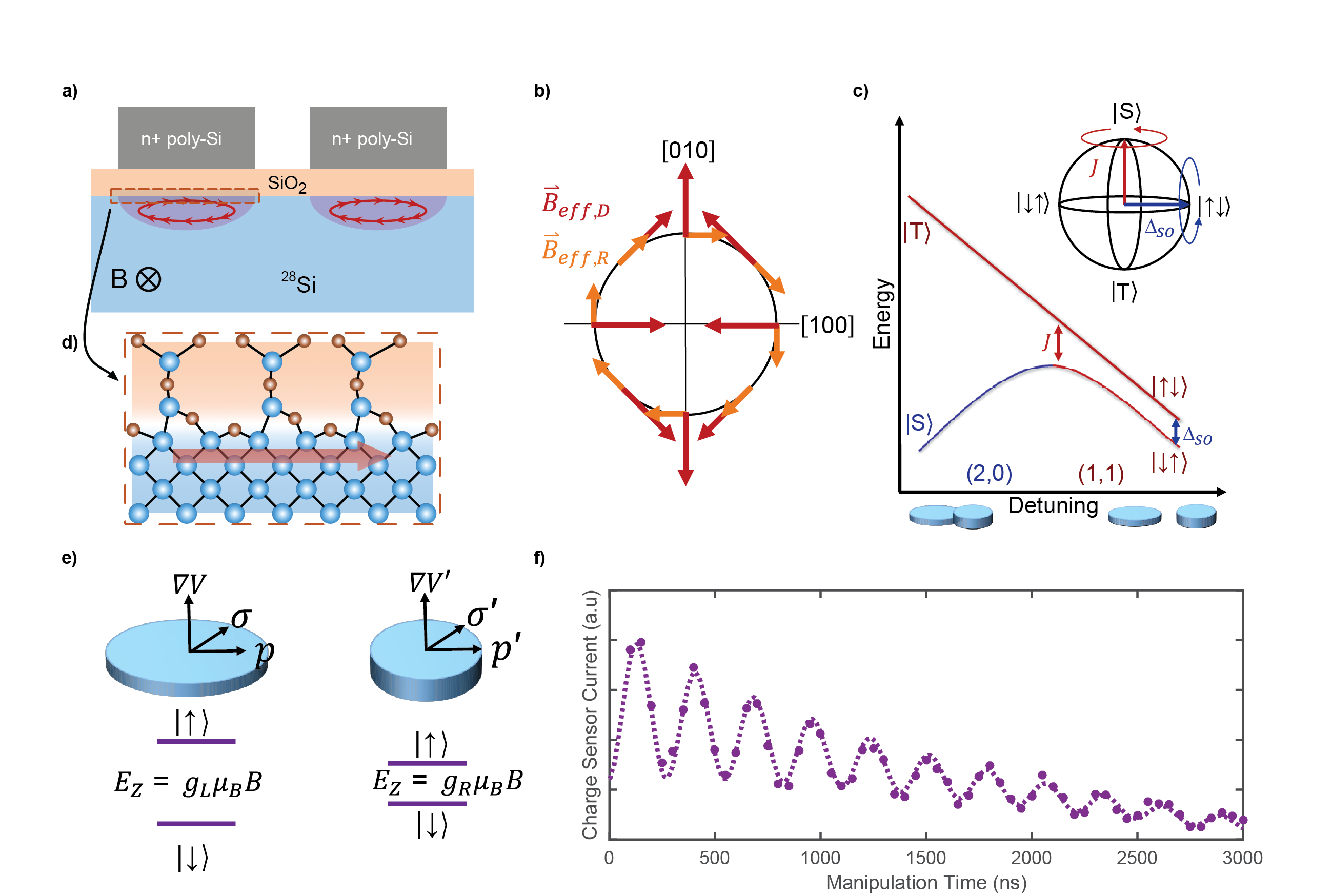
The silicon metal-oxide-semiconductor (MOS) material system is technologically important for the implementation of electron spin-based quantum information technologies. Researchers predict the need for an integrated platform in order to implement useful computation Vandersypen et al. (2016), and decades of advancements in silicon microelectronics fabrication lends itself to this challenge. However, fundamental concerns have been raised about the MOS interface (e.g. trap noise, variations in electron g-factor and practical implementation of multi-QDs). Furthermore, two-axis control of silicon qubits has, to date, required the integration of non-ideal components (e.g. microwave strip-lines, micro-magnets, triple quantum dots, or introduction of donor atoms). In this paper, we introduce a spin-orbit (SO) driven singlet-triplet (ST) qubit in silicon, demonstrating all-electrical two-axis control that requires no additional integrated elements and exhibits charge noise properties equivalent to other more model, but less commercially mature, semiconductor systems Petersson et al. (2010); Shi et al. (2013); Dial et al. (2013); Wu et al. (2014). We demonstrate the ability to tune an intrinsic spin-orbit interface effect, which is consistent with Rashba and Dresselhaus contributions that are remarkably strong for a low spin-orbit material such as silicon. The qubit maintains the advantages of using isotopically enriched silicon for producing a quiet magnetic environment, measuring spin dephasing times of 1.6 using 99.95% 28Si epitaxy for the qubit, comparable to results from other isotopically enhanced silicon ST qubit systems Harvey-Collard et al. (2015); Eng et al. (2015); Rudolph et al. (2017). This work, therefore, demonstrates that the interface inherently provides properties for two-axis control, and the technologically important MOS interface does not add additional detrimental qubit noise.
Creating qubits using the silicon metal-oxide-semiconductor (MOS) material system is compelling because of its quiet nuclear environment and the future promise of building upon CMOS capability. Recently, several critical demonstrations for qubit viability in MOS quantum dots (QDs) have been made including: (1) large tunable valley-splitting reproduced in multiple process flows Gamble et al. (2016), (2) long spin coherence times Veldhorst et al. (2014), and (3) fast coherent exchange coupling of spins in a multi-quantum dot layout Veldhorst et al. (2015a). Yet, the intrinsically imperfect Si/SiO2 interface produces persistent central concerns about charge traps and uncertainty in the degree to which the electron -factor may be controlled Veldhorst et al. (2014). In particular, charge traps and two-level fluctuators near the interface are believed to be potential sources of noise in MOS devicesRalls et al. (1984); Culcer and Zimmerman (2013). The prevailing material choice for Si qubits is heteroepitaxial Si/SiGe, which shifts the imperfect crystal-dielectric interface further away. However, there are doubts about reproducible valley splitting Borselli et al. (2011) in this system, and the qubit structures diverge from conventional CMOS design. No direct measurement of charge noise at the MOS interface has been made, though indirect measures on spin qubits Veldhorst et al. (2015a); Harvey-Collard et al. (2015); Rudolph et al. (2017) suggest the effect will not impede coherent control. Variability in -factor has also been observed, introducing complications in qubit device architecture Jones et al. (2016). Recent work has attributed variability in electron -factor at silicon interfaces to spin-orbit coupling and interface disorder, including step edges Veldhorst et al. (2014, 2015b); Ferdous et al. (2017a, b). Spin-orbit coupling effects have been studied extensively in III-V quantum dot systems Pfund et al. (2007); Fasth et al. (2007); Nadj-Perge et al. (2010a, b); Stepanenko et al. (2012); Rančić and Burkard (2014); Scarlino et al. (2014); Nichol et al. (2015). However, these effects have not, to date, been fully understood in the MOS material system. The results in this paper address both of these fundamental doubts about the MOS interface by showing that: (1) the spin-orbit interaction can be either turned off or tuned as a useful quantity, and (2) the charge noise at the MOS interface is comparable to other qubit systems.
In bulk Si, the SO interaction leads to only weakly perturbed -factors that are close to . However, the inversion asymmetry of the crystal at an interface leads to a SO interactionRössler and Kainz (2002); Golub and Ivchenko (2004); Nestoklon et al. (2006); Prada et al. (2011), as shown in Fig. 1. When a magnetic field is applied with a component parallel to the interface, electron cyclotron motion establishes a non-zero net momentum component along the interface, Fig. 1(a). The coupling of the electron momentum perpendicular to the effective electric field at the interface produces the SO interaction. The asymmetry of the electric potential at the interface leads to a Rashba SO contribution due to structural inversion asymmetry (SIA). A second interaction, the Dresselhaus contribution, is attributed to microscopic interface inversion asymmetry (IIA)Nestoklon et al. (2008). The Rashba and Dresselhaus SO couplings for an electron confined to an interface have the form and , respectively, where and are the relative coupling strengths. The operators , are Pauli spin matrices, while , are components of the kinetic momentum along the , direction, with the elementary unit of charge and the vector potential. This work quantitatively and unambiguously characterizes the SO effect at the MOS interface over its full angular dependence and provides a theoretical framework that removes the gauge-dependent ambiguity of previous models of interface Rashba-Dresselhaus coupling. We note that this interface effect is not theoretically unique to Si interfaces Rössler and Kainz (2002); Golub and Ivchenko (2004); Alekseev and Nestoklon (2017). Because of its strength and angular dependence that is similar to bulk SO effects, it is possible that the contribution of the interface effect, particularly on the Dresselhaus coupling, is under-appreciated in other systems that leverage strong SO coupling. Improved understanding of this effect has the potential to influence areas such as spintronics and the pursuit of forming new topological states of matter Manchon et al. (2015); Soumyanarayanan et al. (2015).
II Results
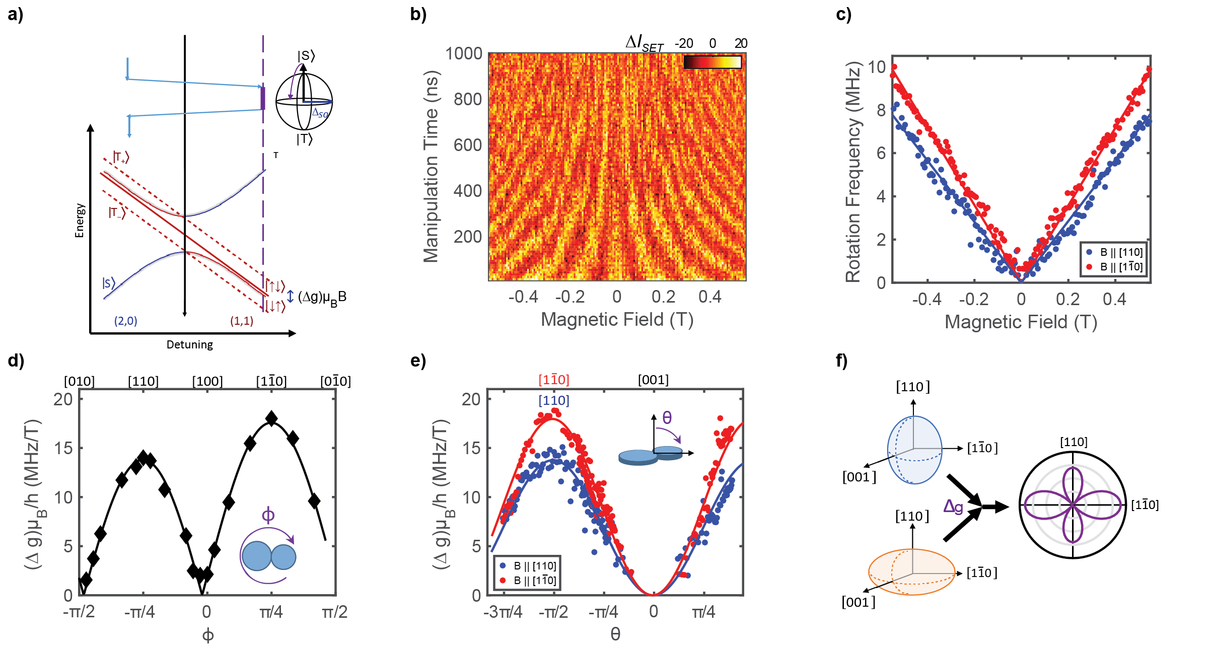
The qubit in this work is formed within a MOS double quantum dot (DQD). Two electrons are electrostatically confined within a double well potential, where the dominant interaction between the electrons can be electrically tuned between two regimes for two-axis control, Fig. 1(c). When the electronic wave functions of the QDs overlap significantly, the exchange energy, , dominates. When the two electrons are well separated, is small and distinct Zeeman Hamiltonians result from the differences in their interface SO coupling. The difference in SO coupling leads to a variation in effective electron -factors, Fig. 1(e), and amounts to an effective magnetic field gradient between the QDs that can be tuned with control of the applied electric and magnetic fields. Thus, we achieve all-electrical two-axis control using native features of the MOS DQD system, avoiding the substantial fabrication complications of other Si qubit schemes.
We define the computational basis as the eigenstates of the two-spin system in the limit of a large singlet-triplet exchange energy, . Specifically, these are the two states, and , of the subspace, which form a decoherence-free subspace relative to fluctuations in a uniform B-field Lidar et al. (1998). An applied magnetic field splits the spin triplet states () and states by the Zeeman energy to isolate the subspace. A qubit state can then be initialized in a singlet ground state when the two QDs are electrically detuned out of resonance such that it is preferable to have a charge state, Fig 1(c). Rapid adiabatic passage to the charge state produces a superposition of the stationary eigenstates in the gradient field. A difference in the Larmor spin precession frequency of the two QDs induces -rotations between the and states, Fig. 1(f) and 2(a). For each QD the angular precession frequency is given by , where is the electron -factor, is the Bohr magneton, is Planck’s constant, and is the applied magnetic field. The two-electron spin qubit will oscillate between the and states at a frequency . -rotations can be turned on by shifting the detuning closer to the charge anti-crossing where is larger, driving oscillations around the equator of the Bloch sphere, Fig 1(c). The spin state is detected using Pauli blockade, combined with a remote charge sensor that detects whether the qubit state passed through the charge state or was blockaded in during the readout stageHarvey-Collard et al. (2017).
The spin splitting of an electron in a QD is governed by an effective Zeeman Hamiltonian of the form , where is the magnetic field vector, is the vector of Pauli spin matrices and is the electron -tensor. Including the and SO Hamiltonians perturbatively leads to an effective -tensor of the form
| (1) |
The strength of the SO interaction is predicted to depend on applied electric field, lateral confinement, valley-orbit configuration, and the atomic-scale structure of the interface (see supplementary material). Consequently, the local interfacial and electrostatic environments particular to each QD produce differences in effective -tensor, Fig. 2(f). This will act as a difference in effective in-plane magnetic field, modifying the electron spin splitting between dots and drive rotations at a frequency
| (2) |
where is the field direction in-plane of the interface with respect to the crystallographic direction and is the out-of-plane angle relative to .
In Fig. 2(b), we show the singlet return signal as a function of time spent at the manipulation point in as the external magnetic field is varied along the crystallographic direction. The observed oscillations demonstrate the ability to control coherent rotations. The rotation frequency displays a clear magnetic field dependence. In Fig. 2(c), we plot the SO-induced rotation frequency as a function of field for both the and directions. The linear dependence on field is consistent with a -factor difference between the two QDs (), whereas the difference in the slopes indicates an angular dependence for . We plot the full angular dependence of the SO interaction in Figs. 2(d) and 2(e). Figure 2(d) shows the measured difference in gyromagnetic ratio between the dots, , as a function of the in-plane angle relative to the [100] crystallographic direction. Dependence on the out-of-plane angle, , is shown in Fig. 2(e). Here, is fixed along the [110] ([10]) direction and the measured difference in gyromagnetic ratio between the dots is plotted in blue (red) as the field is tilted out of the interface plane ( = 0 is along the direction). Qualitatively, the angular dependence is consistent with a SO effect, slightly different in each QD, composed of Rashba and Dresselhaus contributions. Enhanced interface SO effects in Si have been surmised previously for in-plane B-field dependencesYang et al. (2013); Tahan and Joynt (2014); Hwang et al. (2017). We plot fits to equation (2) along with the data in Figs. 2(d) and 2(e). We extract relative SO parameters = 1.89 MHz/T and = 15.7 MHz/T. The maximum useful B-field is limited by state preparation and measurement (SPAM) errors as the - splitting becomes comparable to . The maximum rotation frequency achieved for the present electrostatic confinement was near 20 MHz for fields above 1 T along the direction.
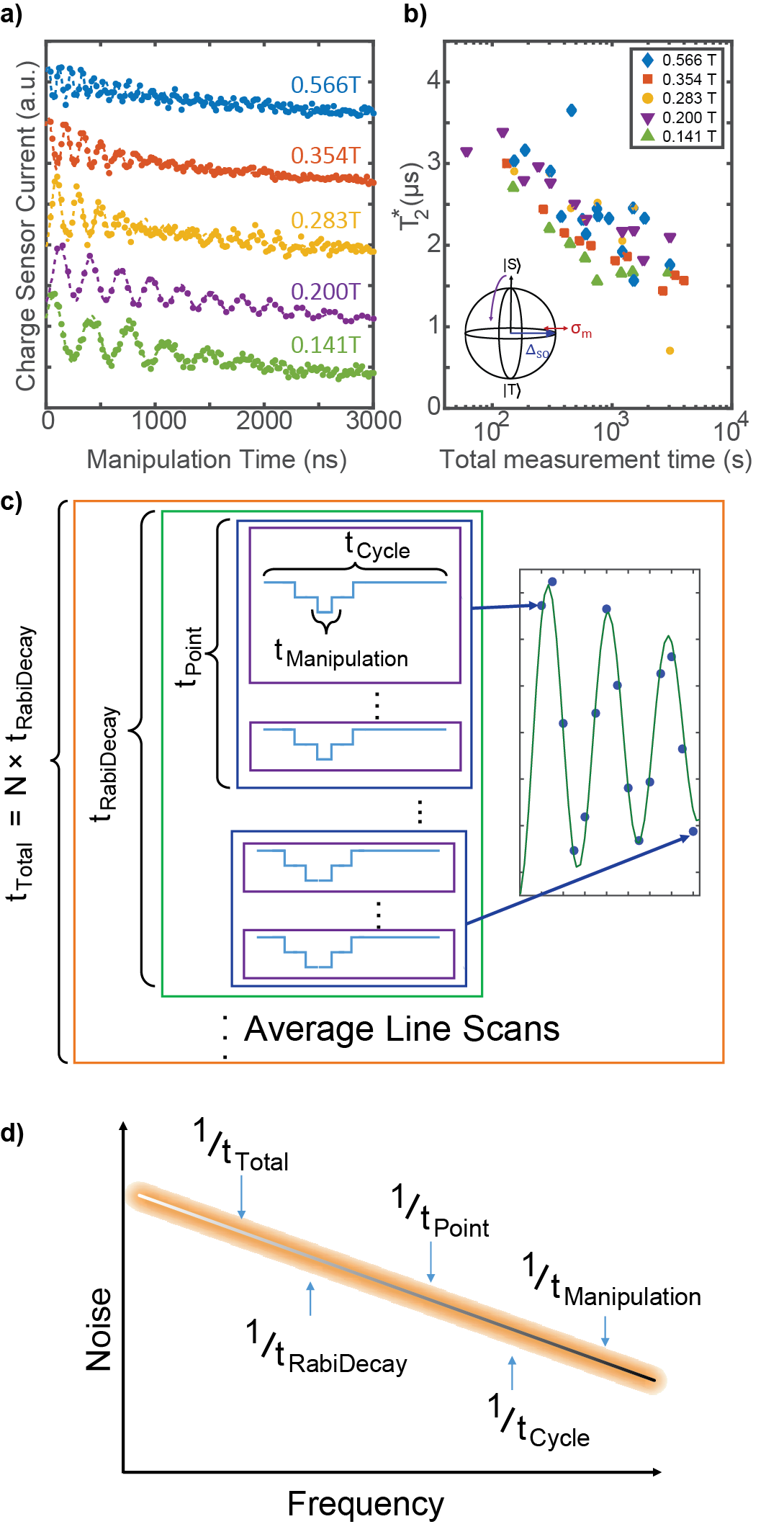
The ability to realize meaningful quantum information processing in MOS depends on the timescale over which environmental noise near the interface interacts with the qubit, Fig. 3(c,d). Although sparse, the background nuclear spins are sufficient in number to produce a slowly varying effective magnetic field, an Overhauser field. Nuclear spin flip-flops lead to a time-variation of the Overhauser field that is quasi-static on the timescale of a single measurement instance, but can shift the rotation frequency in the time interval between measurements. A consequence of this effect is that the decay in time of the coherent oscillations depends on the measurement integration time, as has been observed previously in ST qubits Dial et al. (2013); Eng et al. (2015). The longer an average measurement is done, the broader the distribution of spin configurations (i.e. Overhauser fields) sampled. The ensemble-averaged singlet return signal as a function of time spent driving rotations in the region, with an external magnetic field oriented along the crystallographic axis, is shown in Fig. 3(a). The decay in oscillation amplitude fits a Gaussian form consistent with quasi-static noise Dial et al. (2013), and characteristic is extracted assuming a functional time dependence of for the oscillation decay envelope.
In Fig 3(b) we examine the dependence of our results on measurement time and B-field. We find a long-averaging inhomogeneous dephasing time of , which is consistent with other experimental resultsWu et al. (2014); Eng et al. (2015) and theoretical estimatesAssali et al. (2011); Witzel et al. (2012a, b) (see supplementary material) of dephasing due to hyperfine coupling of the QD electron wave function with residual in the isotopically-enriched Si host. By measuring at faster timescales, an increased is observed. The absence of a B-field dependence suggests that the SO coupling does not contribute appreciably to . Therefore, the observed at the MOS interface is consistent with expectations of the enriched bulk Si and there is no evidence of slow noise due to the MOS interface at this enrichment level.
A second axis of coherent control for ST qubits is achieved through the tunable exchange coupling of the and charge states. This leads to hybridization between the and charge states and an exchange splitting, , between the and qubit states that depends on detuning, , Fig. 4(a). By varying the strength of this interaction, we can achieve controlled coherent rotations, as demonstrated in Fig. 4(b). Here, as described in Ref. Petta et al. (2005), we initialize into a ground state and then adiabatically separate the electrons into the charge configuration where is nearly zero and the qubit is initialized in the ground state of the SO field ( or ), a superposition of the and states. We apply a fast pulse to and from finite at near 0 for some waiting time, which rotates the qubit state around the Bloch sphere about a rotation axis depending on both and , the SO induced splitting of the and states (Fig. 4(a)). For this experiment, we apply a field of 0.2 T along the direction, which provides a small (0.5 MHz) residual -rotation frequency. At detuning near = 0, we observe an increased rotation frequency, Fig 4(c). As the exchange pulse moves to deeper detuning, we observe a decrease in rotation frequency as well as visibility. This is expected as decreases and the rotation axis tilts towards the direction of the SO field difference.
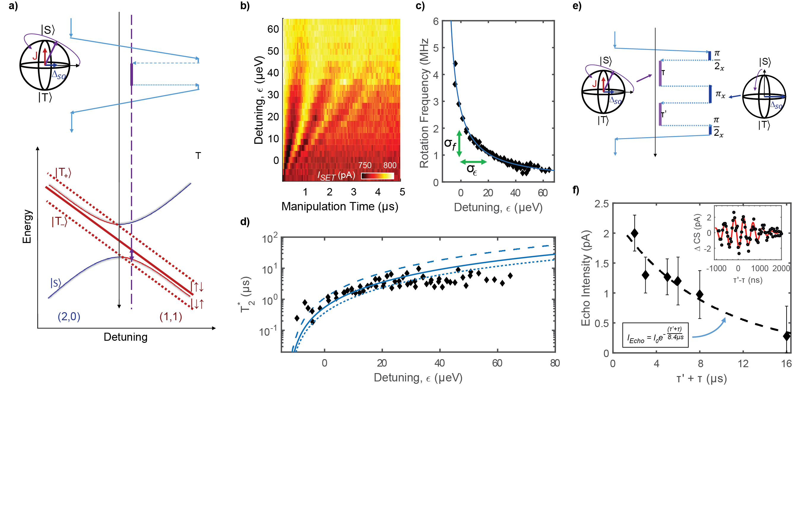
Figure 4(c) shows the observed rotation frequency as a function of detuning. The rotation frequency can be expressed as , since the two components add in quadrature. Indeed, we see that at deep detuning the rotation frequency saturates near 0.5 MHz, due to the SO field at this magnetic field strength and orientation. Figure 4(d) shows the dephasing time, , associated with coherent rotations at each detuning. Here we have extracted by fitting a Gaussian decay envelope () to the rotations at each detuning point. Noise from charge fluctuations on the confinement gates causes deviations in the detuning point of the system, leading to dephasing of the qubit through changes in the rotation frequency. We measure shorter dephasing time near , which increases as we move to deeper detuning and eventually saturates at a few s. We associate the saturation of at deeper detuning with the dominant noise mechanism transitioning from charge to magnetic noise due to residual background . Following the method outlined in Ref. Dial et al. (2013), we fit the rotation frequency to a smooth function to find the derivative, . The ratio of to gives a root-mean-squared charge noise of . This agreement with the best reported charge noise values in GaAs/AlGaAs and Si/SiGe material systems of a few eV Petersson et al. (2010); Shi et al. (2013); Dial et al. (2013); Wu et al. (2014) indicates that the poly-silicon MOS device structure is a comparable material system with respect to the magnitude of quasi-static charge noise in the limit of long time integration. Furthermore, successive measurements over the course of several weeks can be performed with no retuning of the device gate voltages, indicating that the MOS material system is an extremely stable qubit platform.
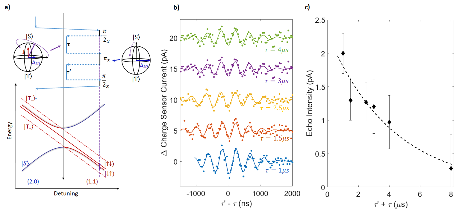
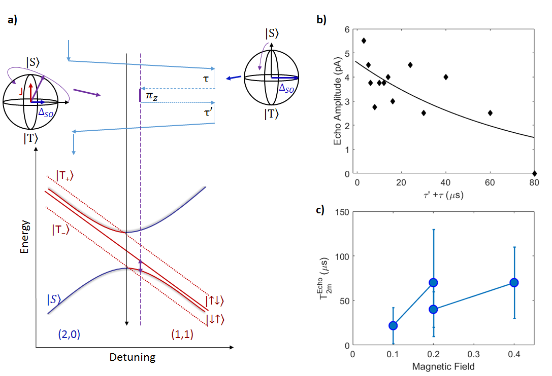
Improved decoherence can be achieved through dynamical decoupling (DD), which suppresses contributions from quasi-static noise through multi-rotation sequences that leverage time reversal symmetry. A schematic for a Hahn-echo sequence to examine electrical noise is shown in Fig. 4(e). As seen in Fig. 4(f), a refocusing pulse can greatly extend the qubit coherence with a of 8.4 s for a detuning, , where charge noise leads to = 1 s. This is comparable to what has been observed in GaAs/AlGaAsDial et al. (2013) and Si/SiGeEng et al. (2015). Likewise, Hahn-echo techniques were able to improve decoherence from magnetic noise to a of 70 s (see supplementary material). These results illustrate our ability to extend coherence times through dynamical decoupling and unequivocally demonstrate full all-electrical control of the MOS spin-orbit driven ST qubit.
III Summary
In previous implementations of ST qubits, dynamic nuclear polarization (DNP)Foletti et al. (2009); Nichol et al. (2017) and micro-magnetsWu et al. (2014) have been used to create strong, stable difference in Zeeman splitting between two quantum dots and drive rotations. DNP produces a variation in the nuclear magnetic field between dots. However, this gradient must be actively pumped and the qubit is susceptible to fluctuations in the nuclear magnetic environment. A second approach, micro-magnet integration, has been used to produce static magnetic fields and allows operation in an enriched host environment. However, this additional fabrication complexity creates long-term integration challenges for extending to larger qubit systems (e.g. non-standard fabrication, uniformity, and layout constraints). Additionally, single nuclear spin-driven ST rotation has been demonstrated recently using phosphorus in enriched Si, which overcomes these challengesHarvey-Collard et al. (2015); Rudolph et al. (2017). However, deterministic fabrication with donors is non-trivial and remains a topic of ongoing research. In contrast to these other options, the SO driven ST qubit offers a relatively simple MOS implementation path.
The SO -rotations have reached 20 MHz in our device, limited primarily by preparation and readout constraints. Though this is larger than what has been reported for a ST qubit in Si/SiGe using a micro-magnetWu et al. (2014), it is smaller than a number of other implementations mentioned above that have achieved 50 to 1000 MHz Harvey-Collard et al. (2015); Nichol et al. (2017); Takeda et al. (2016). Increased drive frequency with SO coupling is likely possible through a number of avenues, including increasing vertical E-field (see supplementary material and Ref. Veldhorst et al. (2015b)), modifying the confinement potential (see SM), and by working with one of the QDs at higher occupation (since the two z-valleys at the hetero-interface are predicted to have opposite sign of the Dresselhaus strength (see SM and Refs. Veldhorst et al. (2015b); Ferdous et al. (2017a, b))). Single QDs have displayed a 140 MHz difference in ESR frequencies between N = 1 and N = 3 and E-field tunabilityVeldhorst et al. (2015b), so drive frequencies of over 100 MHz seem realistic. This work also provides a theoretical foundation for an interface Dresselhaus and Rashba effect that avoids quantitative ambiguities due to gauge-dependence. This is relevant for devices that rely on SO effects at semiconductor interfaces, including emerging areas of research in topological quantum materials. Furthermore, future work also remains to establish how the microscopic details of the MOS interface affect the magnitudes of the Rashba and Dresselhaus terms. Considering the possibilities for improvement and the reduced complexity in fabrication, the SO driven ST qubit offers a promising new implementation for quantum information technology.
Most significantly from this work, the SO driven ST qubit allows for a sensitive probe of noise properties at the MOS interface. The of order 1-2 s observed in the magnetic noise dominated regime is consistent with decoherence expected from in the bulk. Charge noise magnitudes of at are also comparable to other semiconductor systems. Overall, the MOS interface shows no indication of increased negative effects relative to qubit operation. The opportunity to use MOS for highly sensitive spin coherent devices such as qubits has broad impact.
IV Methods
The DQD studied in this work was realized in a fully foundry-compatible, single-gate-layer, isotopically-enriched metal-oxide-semiconductor (MOS) device structure. The material stack consists of 200 nm of n poly-silicon and 35 nm of silicon-oxide on top of a silicon substrate with an isotopically enriched epitaxial layer hosting 500ppm residual . The confinement and depletion gates are defined by electron beam lithography followed by selective dry etching of the poly-silicon. Phosphorus donors were implanted through a self-aligned implant window near the QD locations for alternative experiments. This was followed by an activation annealing process at 900 C. Biasing the poly-silicon gates confines a 2-dimensional electron gas into quantum dot potentials. One QD is used as a single electron transistor (SET) remote charge sensor for spin-to-charge conversion. The rest of the device is tuned such that a double quantum dot (DQD) is formed and the number of electrons in each QD is inferred from changes in current through the SET. Measurements were performed in a / dilution refrigerator with a base temperature of around 8 mK. The effective electron temperature in the device was 150 mK. Fast RF lines we connected to cryogenic RC bias-T’s on the sample board, which to allow for the application of fast gate pulses. An external magnetic field was applied using a 3-axis vector magnet. Additional information discussing the device and measurements is offered in the supplementary material and elsewhereRochette et al. (2017).
V Acknowledgements
We would like to thank Rusko Ruskov for discussions. This work was performed, in part, at the Center for Integrated Nanotechnologies, an Office of Science User Facility operated for the U.S. Department of Energy (DOE) Office of Science by Los Alamos National Laboratory (Contract DE-AC52-06NA25396) and Sandia National Laboratories (Contract DE-NA-0003525). Sandia National Laboratories is a multimission laboratory managed and operated by National Technology and Engineering Solutions of Sandia, LLC, a wholly owned subsidiary of Honeywell International, Inc., for the DOE’s National Nuclear Security Administration under contract DE-NA0003525.
VI Author Contributions
R.M.J, P.H.-C., and M.S.C. designed the experiments. R.M.J. performed the central measurements and analysis presented in this work. P.H.-C. performed supporting measurements on a similar device that establish repeatability of observations. N.T.J. developed the theoretical description of the results with the help of A.M.M., V.S., J.K.G., A.D.B., and W.M.W., providing critical insights. R.M.J., M.S.C., N.T.J., P.H.-C., A.M.M. and M.R. analyzed and discussed central results throughout the project. D.R.W., J.A., R.P.M., J.R.W., T.P., and M.S.C. designed the process flow, fabricated devices, and designed/characterized the 28Si material growth for this work. J.R.W. provided critical nanolithography steps. M.S.C. supervised the combined effort, including coordinating fabrication and identifying modeling needs for the experimental path. R.M.J. and M.S.C. wrote the manuscript with input from all co-authors.
References
- Vandersypen et al. (2016) L. M. K. Vandersypen, H. Bluhm, J. S. Clarke, A. S. Dzurak, R. Ishihara, A. Morello, D. J. Reilly, L. R. Schreiber, and M. Veldhorst, arXiv.org (2016), arXiv:1612.05936 .
- Petersson et al. (2010) K. Petersson, P. J.R., L. H, and G. A.C., Physical Review Letters 105, 246804 (2010).
- Shi et al. (2013) Z. Shi, C. B. Simmons, D. R. Ward, J. R. Prance, R. T. Mohr, T. S. Koh, J. K. Gamble, X. Wu, D. E. Savage, M. G. Lagally, M. Friesen, S. N. Coppersmith, and M. A. Eriksson, Phys. Rev. B 88, 075416 (2013).
- Dial et al. (2013) O. E. Dial, M. D. Shulman, S. P. Harvey, H. Bluhm, V. Umansky, and A. Yacoby, Physical Review Letters 110, 146804 (2013).
- Wu et al. (2014) X. Wu, D. R. Ward, J. R. Prance, D. Kim, J. K. Gamble, R. T. Mohr, Z. Shi, D. E. Savage, M. G. Lagally, M. Friesen, S. N. Coppersmith, and M. A. Eriksson, Proceedings of the National Academy of Sciences 111, 11938 (2014), http://www.pnas.org/content/111/33/11938.full.pdf .
- Harvey-Collard et al. (2015) P. Harvey-Collard, N. T. Jacobson, M. lph, J. Dominguez, G. A. Ten Eyck, J. R. Wendt, T. Pluym, J. K. Gamble, M. P. Lilly, M. Pioro-Ladrière, and M. S. Carroll, arXiv.org (2015), 1512.01606v1 .
- Eng et al. (2015) K. Eng, T. D. Ladd, A. Smith, M. G. Borselli, A. A. Kiselev, B. H. Fong, K. S. Holabird, T. M. Hazard, B. Huang, P. W. Deelman, I. Milosavljevic, A. E. Schmitz, R. S. Ross, M. F. Gyure, and A. T. Hunter, Science Advances 1, e1500214 (2015).
- Rudolph et al. (2017) M. Rudolph, P. Harvey-Collard, R. Jock, T. Jacobson, J. Wendt, T. Pluym, J. Domínguez, G. Ten-Eyck, R. Manginell, M. P. Lilly, and M. S. Carroll, arXiv.org (2017), arXiv:1705.05887 .
- Gamble et al. (2016) J. K. Gamble, P. Harvey-Collard, N. T. Jacobson, A. D. Baczewski, E. Nielsen, L. Maurer, I. Montaño, M. Rudolph, M. S. Carroll, C. H. Yang, A. Rossi, A. S. Dzurak, and R. P. Muller, Applied Physics Letters 109, 253101 (2016), http://aip.scitation.org/doi/pdf/10.1063/1.4972514 .
- Veldhorst et al. (2014) M. Veldhorst, J. C. C. Hwang, C. H. Yang, A. W. Leenstra, B. de Ronde, J. P. Dehollain, J. T. Muhonen, F. Hudson, K. M. Itoh, A. Morello, and A. S. Dzurak, Nature Nanotechnology 9, 981 (2014).
- Veldhorst et al. (2015a) M. Veldhorst, C. H. Yang, J. C. C. Hwang, W. Huang, J. P. Dehollain, J. T. Muhonen, S. Simmons, A. Laucht, F. E. Hudson, K. M. Itoh, A. Morello, and A. S. Dzurak, Nature 526, 410 (2015a).
- Ralls et al. (1984) K. S. Ralls, W. J. Skocpol, L. D. Jackel, R. E. Howard, L. A. Fetter, R. W. Epworth, and D. M. Tennant, Phys. Rev. Lett. 52, 228 (1984).
- Culcer and Zimmerman (2013) D. Culcer and N. M. Zimmerman, Applied Physics Letters 102, 232108 (2013), http://dx.doi.org/10.1063/1.4810911 .
- Borselli et al. (2011) M. G. Borselli, K. Eng, E. T. Croke, B. M. Maune, B. Huang, R. S. Ross, A. A. Kiselev, P. W. Deelman, I. Alvarado-Rodriguez, A. E. Schmitz, M. Sokolich, K. S. Holabird, T. M. Hazard, M. F. Gyure, and A. T. Hunter, Applied Physics Letters 99, 063109 (2011), http://dx.doi.org/10.1063/1.3623479 .
- Jones et al. (2016) C. Jones, M. A. Fogarty, A. Morello, M. F. Gyure, A. S. Dzurak, and T. D. Ladd, (2016), arXiv:1608.06335 .
- Veldhorst et al. (2015b) M. Veldhorst, R. Ruskov, C. H. Yang, J. C. C. Hwang, F. E. Hudson, M. E. Flatté, C. Tahan, K. M. Itoh, A. Morello, and A. S. Dzurak, Phys. Rev. B 92, 201401 (2015b).
- Ferdous et al. (2017a) R. Ferdous, E. Kawakami, P. Scarlino, M. P. Nowak, D. R. Ward, D. E. Savage, M. G. Lagally, S. N. Coppersmith, M. Friesen, M. A. Eriksson, L. M. K. Vandersypen, and R. Rahman, arXiv.org (2017a), arXiv:1702.06210 .
- Ferdous et al. (2017b) R. Ferdous, K. W. Chan, M. Veldhorst, J. Hwang, C. H. Yang, G. Klimeck, A. Morello, A. S. Dzurak, and R. Rahman, arXiv.org (2017b), arXiv:1703.03840 .
- Pfund et al. (2007) A. Pfund, I. Shorubalko, K. Ensslin, and R. Leturcq, Phys. Rev. Lett. 99, 036801 (2007).
- Fasth et al. (2007) C. Fasth, A. Fuhrer, L. Samuelson, V. N. Golovach, and D. Loss, Phys. Rev. Lett. 98, 266801 (2007).
- Nadj-Perge et al. (2010a) S. Nadj-Perge, S. M. Frolov, J. W. W. van Tilburg, J. Danon, Y. V. Nazarov, R. Algra, E. P. A. M. Bakkers, and L. P. Kouwenhoven, Phys. Rev. B 81, 201305 (2010a).
- Nadj-Perge et al. (2010b) S. Nadj-Perge, S. M. Frolov, E. P. A. M. Bakkers, and L. P. Kouwenhoven, Nature 468, 1084 (2010b).
- Stepanenko et al. (2012) D. Stepanenko, M. Rudner, B. I. Halperin, and D. Loss, Phys. Rev. B 85, 075416 (2012).
- Rančić and Burkard (2014) M. J. Rančić and G. Burkard, Phys. Rev. B 90, 245305 (2014).
- Scarlino et al. (2014) P. Scarlino, E. Kawakami, P. Stano, M. Shafiei, C. Reichl, W. Wegscheider, and L. M. K. Vandersypen, Phys. Rev. Lett. 113, 256802 (2014).
- Nichol et al. (2015) J. M. Nichol, Harvey, S. P., M. D. Shulman, A. Pal, Umansky, R. Vladimir, E. I., Halperin, B. I., and A. Yacoby, Nature Communications 6, 7682 (2015).
- Rössler and Kainz (2002) U. Rössler and J. Kainz, Solid State Communications 121, 313 (2002).
- Golub and Ivchenko (2004) L. E. Golub and E. L. Ivchenko, Phys. Rev. B 69, 115333 (2004).
- Nestoklon et al. (2006) M. O. Nestoklon, L. E. Golub, and E. L. Ivchenko, Phys. Rev. B 73, 235334 (2006).
- Prada et al. (2011) M. Prada, G. Klimeck, and R. Joynt, New Journal of Physics 13, 013009 (2011).
- Nestoklon et al. (2008) M. O. Nestoklon, E. L. Ivchenko, J.-M. Jancu, and P. Voisin, Phys. Rev. B 77, 155328 (2008).
- Alekseev and Nestoklon (2017) P. S. Alekseev and M. O. Nestoklon, Phys. Rev. B 95, 125303 (2017).
- Manchon et al. (2015) A. Manchon, H. C. Koo, J. Nitta, S. M. Frolov, and R. A. Duine, Nature Materials 14, 871 (2015).
- Soumyanarayanan et al. (2015) A. Soumyanarayanan, N. Reyren, A. Fert, and C. Panagopoulos, Nature 539, 509 (2015).
- Lidar et al. (1998) D. A. Lidar, I. L. Chuang, and K. B. Whaley, Phys. Rev. Lett. 81, 2594 (1998).
- Harvey-Collard et al. (2017) P. Harvey-Collard, B. T. D’Anjou, M. Rudolph, N. Jacobson, J. Dominguez, G. A. Ten Eyck, J. R. Wendt, T. Pluym, W. A. Lilly, Michael Pand Coish, M. Pioro-Ladrière, and M. S. Carroll, arXiv.org (2017), 1703.02651 .
- Yang et al. (2013) C. H. Yang, A. Rossi, R. Ruskov, N. S. Lai, F. A. Mohiyaddin, S. Lee, C. Tahan, G. Klimeck, A. Morello, and A. S. Dzurak, Nat Commun 4, 2069 (2013).
- Tahan and Joynt (2014) C. Tahan and R. Joynt, Phys. Rev. B 89, 075302 (2014).
- Hwang et al. (2017) J. C. C. Hwang, C. H. Yang, M. Veldhorst, N. Hendrickx, M. A. Fogarty, W. Huang, F. E. Hudson, A. Morello, and A. S. Dzurak, arXiv.org (2017), arXiv:1608.07748 .
- Assali et al. (2011) L. V. C. Assali, H. M. Petrilli, R. B. Capaz, B. Koiller, X. Hu, and S. Das Sarma, Phys. Rev. B 83, 165301 (2011).
- Witzel et al. (2012a) W. M. Witzel, R. Rahman, and M. S. Carroll, Phys. Rev. B 85, 205312 (2012a).
- Witzel et al. (2012b) W. M. Witzel, M. S. Carroll, L. Cywiński, and S. Das Sarma, Phys. Rev. B 86, 035452 (2012b).
- Petta et al. (2005) J. R. Petta, A. C. Johnson, J. M. Taylor, E. A. Laird, A. Yacoby, M. D. Lukin, C. M. Marcus, M. P. Hanson, and A. C. Gossard, Science 309, 2180 (2005).
- Foletti et al. (2009) S. Foletti, H. Bluhm, D. Mahalu, V. Umansky, and A. Yacoby, Nature Physics 5, 903 (2009).
- Nichol et al. (2017) J. M. Nichol, L. A. Orona, S. P. Harvey, S. Fallahi, G. C. Gardner, M. J. Manfra, and A. Yacoby, npj Quantum Information 3 (2017).
- Takeda et al. (2016) K. Takeda, J. Kamioka, T. Otsuka, J. Yoneda, T. Nakajima, M. R. Delbecq, S. Amaha, G. Allison, T. Kodera, S. Oda, and S. Tarucha, Science Advances 2 (2016), 10.1126/sciadv.1600694.
- Rochette et al. (2017) S. Rochette, M. Rudolph, A.-M. Roy, M. Curry, G. Ten Eyck, R. Manginell, J. Wendt, T. Pluym, S. M. Carr, D. Ward, M. P. Lilly, M. S. Carroll, and M. Pioro-Ladrière, in progress (2017).
- Kawakami et al. (2014) E. Kawakami, P. Scarlino, D. R. Ward, F. R. Braakman, D. E. Savage, M. G. Lagally, M. Friesen, S. N. Coppersmith, M. A. Eriksson, and L. M. K. Vandersypen, Nature Nanotechnology 9, 666 (2014).
- Gamble et al. (2015) J. K. Gamble, N. T. Jacobson, E. Nielsen, A. D. Baczewski, J. E. Moussa, I. Montaño, and R. P. Muller, Physical Review B 91 (2015).
- Friesen et al. (2007) M. Friesen, S. Chutia, C. Tahan, and S. N. Coppersmith, Phys. Rev. B 75, 115318 (2007).
- Johnson et al. (2005) A. C. Johnson, J. R. Petta, C. M. Marcus, M. P. Hanson, and A. C. Gossard, Phys. Rev. B 72, 165308 (2005).
- Hahn (1950) E. L. Hahn, Phys. Rev. 80, 580 (1950).
VII Supplementary Information
.1 Spin-orbit Coupling at the MOS Interface
While spin-orbit (SO) coupling in bulk silicon is weaker than in other materials commonly used for quantum dot devices, such as GaAs and InAs, an interface introduces SO coupling that may significantly influence qubit operation. Such effects have been documented recently elsewhere in the case of a single quantum dot in silicon Kawakami et al. (2014); Veldhorst et al. (2014, 2015b); Ferdous et al. (2017a, b). Here, we detail our model for the SO coupling associated with the interface. Our theoretical treatment is informed by the previous work of Refs Nestoklon et al. (2006, 2008); Prada et al. (2011); Veldhorst et al. (2015b).
The Hamiltonian for a single electron in a silicon quantum dot in an arbitrary uniform magnetic field , without SO coupling included, is given by
where is the kinetic momentum (), () is the transverse (longitudinal) effective mass, and is the bulk -tensor for silicon. We take our coordinate system to be aligned along the Cartesian , , axes, with the interface normal. The potential includes electrostatic confinement from voltages applied to gate electrodes and details of the interface potential. Atomic-scale features at the interface, the potential barrier height, and the vertical electric field dictate the valley splitting and valley content of the valley-orbital eigenstates Gamble et al. (2016). Due to the strong vertical confinement, the low-lying valley-orbital eigenstates include contributions only from the conduction band minima. As a consequence of the weak bulk SO coupling in silicon, and are close to the vacuum -factor of 2.0. In our double quantum dot device the bulk -factor anisotropy, being common to both dots, does not manifest in significant measurable effects. The specific gauge choice for has no influence on any physical observables, and we emphasize that any theoretical analysis must be gauge-invariant. When necessary for numerical calculations, we choose the convenient gauge .
Assuming that we have found the valley-orbital eigenstates of the spin-independent part of , , we now treat the SO coupling as a perturbation. Following Refs Nestoklon et al. (2006, 2008); Prada et al. (2011); Veldhorst et al. (2015b), we take the SO interaction for an electron confined against an interface at to consist of both Rashba and Dresselhaus terms, and , respectively Golub and Ivchenko (2004). We emphasize the importance of the interface-localized -function in these terms. As we will see, this leads to the SO coupling appearing at first order in perturbation theory, rather than second order if the SO coupling had taken the bulk form without the interface-localizing -function. This latter property can be seen from the fact that, for bound valley-orbital eigenstates , the diagonal momentum matrix elements vanish, , without approximation. This can be confirmed by applying the commutation identities , , and . However, the interface-constrained diagonal matrix elements may be non-zero, in general, due to the cyclotron orbits established by an applied magnetic field. Note that, due to the crystal symmetry of silicon, a vertical shift of a pristine interface by , where is the lattice constant, is equivalent to an in-plane rotation by an angle . Consequently, while a Rashba term is invariant, a Dresselhaus term must change sign under such a transformationNestoklon et al. (2008), since a rotation maps , , , and . Hence, we assign the Dresselhaus coupling factor a dependence to capture the rapidly oscillatory behavior of the sign of the Dresselhaus coupling as a function of interface position.
To proceed with identifying the contributions of , we must evaluate the interface-constrained momentum matrix elements as a function of the applied magnetic field, . We note that the effective SO coupling strengths and should be expected to depend intimately on the atomistic details of the interface Nestoklon et al. (2006, 2008); Prada et al. (2011). For the purposes of this analysis, we wrap such details into Rashba and Dresselhaus coupling strengths and , respectively, and treat them as fit parameters. Future work will address the question of capturing the short length-scale physics of interface SO effects within a multi-valley effective mass theory frameworkGamble et al. (2015), in the spirit of previous analyses of valley splitting statistics in the presence of interface disorderGamble et al. (2016).
The valley composition of the valley-orbital eigenstates is dictated by the relative phase between the and valley components. Within a simplified envelope function picture (see e.g. Ref. Friesen et al. (2007)), the low-lying valley components are given by
| (4) | |||||
| (5) |
where is the position of the conduction band minimum, are the lattice-commensurate Bloch functions for silicon’s conduction band minima, and is an envelope function. The lowest two valley-orbital eigenstates are, then
| (6) | |||||
| (7) |
where is the valley phase factor. As mentioned previously, the value of and the valley splitting is dictated by details of the interface and associated confinement potential.
In particular, we approximate
| (8) |
where
| (9) |
with the envelope function and an unknown real parameter that depends on details of the Bloch function at the interface. Similarly, for the first excited valley state we’d obtain
| (10) |
To investigate the momentum matrix element with respect to the envelope function, we have implemented a (valley-free) finite-difference discretization of a Hamiltonian for a quantum dot that is harmonically confined laterally, with a uniform vertical electric field and an interface with energy offset ,
The harmonic confinement energies , are allowed to be distinct, describing an anisotropically-shaped quantum dot. From qualitative fits to a numerical analysis, we find the following functional form for the matrix elements with respect to the ground state envelope function:
| (12) | |||||
| (13) |
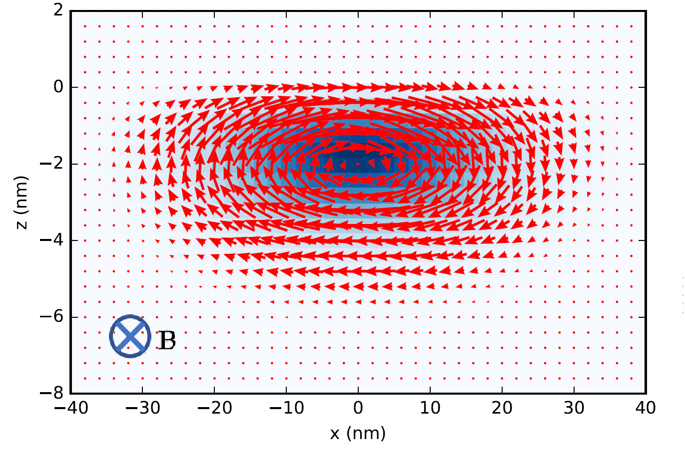
where for dot confinement energies of we find . The dependence is consistent with what is expected for a triangular vertical confinement potential Veldhorst et al. (2015b). Notice that these matrix elements depend weakly on the lateral confinement energies, with the dominant dependence on the vertical electric field and transverse magnetic field. This qualitative functional dependence on magnetic and vertical electric fields is consistent with the analysis of Ref Veldhorst et al. (2015b). In Fig. 5, we plot a representative momentum density, indicating the cyclotron orbits induced by the applied magnetic field.
Combining the envelope function and valley components together, we obtain the following functional form for the interface-constrained momentum matrix elements:
| (14) | |||||
| (15) | |||||
where is a function that encodes the dependence on valley phase, interface location, vertical electric field, and lateral confinement.
While the SO interaction will induce non-zero matrix elements between valley-orbital eigenstates such as , the influence of these matrix elements will be suppressed by the valley splitting Veldhorst et al. (2015b). Since valley splitting in MOS systems is typically relatively large ( in this experiment) and these inter-valley eigenstate matrix elements appear to second order in perturbation theory, we neglect them here.
Within the subspace spanned by the tensor product of the lowest valley-orbital eigenstate and spin eigenstates , , , we can express the SO Hamiltonian as
| (16) |
If we make the approximation that the dot is nearly symmetric, , then this reduces to the form
| (17) | |||||
where
| (18) |
Consequently, the interface SO interaction in a quantum dot can be represented as a modified -tensor = , where
| (19) |
Note here that the total -tensor need not be symmetric, since any asymmetry in the quantum dot geometry may result in , in general. However, in our fitting to the present experimental data we have observed satisfactory agreement when assuming a symmetric -tensor. Future measurements with reduced statistical uncertainty or more anisotropic dot geometries may allow for this effect to be probed.
In the regime of deep detuning, for which the two electrons in the DQD are well delocalized into the charge configuration, we can treat the interface SO coupling as producing a distinct effective -tensor in the left and right dots, and . That is, the SO Hamiltonian transforms the Zeeman Hamiltonian for the two-electron problem into
| (20) |
where () is the vector of Pauli operators acting on an electron in the left (right) quantum dot.
We now show how this -tensor difference appears in terms of the basis states , where we follow the convention of Ref. Stepanenko et al. (2012):
| (21) | |||||
where () creates an electron in the left (right) quantum dot with spin up in the eigenbasis of (relative to the crystallographic axis ) and is the zero-electron state. Given this set of basis states and defining
| (22) | |||||
we can now write down the Zeeman Hamiltonian incorporating SO coupling:
where
| (23) | |||||
| (24) | |||||
| (25) |
We now evaluate the unpolarized triplet spin eigenstate relative to the quantization axis dictated by the applied magnetic field, . Using the fact that the -tensor is only weakly perturbed from its bulk value, , and diagonalizing the 3x3 triplet block, we obtain
| (26) |
where the applied B-field is taken to be
| (27) |
with respect to the crystallographic axes , , and .
Finally, to evaluate the frequency of rotations generated by such a difference in -tensors, we need to evaluate the matrix element , where and are the singlet and unpolarized triplet states defined with respect to the spin basis of the applied uniform B-field defined above. We find that this rotation frequency is
| (28) | |||||
| (29) | |||||
| (30) |
From the above expression, it’s clear that applying a B-field normal to the interface will generate no effective magnetic field gradient. For an in-plane field, depending on the relative sign of the Rashba and Dresselhaus differences and , there will be an azimuthal angle that maximizes the generated rotation frequency. If (), the maximum rotation frequency will be obtained for (), i.e. B-field oriented along (). Conversely, for the minimum rotation frequency would be obtained for or , i.e. nearly aligned along the or Cartesian axes. In our experiment, with , the minimum frequency should be attained with a B-field about 3.5 degrees away from the orientation.
.2 Device Fabrication, Structure, Operation
.2.1 Device Structure
The singlet-triplet (ST) qubit studied in this work was fabricated in a fully foundry-compatible process using a single-gate-layer, metal-oxide-semiconductor (MOS) poly-silicon gate stack with an epitaxially-enriched 28Si epi-layer with 500ppm residual 29Si. Hall bars from the same sample wafer with the same gate oxide were used to extract the critical density ( = 5.7x10¹¹/cm2), the peak mobility ( =4500 cm2/Vs), threshold voltage ( = 1.1 V), the RMS interface roughness ( = 2.4 ), and roughness correlation length ( = 26 ). An SEM image of a device fabricated nominally identically to the one used in this work and a schematic of the gate stack are shown in Fig. S6(a,b). The device is operated in an enhancement mode using voltage biasing of the highly doped n+ poly-silicon gates to confine electrons to quantum dot (QD) potentials under gates LCP and UCP. The gates ULG, URG, LLG and LRG overlap with n+ regions and ohmic contacts and are biased to accumulate a two-dimensional electron gas (2DEG) under each gate. The 2DEGs act as source and drain electron reservoirs for the quantum dots. The lower half of the device is tuned such that a double quantum dot (DQD) is formed. One QD is tunnel coupled to the reservoir under LRG and the other quantum dot can only be occupied by electron tunneling through the first QD. The upper half of the device is used as a single electron transistor (SET) remote charge sensor. The SET is biased with 70 (rms) AC bias at 0V DC and the current is measured with an AC lock-in technique at 979 Hz. The electron temperature, 150 mK, was measured by QD charge transition line width. More details about fabrication can be located in Ref Rochette et al. (2017).
.2.2 Dot Occupation and Location
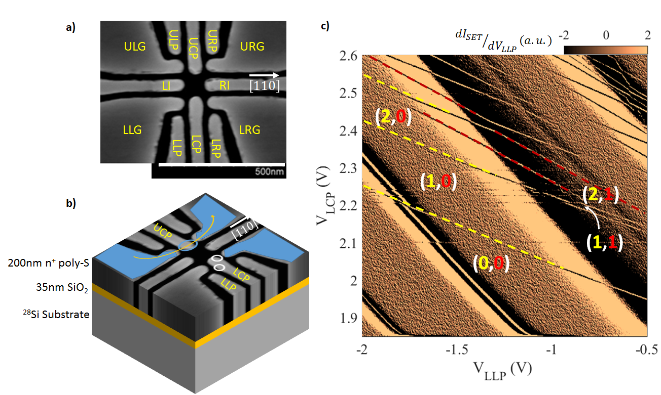
The number of electrons in each QD may be inferred from changes in current through the SET as depicted in Fig. S6(c). The collection of yellow parallel lines is assigned to a QD connected to the electron reservoir under LRG, which we call QD1. Counting from the left, we can identify the QD1 N=1 N=2 charging transition. A second object is observed anti-crossing with QD1, which we label as the N=0 N=1 charge transition for a second QD, QD2. A second line is observed belonging to QD2 in the scan, though disorder in the system makes identifying higher occupation lines difficult. However, the presence of Pauli spin blockade at the QD1-QD2, (2,0)-(1,1) anti-crossing identifies the system as a useful DQD for a ST qubit architecture (see Fig. S7). To determine the locations of QD1 and QD2 we can use their capacitances to the nearby poly-silicon gates. By scanning combinations of the poly-silicon gates (as seen in Fig. S6(c) for LLP and LCP), we can obtain the relative capacitance of both QDs to each gate compared to the capacitance of LCP, which has the strongest capacitive coupling to both QDs. We have tabulated the relative capacitances in Table 1.
| ci/cLCP | LLP | LRP | LI | RI | LLG | LRG |
|---|---|---|---|---|---|---|
| QD1 | 0.18 | 0.33 | 0.24 | 0.16 | 0.29 | 0.35 |
| QD2 | 0.27 | 0.22 | 0.13 | 0.14 | 0.29 | 0.10 |
These values allow for triangulation of the dot locations, which we have indicated in S6(b) with open circles. We differentiate QD2 from an implanted donor through several observations: (1) no hyperfine component in the rotation frequency, (2) the lack of rotations at 0T B-field, (3) the ramp rates required for adiabatic transfer through the spin gap are slower than what is expected for a donor, and (4) the presence of additional lines corresponding to the QD. We find that this layout systematically produces objects near the central QD with these capacitances when the gates opposite the electron reservoir 2DEG are at low biases. For experiments investigating single QDs, these voltage potential minima may be emptied with more negative voltages on LLP or flooded by accumulating a larger 2DEG under LLG with more positive voltages.
.2.3 Qubit Initialization, Operation and Readout
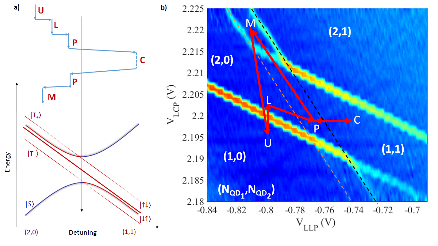
We operate this system near the (2,0) (1,1) spin-blockaded charge anti-crossing. An energy diagram for the two-electron system is shown in Fig. S7(b). The ground state charge configuration is determined by the detuning between dots, , which is controlled by tuning the voltages on gates LLP and LCP. These gates are connected to cryogenic RC bias-T’s which allow the application of fast gate pulses. A schematic of the cyclical pulse sequence is shown in Fig. S7(a), which is repeated as the current through the SET is monitored by the averaged AC lock-in measurements. The system is initialized in the (2,0) charge sector by first unloading (point U) the DQD into the (1,0) charge configuration and then applying an energy-selective pulse into the (2,0) charge state between the singlet and triplet energy levels such that a (2,0)S ground state is loaded (point L). The system is then plunged (point P) to a detuning ( 0) close to the charge anti-crossing. The electrons are then separated (point C) and qubit manipulations are performed in the (1,1) charge region ( 0). The system is then pulsed back to the (2,0) charge sector (point P) where, due to Pauli spin blockade, a singlet spin state is allowed to transfer to the (2,0) charge state, but a triplet spin state is energetically blocked and remains as a (1,1) charge state Johnson et al. (2005). We then use an enhanced latching mechanism for a spin-to-charge conversion (point M). This technique is presented in great detail in Harvey-Collard et al. (2017). There are several advantages for the use of this method. First, since an electron on the QD2 needs to tunnel through the QD1 to access an electron reservoir, the metastable latching state can be long lived. This allows for the measurement step in our cyclical pulse sequence to be long, compared to other points in the sequence, and dominate the time average. Second, in this approach, the charge-sensed signal differentiates between a (2,1) and a (2,0) charge state. In other words, the difference in measured current between a singlet and triplet state is the capacitive effect of adding an electron to QD2. Thus, it does not rely on the dipole orientation of the DQD, as in traditional Pauli-blockade measurement techniques. In our case, the DQD is oriented in such a way that differentiating a (2,0) and (1,1) charge state is exceptionally difficult (observe the lack of visible inter-dot transition line in Fig. S7(b)) and this method is necessary.
.3 Analysis Note on Extracted Data
.3.1 Qubit Rotation Frequency
Figure S8(a) shows the singlet return signal as a function of time spent at the manipulation point in as the strength of the external magnetic field is varied along the crystallographic direction up to 1.2 T. We see that, at high magnetic field, the oscillations are difficult to observe, since the Coulomb blockade peak used for charge sensing drifts as a function of magnetic field. The qubit rotation frequency at each field was found by fitting each line scan to a Gaussian decay of the form
| (31) |
where all parameters are free. To help with the visualization, we subtract the background linear portion to our charge sensor signal (, above), as shown in Fig. S8(b).The background slope in charge sensor current is due to imperfectly separating the two electrons, such that, for some fraction of the experiments, an electron diabatically transitions through the ani-crossing, thus inelastically transferring between S(2,0) and S(1,1) on the time scale of a few s. The rotation frequency, , corresponding to the data in Fig. S8(a) is plotted as a function of magnetic field in Fig. S8c, indicating a 20 MHz rotation frequency at the maximum field. As can be seen in Fig. S7(c), there are outlier points, which occur when a fit to equation (31), produces an unphysical periodic component.
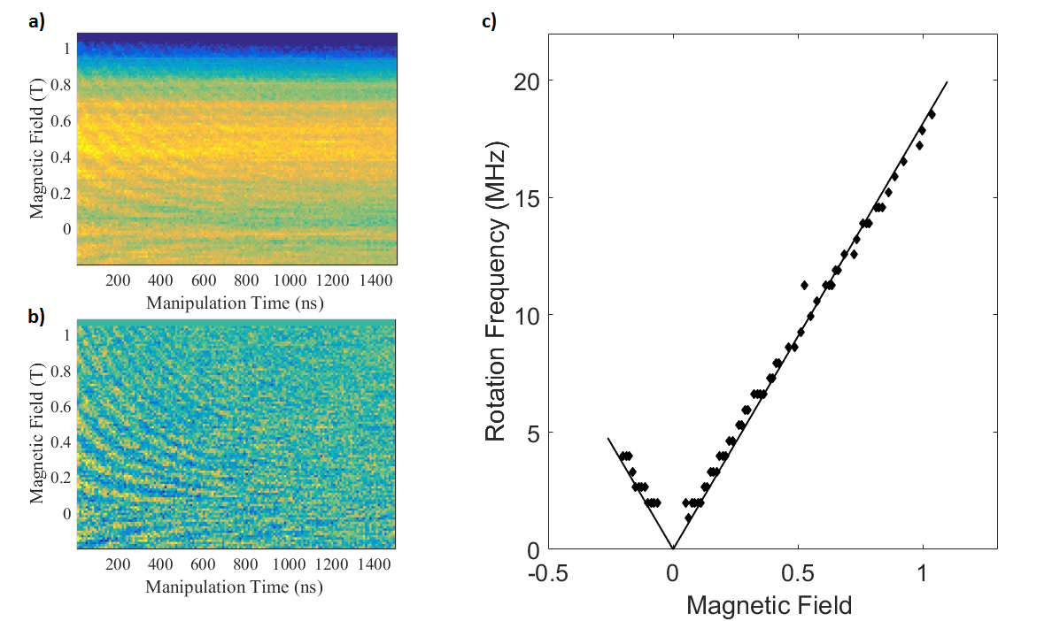
Similar techniques were used to analyze the data in the main text. The data presented in Figs. 2(c,e) of the main text were also obtained from magnetic field scan experiments and similar behavior was observed. A majority of the data fits well, and clear magnetic field strength and angular dependencies may be extracted. The data presented in Fig. 2(d), was taken with repeated scans at a given field strength and orientation. For Fig. 2(b), the linear portion of the background charge current sensor was subtracted, to clearly show the oscillations. This was useful, as slow timescale changes in the current through the charge sensor obscured the visualization.
.3.2 Charge Noise Characterization
Here we describe the procedure to extract charge noise, following Ref Dial et al. (2013). Several results in ST qubits have shown that a dominant source of dephasing during exchange oscillations can be modeled as gate-referred, quasi-static voltage fluctuations on nearby gatesDial et al. (2013); Eng et al. (2015). These voltage fluctuations affect the energy detuning between dots, materializing as fluctuations in the exchange energy, . At a given detuning, the qubit will rotate at a frequency about the Bloch sphere
| (32) |
Therefore, we expect noise in detuning to create noise in the rotation frequency . For charge noise that is quasi-static, we expect a Gaussian decay of the oscillations of the form , where is the inhomogeneous dephasing time which is related to the root-mean-squared charge noise by
| (33) |
is found for each detuning point by fitting the oscillations to Gaussian decay as shown in Fig. 4(a) of the main text. A functional form of ) is found by fitting the data in Fig. 4(c) to a smooth function. We approximate the exchange energy as ,where , where is the full-gap, inter-dot tunnel coupling, and find a good fit to . We extract 0.7 eV from the fit. From the ratio of to , for detunings less than 30 eV, a charge noise figure of = 2.0 0.6 eV can be extracted. This value agrees with reported charge noise numbers of a few eVPetersson et al. (2010); Shi et al. (2013); Dial et al. (2013); Wu et al. (2014), indicating that proximity to the MOS interface does not degrade the qubit.
.3.3 Magnitude
Several theoretical estimates of in isotopically enriched silicon have been presented in the literatureAssali et al. (2011); Witzel et al. (2012a, b). The estimate by Assali et. al. gives a of 4.4 s for the corresponding isotopic enrichment used in our experiments (500 ppm). Note: We have included a factor of 2 because the calculations in in Ref. Assali et al. (2011) do not account for of the 29Si nuclei. Witzel et. al., on the other hand, predict a of a few tens of s, though they use a substantially larger QD radius. Following the central limit theorem, we expect , where is the number of spinful nuclei within the QD wavefunction, and that a decrease in QD size will lead to a decrease in the inhomogeneous dephasing time.
Furthermore, these reports consider single quantum dots. We are concerned with a DQD, in which each QD has a separate distribution of nuclear spins and the changes in the difference in hyperfine fields between QDs leads to the ST dephasing. Therefore, is inversely proportional to the amount of fluctuations in the surrounding hyperfine field. If we say that each quantum dot has a normal distribution of hyperfine fields of the form
| (34) |
where is the variance in hyperfine field and is the average hyperfine field, then the distribution of the difference in hyperfine field between the two dots is given by,
| (35) |
This is a normal distribution with a variance of and an average difference in Hyperfine field of . Thus, we expect
| (36) |
assuming similar sized QDs. Taking into account the differences in QD size and the effect of two QDs, which both imply a reduction in , our measured value of 1.6 s fits well with these order of magnitude estimates.
.3.4 Measurement Time Dependence of

Figure 3(b) of the main text displays a clear dependence of on the total experimental measurement time. This effect has been reported previouslyDial et al. (2013); Eng et al. (2015), and is due to the time dynamics of the random hyperfine field from the residual 500 ppm 29Si in the isotopically purified silicon host. Fluctuations in the polarization of the nuclei lead to varying magnetic fields at each QD between each experiment cycle. This leads to a varying qubit rotation frequency in each experimental cycle, which, as they are averaged together, lead to a decay in oscillation amplitude. As the experiment is measured for longer times, a larger sample of random nuclei polarization configurations, and a correspondingly larger distribution of qubit rotation frequencies is sampled.
To obtain the plot in Figure 3(b), we repeat a measurement of charge sensor current versus manipulation time many times. An example of such a plot is shown in Fig. S9(a) for a magnetic field of 0.2 T along the [110] direction. By averaging various numbers of line scans together, we can examine the effect of measurement time on . Here, the total measurement time is the time for one experimental line scan times the number of scans averaged, and is extracted by fitting the envelope of the averaged data to a Gaussian decay (). Examples of the averaged data for averaging 5 and 50 line scans are shown in Fig. S9(b).
.3.5 Hahn-Echo Measurements
The experiments presented in this work indicate that the dephasing of the qubit during rotations is predominantly due to low-frequency, quasi-static noise. Dynamical decoupling techniques may be used to prolong qubit coherence. This method effectively filters the noise, such that qubit dephasing is most sensitive to noise around the experimental manipulation time. In this work we use a Hahn echo technique Hahn (1950) to decouple from low frequency charge and magnetic noise. To perform a charge noise Hahn echo, a pulse sequence as detailed in Ref. Dial et al. (2013) and depicted in Fig. S10(a) is used. For the results presented in the main text, we operated the qubit at a B-field of 0.141 T along the [110] direction giving an X-rotation frequency of = 2.03 MHz. We investigate the effect of a Hahn echo pulse sequence on charge noise decoherence at a detuning where the qubit rotation frequency is 2.24 MHz, corresponding to = 0.99 MHz (). In Fig. S10(b) the measured echo signal is plotted as a function of the difference in evolution times for the first and second -pulse ( - ) for several total evolution times (). Here we have subtracted the background charge sensor current, leaving the echoed signal. The echo displays oscillations at 2.24 MHz and an overall Gaussian envelope corresponding to the inhomogeneous dephasing time. . By fitting the envelope to the form , we can extract the echo amplitude, A, and the dephasing time, . We find an average dephasing time = 1.02 0.06 s. In Fig. S10(b) we plot the extracted echo amplitude as a function of the total evolution times (). The data reveals a clear decay in amplitude with a characteristic decoherence time of 8.4 s. This is comparable to results observed in GaAs/AlGaAsDial et al. (2013) and Si/SiGeEng et al. (2015) ST qubits. Similar pulse sequences may be used to decouple the qubit from low-frequency magnetic noise. As shown in Fig. S11(a), we use a pulse about the combined and axis to create a Hahn-echo. In Fig. S11(b) the measured echo signal is plotted as a function of total evolution time under , , for a B = 0.2 T along the [100] crystallographic direction ( 0.5 MHz). An exponential fit reveals a 1/e decay time of 70 s. The measured for several magnetic field strengths along the [100] is plotted in Fig. S11(c). This value is shorter than other times reported for in siliconEng et al. (2015). may be bounded by excitation to higher energy states or other processes, and further experiments are required to reveal the limiting mechanism. However, this result illustrates our ability to extend coherence times through dynamical decoupling and demonstrates our full two-axis control over the qubit.