Magnetic adatoms in two and four terminal graphene nanoribbons: A comparison between their spin polarized transport
Abstract
We study the charge and spin transport in two and four terminal graphene nanoribbons (GNR) decorated with random distribution of magnetic adatoms. The inclusion of the magnetic adatoms generates only the -component of the spin polarized conductance via an exchange bias in the absence of Rashba spin-orbit interaction (SOI), while in presence of Rashba SOI, one is able to create all the three (, and ) components. This has important consequences for possible spintronic applications. The charge conductance shows interesting behaviour near the zero of the Fermi energy. Where in presence of magnetic adatoms the familiar plateau at vanishes, thereby transforming a quantum spin Hall insulating phase to an ordinary insulator. The local charge current and the local spin current provide an intuitive idea on the conductance features of the system. We found that, the local charge current is independent of Rashba SOI, while the three components of the local spin currents are sensitive to Rashba SOI. Moreover the fluctuations of the spin polarized conductance are found to be useful quantities as they show specific trends, that is, they enhance with increasing adatom densities. A two terminal GNR device seems to be better suited for possible spintronic applications.
pacs:
72.80.Vp, 73.20.At, 73.22.Gk,I Introduction
Graphene-based nanostructures have attracted a wide attention owing to their several interesting electronic and transport properties novo ; neto ; zhang ; vp ; jun ; lin ; du for a decade. Unconventional quantum Hall effect novo ; zhang ; vp , half metallicity jun ; lin , high carrier mobility du , such interesting features make graphene as promising candidates for nanoelectronics and spintronics applications. The recent fabrication of freestanding graphene nanoribbons (GNRs) meyer ; moro has generated renewed interest in carbon-based materials with exotic properties. GNRs are basically a single strips of graphene. The electronic properties fujita ; saito of graphene nanoribbons depend on the geometry of the edges and lateral width of the nanoribbons nakada . According to the edge termination type, mainly there are two kinds of GNR, namely armchair graphene nanoribbon (AGNR) and zigzag graphene nanoribbon (ZGNR).
Since the edges play an important role in determining the electronic properties of GNR, they offer a variety of possibilities for tunable electronic properties, such as edge modulation by inorganic atoms, molecules or radicals wang ; hzheng ; song ; hzeng , application of transverse electric fields xh , adsorption or doping of atoms or molecules hz ; longo ; chan ; av ; dw ; kan ; sevin ; rigo ; brito etc. Metal atoms adsorbed onto graphene sheets also represent a new way for the development of new electronic or spintronic devices. The electronic, structural, and magnetic properties of transition metals (TM) on graphene sheets chan ; av ; dw and graphene nanoribbons (GNR) kan ; sevin ; rigo ; brito have been studied extensively, which are mostly based on ab-initio density-functional theory (DFT). The spin dependent transport in GNRs in presence of Rashba SOC has been investigated in some cases, such as spin filtering effect in zigzag GNR liu , possible spin polarization directions for GNR with Rashba SOC chico , effects of spatial symmetry of GNR on spin polarized transport qzhang etc.
Among the metal adatoms, the study of GNRs in presence of transition metals warrants some special attention since TM serve as important catalysts for the synthesis of graphite, CNT, GNR etc. Since TM catalysts (particularly iron) is a common impurity in the graphite pe , graphene layers fabricated from graphite are likely to have these impurities. Longo et al. have showed that the behaviour of Fe atom in a GNR is magnetic, in contrast to the behavior found in graphene av ; ejg . Mao et al. mao showed that adsorption of Fe on graphene makes graphene metallic and generates 100% spin polarization. Basically the study of TM adsorption on graphene cao ; nk shows possible applications in the realization of graphene-based electronic and spintronic devices. Motivated by the above studies, it will be highly desirable to explore the spintronic behaviour of TM adsorption on graphene and graphene-based structures.
In the present work, we explore the charge and spin transport properties of ZGNR decorated by magnetic adatoms. For this, we consider a case where TM (particularly Fe) are adsorbed onto ZGNR. The resulting broken structural symmetry gives rise to a Rashba spin-orbit interaction (RSOI) and the hybridization between the carbon state and the 3-shell states of magnetic adatoms generates a macroscopic exchange field jiang . A hall conductivity, of magnitude is observed for the case where the Fermi energy lies in the bulk gap. First principle calculations report a bulk gap of almost 5.5 meV in Fe adsorbed GNRs, which should be possible to verify in experiments jiang . Further, in order to avoid any complicacy, such as adatom-adatom interaction, spin-spin correlation etc., we consider very small concentration of magnetic adatoms, so that any interactions other than RSOI and exchange field will not be present.
We organize our paper as follows. In the following section, we present, for completeness, the theoretical formalism leading to the expressions for the two terminal charge and spin polarized conductances and four terminal longitudinal and spin Hall conductances using the well known Landauer-Büttiker formula. After that we include an elaborate discussion of the results. Here, we have tried to resolve few queries, how the spin polarized conductance behaves in the two terminal case, whether there is any similarity between the two terminal spin polarized conductance and four terminal spin Hall conductance. We have also included an interesting comparison for the charge conductance properties for the case of two and four terminal ZGNR.
II Theoretical formulation and model
To begin with we describe the geometry of the system and make our notations clear. We consider a graphene sheet adsorbed with magnetic atoms, which induces Rashba SOI and generates an exchange field. The effective tight-binding Hamiltonian for graphene with such adatoms is given by jiang ,
| (1) | |||||
where is the creation operator of electrons at site . The first term is the nearest neighbour hopping term, with a hopping strength, eV. The second term is the nearest neighbour Rashba term which explicitly violates symmetry. This term is induced by the adatoms residing on the set of hexagons that are inhabited by the magnetic adatoms. The third term is the exchange bias that (as shown in Fig.1) originates due to magnetic adatoms.
II.1 Two terminal (2T) GNR: formulation of charge and spin polarized conductances
The zero temperature conductance, which denotes the charge transport measurements, is related with the transmission coefficient as in land_cond ; land_cond2 ,
| (2) |
The Transmission coefficient can be calculated via caroli ; Fisher-Lee ,
| (3) |
is the retarded (advance) Green’s function. are the coupling matrices representing the coupling between the central region and the left (right) lead. They are defined by the relation dutta ,
| (4) |
Here is the retarded self-energy associated with the left (right) lead. The self-energy contribution is computed by modeling each terminal as a semi-infinite perfect wire nico .
We define the spin polarized conductance as,
| (5) |
is the spin current flowing through right lead and is the potential at the left/right lead.
The spin polarized current can be calculated using chang ; roche ,
| (6) |
where, and denote the Pauli matrices.
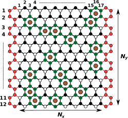
Fig.1 shows the geometry used for the calculations of charge and spin polarized conductances. Fig.1 is the setup corresponds to ZGNR. The length and width of these systems can be determined as shown in the given figure. In Fig.1, the width is, and the length is, . Thus we can denote the zigzag setup by Z-A 17Z-12A. This nomenclature for denoting the dimensions of the nanoribbon will be followed throughout the paper.
The black and white circles stand for the A and B sublattices of graphene. The brown circles are the magnetic adatoms. The green circles are the affected site due to magnetic adatoms. The black lines surrounding the adatoms correspond to the nearest neighbour hopping and the Rashba SOC. Rest of the black lines denote only nearest neighbour hopping. The leads are semi-infinite in nature, attached at both ends and are denoted by red color. The leads are considered to describes by a pure tight binding graphene lattice and hence are free of any kind of SOC.
II.2 Four terminal (4T) GNR: formulation of longitudinal and spin Hall conductances
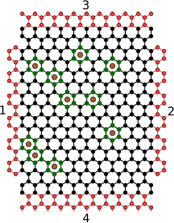
In order to observe the spin Hall conductance, a charge current is allowed to flow between terminal 1 and 2, and a spin current is observed to flow along the transferred direction of the rectangular sample, that is between terminals 3 and 4 as shown in Fig.2.
In case of four terminal device, the longitudinal and spin Hall conductances are defined as follows,
| (7) |
where, is the charge current flowing through terminal 2 and is the spin current polarized in a particular direction and flowing through terminal 3. is the potential at the -th lead.
Following the Landauer-Büttiker formula land_cond ; land_cond2 , the charge and spin currents can be calculated from the following expression chang ; roche ,
| (8) |
where, . is a identity matrix and are the Pauli matrices. in Eq.8 gives the usual charge current, while the Pauli matrices yield the spin currents polarized in different directions (, and ).
Since leads 3 and 4 are voltage probes, . On the other hand, as the currents in various leads depend only on voltage differences among them, we can set one of the voltages to zero without any loss of generality. Here we set .
III Results and Discussions
We have studied the charge and spin conductance properties in ZGNR decorated by magnetic adatoms and compared the results for two and four terminal devices.
Before embarking on the results, we briefly describe the values of different parameters used in our calculation. We set the hopping term, eV. Throughout our work, we take the ZGNR setup as 89Z-48A for the two terminal case. While for the four terminal device it is 85Z-52A. All the energies are measured in unit of . The charge conductance is measured in units of and the spin polarized conductance is measured in units of for the 2T case. The longitudinal and spin Hall conductances are measured in units of and respectively for the 4T case. Also the lattice constant, is taken to be unity. All the measurable quantities are averaged over 50 independent random-adatom configurations for different adatom concentrations, . In this work, we have considered three different adatom concentrations, namely, and . We have checked that 50 configurations are adequate in the present context, especially, since the adatom densities considered here are small. For most of our numerical calculations we have used KWANT kwant .
III.1 Two terminal
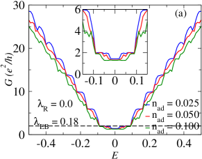
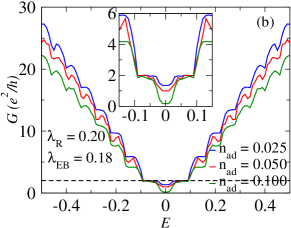
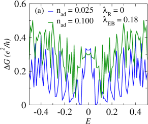
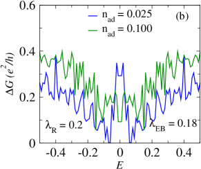
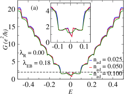
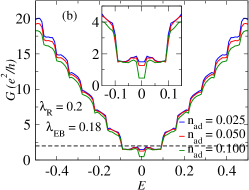
The behaviour of charge conductance, for two terminal case is studied as a function of the Fermi energy, as shown in Fig.3 for two different cases, in Fig.3(a) and in Fig.3(b). The strength of the exchange field is kept fixed at . Corresponding to these parameters, the insulating bulk states are clearly discernible from the chiral conducting edge states jiang . The variation of as a function of the Fermi energy is quite similar for two different strengths of the Rashba SOI. is symmetric around the zero of the Fermi energy and shows a nice necklace-type pattern for both the case. However, the behaviour of close to zero of the Fermi energy is different for the two different values of . In order to visualize the behaviour of close to zero of the Fermi energy, we plot for a small range of the Fermi energy as shown in the inset in Fig.3. In the absence of Rashba SOI, always stays finite. On the other hand, in presence of Rashba SOI, tends to vanish values in the vicinity of as we increase the adatom concentration. It identically vanishes at . The plateau in pristine graphene in presence of Rashba SOI is believed to be a signature of the quantum spin Hall insulating phase protected by the time reversal symmetry. In presence of the exchange bias, the time reversal symmetry is explicitly violated leading to the disappearance of the plateau and giving rise to features of an ordinary insulator.
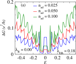
We did not show the fluctuations in the charge conductance in Fig.3 in order to avoid cluttering of data. However, the fluctuations in the charge conductance, is plotted as a function of the Fermi energy separately as shown in Fig.4 for clarity. Fig.4(a) shows the variation of in the absence of Rashba SOI and Fig.4(b) for a Rashba strength, . In both cases, fluctuations increases with increasing the adatom concentration. Rashba SOI suppresses the fluctuations in the charge conductance as seen from Fig.4(b). The spike-like behaviour in is due to the finite number of open channels in the leads and may be due to the spin precision effect sudin ; lsheng . For clarity, we have taken only two different adatom concentrations, namely 0.025 (denoted by blue color) and 0.1 (denoted by green color).
It is expected that in the absence of Rashba SOI, the exchange field generates only the -component of the spin polarized conductance, since the exchange field contains only the -component of the Pauli spin matrix (see Eq.1). However, the inclusion of the Rashba SOI generates all the three components of the spin polarized components.
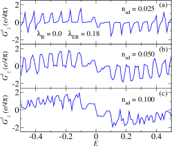
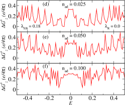
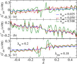
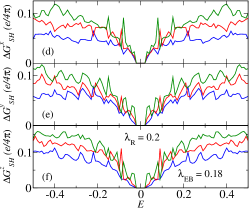
Fig.5(a-c) shows the variation of the -component of the spin polarized component, (in units of ) as a function of the Fermi energy, in the absence of Rashba SOI for three different adatom concentrations. is antisymmetric as a function of the Fermi energy owing to the electron-hole symmetry chico ; moca . Though we consider very dilute adatom concentrations, acquires quite a large value in the absence of Rashba SOI. The spike-like nature as discussed before is due to the finite number of open channels in the leads. The fluctuations in denoted by is plotted as a function of the Fermi energy, as shown in Fig.5(d-f). is symmetric about . However, in the absence of Rashba SOI, is more or less independent of the adatom concentration.
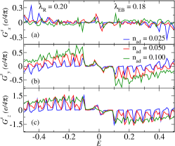
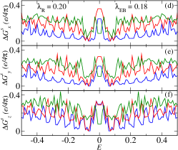
The behaviour of all the three components of spin polarized conductance as a function of in presence of Rashba SOI is plotted in Fig.6(a-c). The magnitude of the spin polarized conductance increases with increasing the adatom concentration. The -component, namely has a higher magnitude than the other two components of the spin polarized conductance. However, all of them are antisymmetric about as they should be. The magnitude of in presence of Rashba SOI is lower than the values corresponding to that of in the absence of Rashba SOI. The spike-like feature is mostly prominent in the behaviour of and a little in . The behaviour of the corresponding fluctuations in the spin polarized conductance is shown in Fig.6(d-f). As the adatom concentration is increased, the fluctuations also increase. But the most interesting feature about the fluctuations is that all the three components, that is have a unique behaviour as elaborated in the following. Even if the different components of the spin polarized conductance have different variations as a function of and have different orders of magnitude for a particular strength of the exchange field in presence of Rashba SOI, yet the orders of magnitude of their fluctuations are almost same. Further, as usual the fluctuations increases with increasing adatom concentration.
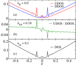
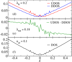
The inclusion of magnetic adatoms generates the exchange field and as a result, the time reversal symmetry is broken. Hence the system will no longer have a Kramer’s doublet. This phenomena can be justified through the density of states (DOS) for different species, that is DOS for up and down spins. We denote the total density of states by DOS, the density of states coming from spin up electron by UDOS and that from spin down electron by DDOS. We also define the difference between the UDOS and DDOS by DiffDOS.
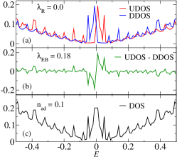
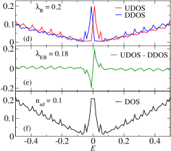
The variation of the DOS as a function of the Fermi energy is hence plotted in Fig.7 for a particular strength of the exchange field, . Fig.7(a) shows the behaviour of UDOS and DDOS in the absence of Rashba SOI and Fig.7(d) in presence of Rashba SOI. It is observed that UDOS is antisymmetric with respect to DDOS as a function of the Fermi energy. The difference between UDOS and DDOS, that is DiffDOS is plotted in Fig.7(b) and Fig.7(e) in the absence and presence of Rashba SOI respectively. In both cases UDOS DDOS is antisymmetric about . The total DOS, that is the sum of DOS due to spin up and spin down electrons is plotted in Fig.7(c) and Fig.7(f). DOS is symmetric about .
We can summarize the observations noted from the DOS data, as shown by the following set of properties,
| (9) | |||||
In order to have a deeper look, we have also shown the local charge and spin currents for a fixed Fermi energy. Since the left lead acts as an input to the system, we are interested in the local charge and spin currents which have originated due to the left lead.
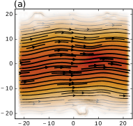
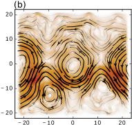
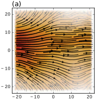
Fig.8(a) shows the nature of the local charge current, in the absence of Rashba SOI for a fixed value of the Fermi energy, namely . Clearly the local charge current is flowing between the left to the right lead without any distortion. In case of spin currents, there are three components, namely . Since in the absence of Rashba SOI only -component of the local spin current exits, we have calculated as shown in Fig.8(b). The number of paths between left and right leads are less compared to the local charge current. Few of the paths are even circling around certain points signaling a vortex like behaviour.
Since the inclusion of Rashba SOI generates the two other components of the spin polarized conductance, namely the and components, it will be meaningful to study the local spin currents of these components. Existence of all of these components should be beneficial for spintronic applications of magnetic adatom decorated GNRs.
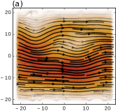
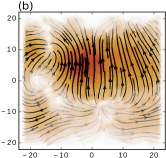
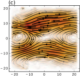
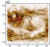
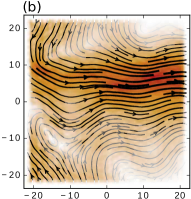
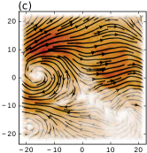
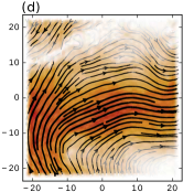
For this, we set, as before, the strength of the Rashba SOI at and fixed the energy at . The local charge and spin currents are shown in Fig.9. The local charge current, is again flowing between left and right leads as shown in Fig.9(a), which reveals that is almost independent of the Rashba SOI which is understandable. Fig.9(b),(c) and (d) show respectively , and . If we recall Fig.6, where are plotted as a function of the Fermi energy, the -component of the spin polarized conductance has the lower magnitude compared to the other two components. This can be explained from Fig.9(b). Here we see that the number of clear paths between left and right leads are very less compared to the paths corresponding to and . As a result, has lesser magnitude than and .
III.2 Four terminal
Having emphasized upon the conductance characteristics of a 2T GNR, it is useful to compare and contrast with respect to the 4T devices.
To begin with the results in case of four terminal device, we shall remind ourselves that the setup for measuring the longitudinal conductance and spin Hall conductance . As shown in Fig.2, an electric current is allowed to pass between terminal 1 and 2, and the longitudinal conductance is measured. Terminals 3 and 4 are the voltage probes, hence there will be no charge current flowing through them. The spin Hall conductance is measured between terminals 3 and 4.
The behaviour of the charge conductance, for a 4T case is studied as a function of the Fermi energy () as shown in Fig.10 for two different cases as earlier, namely, in Fig.10(a) and in Fig.10(b). The strength of the exchange field is kept fixed as in case of two terminal case, that is at . is symmetric around the zero of the Fermi energy and shows a nice necklace-type pattern for both the case. However, the behaviour of close to zero of the Fermi energy is different for two different values of . We plot for a small range of the Fermi energy in the vicinity of as shown in the inset in Fig.10. In the absence of Rashba SOI, always remain non-zero. On the other hand, in presence of Rashba SOI, tends to have lower values near as we increase the adatom concentration. One can expect an insulating behaviour about in presence of Rashba SOI if we increase the adatom concentration beyond . There is a crucial difference between the 2T and 4T devices with regard to the plateau at in the vicinity of the zero of the Fermi energy implying the existence of a quantum spin Hall phase. As discussed earlier, there is a fairly flat plateau for a 2T GNR without magnetic adatoms, which is visibly absent for a 4T GNR (see Fig.10 and the insets). This is another minor, where in a 2T device, we have observed to completely vanish at , while in the 4T GNR, it would eventually vanish for .
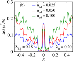
The fluctuations in the charge conductance, is plotted in Fig.11(a) in the absence of Rashba SOI and in Fig.11(b) in presence of Rashba SOI. In each of the plots, falls off as we come close to , from either side of the band and again increases near . The fluctuations increases as we increase the adatom concentration. By comparison the two plots, we observe that the inclusion of Rashba SOI causes larger fluctuations than the corresponding case where Rashba SOI is absent.
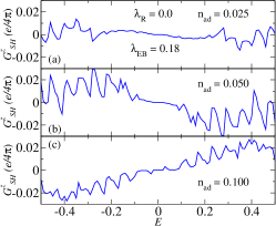
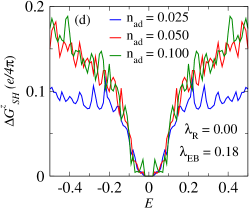
Same as that of the spin polarized conductance, the spin Hall conductance has also three components, namely , and . Since the and -component of the spin Hall conductance are absent in the absence of Rashba SOI, we have shown only the variation of in units of as a function of the Fermi energy as shown in Fig.12(a-c)and corresponding fluctuations in Fig.12(d).
is plotted for three different adatom concentrations separately for better clarity. The behaviour of is antisymmetric about and the magnitude (irrespective of the sign factor) increases as the adatom density is enhanced. The maximum values of are observed on either side of the zero of the Fermi energy and close to , the value decreases. The corresponding fluctuations are shown in a single plot in Fig.12(d). As expected, with increasing the adatom concentration, increases. Another important point to be noted here is that there is a finite region about the zero energy where and are strictly zero irrespective of the adatom concentration which is owing to the single channel transmission chico ; liu .
The effect of the inclusion of Rashba SOI on the three components of the spin Hall conductance is observed in Fig.13(a-c). All of them are antisymmetric about . Their magnitude increases with increasing the adatom concentration. Though the behaviour of the different components of the spin Hall conductance are different in nature as a function of the Fermi energy, their order of magnitude is similar. The fluctuations in the spin Hall conductance are plotted in Fig.13(d-f) as a function of the Fermi energy. as observed the case in the absence of Rashba SOI, in the present case, , and have similar variations with , that is they increase with increasing adatom concentration. further, their orders of magnitude are also same.
The DOS plots in the absence of Rashba SOI are shown in Fig.14(a-c) and in the presence of Rashba SOI in Fig.14(d-f). UDOS and DDOS are antisymmetric to each other as we have observed in case of two terminal case. the magnitude of UDOS and DDOS are higher at higher values of as shown in Fig.14(a) and Fig.14(d) and in both the cases, that is, in presence and absence of Rashba SOI, their magnitudes seem to be independent of the strength of Rashba SOI. The difference between UDOS and DDOS, DiffDOS (= UDOS - DDOS) is antisymmetric in nature as a function of the Fermi energy and has somewhat larger oscillatory behaviour in presence of RSOI than that in the absence of RSOI. Also the total DOS is symmetric about . Basically all the three quantities are in good agreement with Eq.III.1 both in the absence and presence of Rashba SOI.
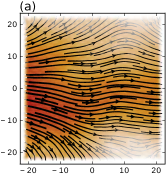
Finally, the local charge current and the -component of the local spin current are shown in Fig.15(a) and Fig.15(a) respectively in the absence of Rashba SOI. For the local charge current, it is observed that as though the transverse leads are voltage probes, the charge current is flowing between lead 1 and lead 3. In another word, the charges are trying to accumulate at the transverse edges of the sample and as a result less charge current flows between terminals 1 and 2. This in turn reduces the charge conductance in case of a 4T device than the 2T case. The -component of the local spin current is clearly flowing from terminals 1 to 3 and between terminal 1 to 4. As a result the non-zero occurs due to presence of the exchange field.
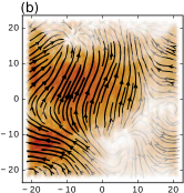
The local charge and spin currents are shown in Fig.16 in presence of Rashba SOI. The local charge current, flows between the left and right leads (terminals 1 and 2 respectively) as shown in Fig.16(a). We observe that is almost independent of the Rashba SOI. This explains why the charge conductance is independent of the Rashba SOI as shown in Fig.10(a) and Fig.10(b).
Fig.16(b), (c) and (d) show respectively local currents, namely , and . We observe that the magnitude of the -component of the spin Hall conductance (see Fig.12(a-c)) is one order magnitude lower than any one of the components of SHC in presence of Rashba SOI, which can be explained as following. From Fig.16(b-c), the number of paths between terminal 1 and either terminals 3 or 4 are more than the absence of Rashba SOI case as shown in Fig.15(b). As a result, the amount of spin current will be less in the absence of Rashba SOI.
IV Conclusion
In the present work we have studied the behaviour of the charge and spin transport properties in graphene nanoribbon with magnetic adsorbates both in case of two terminal and a four terminal GNR. Specifically for the two terminal case, we study the charge and spin polarized conductance and for the four terminal case the spin Hall conductance. In all the cases we found that the charge conductance is symmetric about the zero of the Fermi energy, while the spin polarized conductance (for two terminal case) and spin Hall conductance (for four terminal case) are antisymmetric about the zero of the Fermi energy.The fluctuations of the charge and spin conductances show systematic behaviour, that is they increase with increasing adatom concentration. We also study the DOS behaviour and their behaviour are alike in both two and four terminal cases. The local charge current is found to be independent of the strength of Rashba SOI, while the three different components of the local spin currents are sensitive to Rashba SOI that is generated by the magnetic adatoms. Further the -component of the spin polarized conductance for 2T GNR is larger by approximately a factor of 5 compared to its 4T counterpart, while the other two components are nearly same for the 2T and 4T devices. Of course a 4T device permits observations of a spin Hall conductance, which is absent in the case of a 2T GNR. Moreover the conductance properties of a 4T setup has lesser fluctuations.
The increase in the components of the spin polarized conductances in magnetic decorated GNRs with Rashba SOI signal a larger spin current flowing in the sample and hence must have greater utility as possible spintronic devices.
ACKNOWLEDGMENTS
SG gratefully acknowledges a research fellowship from MHRD, Govt. of India. SB thanks SERB, India for financial support under the grant F. No: EMR/2015/001039.
References
- (1) K. S. Novoselov, A. K. Geim, S. V. Morozov, D. Jiang, Y. Zhang, S. V. Dubonos, V. Grigoreva, and A. A. Firsov, Science 306, 666 (2004).
- (2) A. H. C. Neto, F. Guinea, N. M. R. Peres, K. S. Novoselov, A. K. Geim, Rev. Mod. Phys. 81, 109 (2009).
- (3) Y. Zhang, Y.-W. Tan, H. L. Stormer, and P. Kim, Nature 438, 201 (2005).
- (4) V. P. Gusynin and S. G. Sharapov, Phys. Rev. Lett. 95, 146801 (2005).
- (5) E-J. Kan, Z. Li, J. Yang and J. G. Hou, Appl. Phys. Lett. 91, 243116 (2007).
- (6) X. Lin and J. Ni, Phys. Rev. B 84, 075461 (2011).
- (7) X. Du, I. Skachko, A. Barker and E. Y. Andrei, Nat. Nanotech. 3 491 (2008).
- (8) J. C. Meyer, A. K. Geim, K. S. Novoselov, T. J. Booth, and S. Roth, Nature London 446 ,60 (2007).
- (9) S. V. Morozov, K. S. Novoselov, M. I. Katsnelson, F. Schedin, L. A. Ponomarenko, D. Jiang, and A. K. Geim, Phys. Rev. Lett. 97 , 016801 (2006).
- (10) K. Wakabayashi, M. Fujita, H. Ajiki and M. Sigrist, Phys. Rev. B 59, 8271 (1999).
- (11) R. Saito, M. Fujita, G. Dresselhaus, M.S. Dresselhaus, Appl. Phys. Lett. 60 , 2204 (1992)
- (12) K. Nakada, M. Fujita, G. Dresselhaus and M. S. Dresselhaus, Phys. Rev. B 54, 17954 (1996).
- (13) Z. F. Wang, Q. Li, H. Zheng, H. Ren, H. Su, Q. W. Shi and J. Chen Phys. Rev. B 75, 113406 (2007).
- (14) H. Zheng and W. Duley, Phys. Rev. B 78, 045421 (2008).
- (15) L. L. Song, X. H. Zheng, R. L. Wang and Z. Zeng, J. Phys. Chem. C 114, 12145 (2010).
- (16) H. Zeng, J. Zhao, J. W. Wei and H. F. Hu, Eur. Phys. J. B 79 , 335 (2011).
- (17) X. H. Zheng, L. L. Song, R. N. Wang, H. Hao, L. J. Guo and Z. Zeng, Appl. Phys. Lett. 97, 153129 (2010).
- (18) H. Zhang, S. Meng, H. Yang, Lin Li, H. Fu, Wei Ma, C. Niu, J. Sun and C. Gu, J. App. Phys. 117, 113902 (2015).
- (19) R. C. Longo, J. Carrete and L. J. Gallego, Phys. Rev. B 83, 235415 (2011).
- (20) K. T. Chan, J. B. Neaton and M. L. Cohen, Phys. Rev. B 77, 235430 (2008).
- (21) A. V. Krasheninnikov, P. O. Lehtinen, A. S. Foster, P. Pyykkö and R. M. Nieminen, Phys. Rev. Lett. 102, 126807 (2009).
- (22) D. W. Boukhvalov and M. I. Katsnelson, Appl. Phys. Lett. 95, 023109 (2009).
- (23) E. J. Kan, H. J. Xiang, J. Yang and J. G. Hou, J. Chem. Phys. 127, 164706 (2007).
- (24) H. Sevinçli, M. Topsakal, E. Durgun and S. Ciraci, Phys. Rev. B 77, 195434 (2008).
- (25) V. A. Rigo, T. B. Martins, A. J. R. da Silva, A. Fazzio and R. H. Miwa, Phys. Rev. B 79, 075435 (2009).
- (26) W. H. Brito and R. H. Miwa, Phys. Rev. B 82, 045417 (2010).
- (27) J. -F. Liu, K. S. Chan and J. Wang, Nanotechnology 23, 095201 (2012).
- (28) L. Chico, A. Latge and L. Brey, Phys. Chem. Chem. Phys. 17, 16469 (2015).
- (29) Q. Zhang, K. S. Chan and J. Li, Phys. Chem. Chem. Phys. 19, 6871 (2017).
- (30) P. Esquinazi, A. Setzer, R. Höhne, C. Semmelhack, Y. Kopelevich, D. Spemann, T. Butz, B. Kohlstrunk and M. Lösche, Phys. Rev. B 66, 024429 (2002).
- (31) R.C. Longo, J. Carrete, L.J. Gallego, J. Chem. Phys. 134, 024704 (2011).
- (32) E. J. G. Santos, A. Ayuela, and D. Sánchez-Portal, New J. Phys. 12, 053012(2010).
- (33) Y. Mao, J. Yuan and J. Zhong, J. Phys.: Condens. Matter 20, 115209 (2008).
- (34) C. Cao, M. Wu, J. Jiang, and H-P Cheng, Phys. Rev. B 81, 205424 (2010).
- (35) N. K. Jaiswal and P. Srivastava, Physica E 54, 103 (2013).
- (36) Z. Qiao, Shengyuan A. Yang, W. Feng, W-K Tse, J. Ding, Y. Yao, J. Wang, and Q. Niu, Phys. Rev. B 82, 161414(R) (2010).
- (37) R. Landauer, IBM J. Res. Dev. 1, 223 (1957).
- (38) R. Landauer, Philos. Mag. 21, 683 (1970).
- (39) C. Caroli, R. Combescot, P. Nozieres and D. Saint-James, J. Phys C: Solid State Phys. 4, 916, (1971).
- (40) D. S. Fisher and P. A. Lee, Phys. Rev. B 23, 6851 (1981).
- (41) S. Datta, Electronic transport in Mesoscopic systems, University press (Cambridge), (1995).
- (42) B. K. Nikolić, Phys. Rev. B 64, 014203 (2001).
- (43) A. Cresti, B. K. Nikolić, J. H. García and S. Roche, Rivista Del Nuovo Cimento 39, 12 (2016).
- (44) P.-H. Chang, F. Mahfouzi, N. Nagaosa and B. K. Nikolic, Phys. Rev. B 89, 195418 (2014).
- (45) C. W. Groth, M. Wimmer, A. R. Akhmerov, X. Waintal, Kwant: a software package for quantum transport, New J. Phys. 16, 063065 (2014).
- (46) S. Ganguly and S. Basu, Physica E 90, 131 (2017).
- (47) L. Sheng, C.S. Ting, Physica E 33, 1 (2006).
- (48) C. P. Moca and D. C. Marinescu, Phys. Rev. B 72, 165335 (2005).