Quantum fluctuations of the current in a tunnel junction at optical frequencies
Abstract
We have investigated the mechanism at the origin of the infra-red radiation emitted by a biased tunnel junction by detecting photons at frequencies . To address this regime, the bias voltage exceeds one volt and the potential profile of the tunnel barrier is driven far from its equilibrium state. As a consequence, the characteristic of the junction is strongly nonlinear. At optical frequencies, the transport through the junction cannot be simply expressed in term of the dc current and the current fluctuations are no longer described by the fluctuation-dissipation relation. Taking into account the energy and voltage dependence of the transmission of the tunnel junction in a Landauer-Büttiker scattering approach, we experimentally demonstrate that the photon emission results from the fluctuations of the current inside the tunneling barrier.
pacs:
72.70.+m, 42.50.Lc, 42.50.Ct, 73.23.-b, 73.20.MfFluctuations of the current in a conductor give rise to electromagnetic radiation. In the free space at thermal equilibrium, the radiated spectral power is described by Planck’s law and is a direct consequence of the fluctuation-dissipation theorem (FDT): the thermal fluctuating currents in the conductor generate an electromagnetic field related to the dissipation in the conductor through its resistivity Nyquist (1928); Callen and Welton (1951). Besides thermal fluctuations, conductors can experience another fundamental source of current fluctuations, the so-called shot noise. A natural question arise : can the black-body law be generalized to current-biased conductors? If such a generalization exists, it should particularly be observed in conductors exhibiting Poissonian shot noise like tunnel junctions. Even though broadband light emitted from metallic tunnel junctions was first observed in the late 70’s by Lamb and McCarthy Lambe and McCarthy (1976), no general relation has been established so far between the emission spectrum at optical frequencies and the electronic transport through the junction Kirtley et al. (1981); Hanisch and Otto (1994). Following the Nyquist argument Nyquist (1928), the radiated spectral power emitted by a planar tunnel junction can be expressed in terms of the current noise spectral density and a radiation impedance standing for the coupling between the tunneling currents in the conductor and the far field radiating electromagnetic modes:
| (1) |
In the case of a tunnel junction at thermal equilibrium, the FDT gives where denotes the Bose-Einstein distribution and the dc conductance of the junction. For a dc-polarized tunnel junction, the FDT has been generalized to an expression which is usually referred to as a fluctuation dissipation relation (FDR) Rogovin and Scalapino (1974); Lee and Levitov (1996); Sukhorukov et al. (2001); Roussel et al. (2016):
| (2) |
where is the dc characteristic of the voltage-biased tunnel junction. This prediction is in quantitative agreement with experiments in the microwave regime in a linear tunnel junction Basset et al. (2010); Gabelli and Reulet (2008) or in a tunnel junction showing non-linear features of dynamical Coulomb blockade Parlavecchio et al. (2015). Although this FDR is universal at zero frequency and can be deduced from a general fluctuation theorem SM ; Evans et al. (1993); Esposito et al. (2007), we show in this letter that it breaks down at optical frequencies (). Eq. (2) is indeed based on a perturbation theory applied to a model transfer Hamiltonian Bardeen (1961); Roussel et al. (2016) and cannot stand when the bias voltage is comparable with the tunneling barrier height. First, the tunneling barrier is modified by the bias voltage leading to an intrinsic non-linearity conductance. Second, the spectral noise density measured at optical frequencies probes current correlations on a time scale on the order of the time for an electron to cross the barrier SM ; Büttiker and Landauer (1982). The photon emission is then a “snapshot” of the tunneling event and requires a microscopic description of the charge transfer inside the tunneling barrier. Our experiments not only shed light on the origin of light emission by tunnel junctions, but also extend the concepts of low-energy electronic transport to a few and explore the new regime of finite frequency quantum noise in nonlinear transport. The letter is organized as follows: (i) we define the transport in a tunnel junction in the far-from-equilibrium regime (FFER). (ii) We describe the experimental setup (FIG. 1). (iii) We experimentally show that the FDR holds on in the FFER at zero frequency proving the validity of the tunneling limit. (iv) We use a Landauer-Büttiker (LB) approach based on elastic tunneling processes to quantitatively describe the noise spectral density in the optical spectral range.
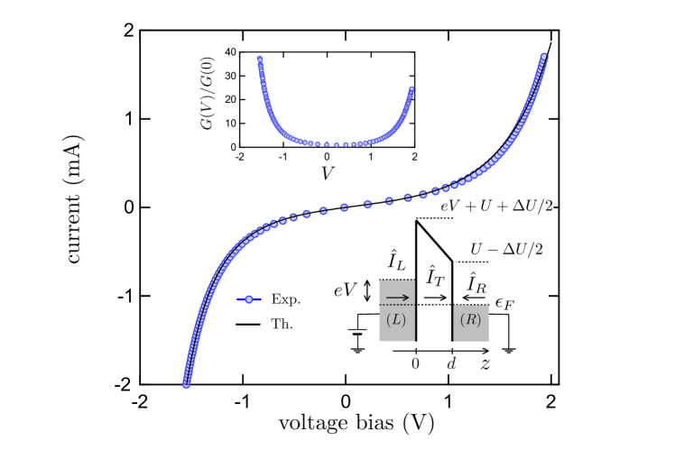
Nonlinear tunneling transport. The FFER is achieved when the applied bias voltage is of the order of the tunnel barrier height . In this regime, without a careful study of the Coulomb interactions in the tunnel barrier, gauge invariance (invariance of the current under a global voltage shift applied on both electrodes) is not systematically satisfied Christen and Büttiker (1996); Blanter and Büttiker (2000). It is indeed necessary to determine the electrical potential which depends on the applied bias voltage and the possible charge accumulation in the conductor. The transmission of the barrier is thus necessarily energy and voltage dependent and the characteristic is expressed according to the Landauer-Büttiker formula as:
| (3) |
where is the Fermi-Dirac distribution with the Fermi energy. In the tunneling limit, the voltage dependence of can be deduced from the Wentzel-Kramers-Brillouin (WKB) approximation by considering a total potential including the potential barrier and the biasing energy as depicted in FIG. 2Simmons (1964). It is worth emphasizing that the biasing energy is essential to explain non-symmetric characteristics as shown in FIG. 2. We now consider the current fluctuations characterized by the non-symmetrized spectral noise density where is the Fourier component of the current operator measured in the electrode and the measurement bandwidth. For , this quantity refers to the emission quantum noise which is measured in a passive detection scheme such as the photon detector used here Lesovik and Loosen (1997); Blanter and Büttiker (2000). Using the scattering LB approach for a single quantum channel of conduction in the tunneling limit (), we get for Blanter and Büttiker (2000):
| (4a) | ||||
| (4b) | ||||
where and . In the zero-frequency limit, a straightforward calculation leads to and the FDR holds even in the nonlinear regime. However, at finite frequency, the energy dependence of the transmission leads to a charge accumulation in the barrier and the noise spectral density depends on the electrode where it is evaluated () Blanter and Büttiker (2000); Zamoum et al. (2016). Because of the screening of the electromagnetic field in the metallic electrodes, the coupling is expected to be dominant in the insulating barrier and requires the determination of the tunneling current to evaluate the radiation impedance. Although it should be necessary to solve the coupled system of Schrödinger and Poisson equations to calculate the tunneling current , the screening in metallic electrodes enables a simple description of . The bare electron inside the tunneling barrier induces a polarization charge and in the left and right electrodes respectively (see FIG. 2). We can thus assume that the charge accumulation on the surface of the electrodes is equal in average during the tunneling event: with . The continuity equation then implies with the conventional direction of the current (FIG. 1(c)) Lü et al. (2013). The current noise spectral density in Eq. (1) is then given by:
| (5) |
while the radiation impedance is associated with the leakage of the surface plasmon polariton (SPP) mode in the substrate (FIG 1(c)). Under these conditions, the FDR cannot be satisfied anymore and the radiated spectral power measured by the photon detector is a linear combination of , and given by the coupling between the current fluctuations and the electric field in the junction. It should be stressed that the expression of account for all the effects of Coulomb interactions.
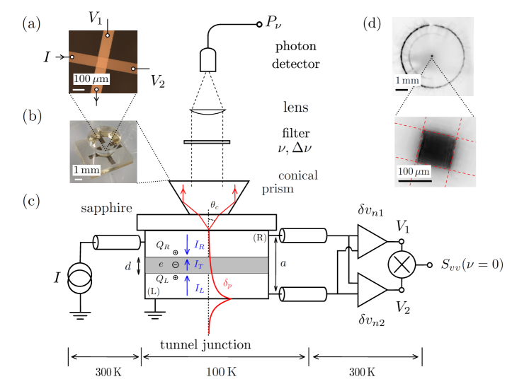
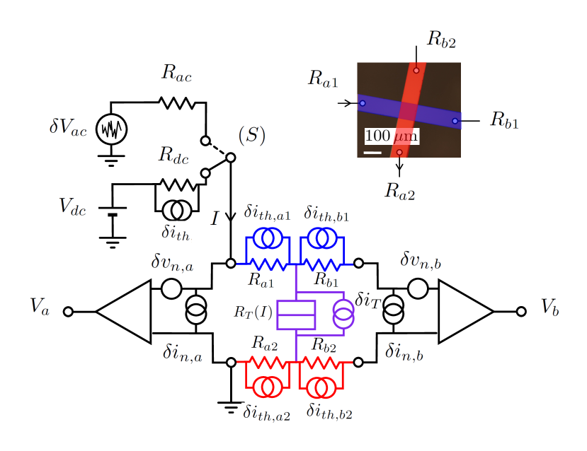
Experimental setup. Our experimental setup is shown in FIG. 1. Electronic and optical measurements are performed in a cryogenic environment at to prevent junction breakdown and to reduce the thermal noise on the infrared photon-detector. The sample is a planar tunnel junction deposited on a sapphire substrate (FIG. 1(a)). Because of the layered structure of the junction, the electromagnetic modes are localized in the junction and consequently should not radiate in the free space. However, the total thickness of the junction is smaller than the penetration depth of the SPP in the metal: with the plasma frequency of aluminum. It then allows the coupling between the SPP mode localized at the interface electrode/vacuum (FIG 1(c)) and the propagating mode in the substrate SM . This corresponds to the Kretschmann configuration where the coupling appears at a specific angle where stands for the refractive index of sapphire Kretschmann (1972). We use total internal reflection in a conical prism to collect the emitted photons (see FIG. 1(b,c)). The current noise at optical frequency is measured at two different frequencies corresponding to the wavelengths and . The current noise at zero frequency is measured with a standard cross-correlation technique SM .
Electrical properties - Noise measurement at zero frequency. At high voltage the characteristic shown in FIG. 2 exhibits a strong nonlinearity: the differential resistance varies by more than one order of magnitude going from at low bias to at high bias. From the theoretical expectation of Eq. (3) using the WKB approximation to evaluate the transmission of the tunnel junction, we estimate the mean barrier height , its asymmetry and its thickness (lower inset of FIG. 2). The thickness is in agreement with the capacitance of the junction .
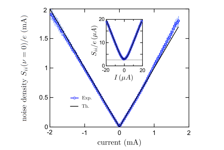
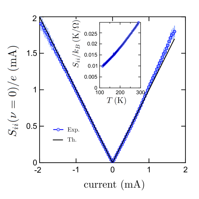
Current fluctuations at zero frequency are measured with low noise voltage amplifiers giving access to voltage fluctuation where is the global gain of the amplifier chain, is the transimpedance of the measurement setup and its excess noise. Because of the large variation of the tunneling resistance, a careful calibration is required to extract the current noise . The voltage-dependent transimpedance and the excess noise are determined by using an external noise source while is deduced from the measurement of the shot noise in the linear regime SM . FIG. 3 shows the current noise in the FFER. Although the tunnel resistance is strongly nonlinear, clearly satisfies the FDR at zero frequency:
| (6) |
In the high bias limit , the current noise is then linearly proportional to the dc current which is a signature of shot noise. It confirms that electronic transport through the junction operates in the tunneling limit at high voltage bias ruling out the presence of pinholes in the barrier. We notice systematic errors at high positive bias. They cannot be attributed to Joule heating since they should also be observed for negative bias. The fact that calibration is off by is attributed to parasitic capacitances of the measurement setup which are not included in .
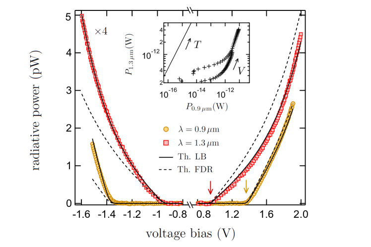
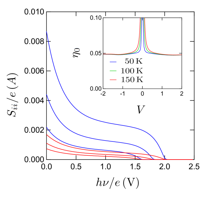
Light emission - Noise measurement at optical frequency. FIG. 1(d) shows an image of the light emission pattern from the tunnel junction when the camera is focused on the conical prism. In the center, a small amount of light comes directly from the tunnel junction (zoom in FIG. 1(d)). This is due to surface roughness of electrodes allowing SPP scattering at the surface of the upper electrode Hanisch and Otto (1994). The homogenous light intensity indicates that electron to photon conversion in the tunnel junction is also homogenous over the surface of the junction. However, the bright ring in FIG. 1(d) reveals that more than of the light is emitted at the specific angle as expected in the Kretschmann configuration. The light power is plotted as a function of the voltage bias for two different wavelengths in FIG. 4. Inset of FIG. 4 displays the relationship between the light power at the two wavelengths on a log-log plot Bonnet and Gabelli (2010). Data points do not fit the black-body radiation law (solid line in inset) and, as previously mentioned, the Joule heating cannot be responsible for the observed photon emission. The light power exhibits a voltage cross-over at : electrons crossing the tunnel junction relax their energy by emitting photons at frequency . This cross-over is predicted both by the FDR and the LB theories. However, our data clearly disagree with the FDR (dashed line in FIG. 4) and are in very good agreement with the LB relation of Eq. (5) (solid line in FIG. 4). The LB approach enables us to understand the dependence on the bias polarity of the light emission which has already been observed but not explained Kirtley et al. (1981, 1983); Hanisch and Otto (1994). It also allows one to extract the radiation impedance according to Eq. (1). This gives and about a factor four higher than our rough estimation in the limit Laks and Mills (1979); Ushioda et al. (1986):
| (7) |
where , , is the refractive index of sapphire and the alumina dielectric barrier, is the thickness of the barrier and is the vacuum impedance. This under-estimation can be attributed to the approximative values of the thickness and the refractive index of the dielectric barrier but also to the interband transition at in aluminum. We assume here that the coupling between the current fluctuations and the electric field takes place in the insulating barrier. This is justified by the screening of the electric field in the metal. If we only consider the coupling in the electrodes, we indeed expect a radiation impedance in the range, three orders of magnitude smaller than the observed one SM . However, the radiation impedance in the range is rather small and appears as a central quantity in the understanding of the small emission light efficiency of tunnel junctions. This lead us to redefine the efficiency with respect to the dissipated Joule power: . According to this definition, we can show that the efficiency is now directly related to the radiation impedance: where is the quantum of resistance and is a constant slightly dependent on the details of the barrier SM . We emphasize that this definition contrasts with the usual one which is given by the electron-to-photon conversion rate. We find the former more appropriate since it reflects the fact that, in metallic tunnel junctions, electrons with energy smaller than bias voltage can contribute to the current. In fact, unlike semiconductors, the lack of a band gap in metals indeed implies that each electron crossing the barrier emits a bunch of photons in a spectral range with a radiated spectral power proportional to the current. The emitted light power is then proportional to the Joule power .
Discission. The photon emission in a tunnel junction is usually attributed to the spontaneous emission in the barrier by inelastic electron tunneling Persson and Baratoff (1992); Berndt et al. (1991); Parzefall et al. (2015). However, it is worth noting that the LB approach which is used here only describes elastic tunneling processes. In this description, the energy relaxation formally takes place in the electrodes and corresponds to electron-hole pair recombinations specified by , and Zamoum et al. (2016). Nevertheless, by considering the coupling to the electric field only in the dielectric layer, we implicitly assume a relaxation in the tunneling barrier associated to the noise spectral density and our approach is not in contradiction with the inelastic interpretation. We actually use the elastic tunneling current to calculate the radiation impedance neglecting the feedback of the electromagnetic environment on the current fluctuations. This feedback, called the dynamical Coulomb blockade, is responsible for inelastic tunneling processes but is negligible here since Xu et al. (2014); Altimiras et al. (2016).
We have measured the current fluctuations in a metallic tunnel junction in the optical domain. In this regime, cannot be described anymore with a usual fluctuation dissipation relation because of the energy and voltage dependance of the tunneling transmission. We have shown how this dependence can be incorporated into the Landauer-Büttiker formalism to ensure the gauge invariance of the characteristic in the far-from-equilibrium regime and describe the quantum fluctuations of the current at optical frequencies. This theoretical description is in good agreement with our experimental results and sheds light on the estimation of quantum efficiency of metallic tunnel junction as a light emitter. Our experimental approach demonstrates that optical measurements are a powerful tool to study the quantum electronic transport at high energy () and extend the range of applicability of conventional concepts of mesoscopic electronic transport. Establishing a new fluctuation dissipation relation in the optical regime will require a properly defined response function of the tunneling current at optical frequencies.
Acknowledgements. We acknowledge fruitful discussions with E. Akkermans, M. Aprili, J. Basset, E. Boer-Duchemin, J. Estève, J-J Greffet, B. Reulet, E. Pinsolle I. Safi and P. Simon. We also thank A. Crépieux for useful insight. This work was supported by ANR-11-JS04-006-01, Investissements d’Avenir LabEx PALM (ANR-10-LABX-0039-PALM) and ANR-15-CE24-0020.
Supplemental Material
This supplemental material provides details on (I) the experimental setup, (II) the calibration procedure used to extract the current shot noise in the zero frequency limit, (III) the Landau-Büttiker formalism used to describe the current noise in the tunnel junction in the far-from-equilibrium regime (FFER), (IV) the validity of the fluctuation-dissipation relation (FDR) and (V) the Laks-Mills theory used to derive the radiation impedance.
I Sample fabrication and experimental setup
The sample is a planar aluminum tunnel junction deposited on a sapphire substrate. Numbers stand for the thickness in nm. The junction is fabricated by thin film deposition through shadow masks in a typical base pressure of with an oxidation of the first electrode in an oxygen glow discharge. The Kretschmann configuration is realized by using a glass prism Kretschmann (1972). The characteristic is measured using a standard four points technique with a dc voltmeter whereas the bias-dependence of the tunneling conductance is measured using a standard lock-in technique. The current noise in the zero frequency limit is measured using a cross-correlation technique and a real time FFT-based spectral measurement performed with a digitizer. Radiated power at wavelength is measured with filtered Si (at ) and InGaAs (at ) amplified detectors and a lock-in technique by modulating the voltage bias at . Their noise equivalent power are and respectively. To collect as much light as possible, the emitted light is refracted on a conical prism then collimated on the photon detector by using an aspherical lens (focal length , numerical aperture ). The detection efficiency is estimated at .
II Calibration of the shot noise measurement setup
The current noise in the zero frequency limit is measured using a cross-correlation technique to remove the amplifier voltage noise (). If the current noise () can be neglected, the thermal noise of the contact resistances in series with the tunnel junction has to be subtracted. The resistance of the thin electrodes () are indeed of the same order of magnitude than the differential tunnel resistance at high voltage bias: , , , (see inset of FIG. 5). The voltage noise measured by the experimental set up depicted in FIG. 5 is:
| (8) |
where is the global gain of the amplifier chain, is the transimpedance and the excess noise related to the measurement setup. FIG. 6 shows the voltage noise spectral density measured in the frequency range . It cannot be directly compared to the current noise spectral density of the tunneling current because of the voltage dependence of . A white voltage noise source is then used to calibrate the detection setup. If is high enough to neglect the intrinsic noise of the junction, the measured voltage noise enables to determine and :
| (9a) | ||||
| (9b) | ||||
where , , , and is the temperature of electrons. FIG. 7 shows the current shot noise and the theoretical expectation given by the FDR. The thermal noise measured at zero voltage bias for different temperature is shown on the inset of FIG. 7 and is in good agreement with the fluctuation-dissipation theorem . Note the typical temperature dependence of the tunneling junction resistance which increases when the temperature decrease Patiño and Kelkar (2015). As mentioned in the article, the Joule heating () cannot explain the discrepancy between the data and the theory. The electron-phonon coupling for gives a thermal conductance which leads to an electronic temperature equals to the temperature of the lattice such as: Lin et al. (2008). One indeed deduces that the temperature of electrons is homogeneous over the whole sample.
III Electronic transport in a tunnel junction in the far from equilibrium regime
III.1 Energy and voltage dependence of the transmission - characteristics
We consider a tunnel junction with the surface area and a large number of transverse channels labeled by the wave vector . We assume that electrons are scattered elastically on the tunneling barrier without any inelastic energy loss inside the barrier. The tunnel current is then given by the Landauer-Büttiker formula:
| (10) |
where is the Fermi-Dirac distribution, the Fermi energy and the transmission probability for an incoming electron with a transverse wave vector and a total energy . To recover the expression of Eq. (3) in the article, we define the transmission the transmission for an incoming electron with a total energy by averaging the WKB transmission over all possible values of Simmons (1964); Hansen and Brandbyge (2004):
| (11) |
where is the Wentzel-Kramers-Brillouin (WKB) transmission coefficient through a 1D potential barrier , is the thickness of the barrier and is the number of transversal modes of conduction contained in the tunnel junction area :
We are considering here the total potential including the potential barrier and the biasing energy . The biasing energy considers only the energy of the tunneling electron in the uniform electric field induced by the bias voltage, we have implicitly neglected the effects of space charge inside the barrier and image charge in the electrodes. In aluminum, the Fermi energy is and the Fermi wavelength . Then, the number of channels in the tunnel junction is and the transmission in the considered voltage range is . The asymmetry of the trapezoidal barrier is obtained with the second order expansion of the normalized conductance Brinkman et al. (1970):
| (12) |
with . The parabolic fit of data in the inset of Fig. 6 gives and . We then deduce . The values of and are estimated from the fit of the characteristics. These values are obtained by considering the effective mass of electrons in the oxide () Zemanová Diešková et al. (2013). We have checked that the charging effects in the barrier slightly change and of about . The large value of the asymmetry can be attributed to the growth on different substrates (/). One has to keep in mind that the trapezoidal barrier model is a simplistic model which cannot fully describe our sample. The effects of image charge could be considered in the potential barrier , they would only re-normalized the barrier height. They will be taken into account only to estimate the tunneling current. The capacitance of the tunnel junction is measured thanks to the cut-off frequency observed on the noise spectral density at low bias voltage. This value is in agreement with the thickness of the tunnel barrier: where is the dielectric constant of alumina, is the vacuum permittivity and the surface of the junction.
III.2 Gauge invariance
The gauge transformation corresponds to the addition of a constant potential on both electrodes. It leads to the following transformations: for the biasing energy, for the WKB transmission coefficient and and for the Fermi-Dirac distributions in the electrodes. It is straightforward to check that Eq (3)(4a)-(4c) in the article are invariant under these transformations.
III.3 Current noise spectral density at finite frequency
At zero frequency, the current noise spectral density is given by the fluctuation dissipation theorem where denotes the Bose-Einstein distribution and the dc conductance of the junction. Note that the absorption is due to the tunnel resistance and not to the resistance of the electrodes which are assumed negligible compared to the resistance of junction. However, as it has been shown in the article, the noise spectral density depends on the electrode where it is evaluated because of the energy and voltage dependent transmission (). It should also be stressed that, if we only consider the energy dependence of the transmission and omit its voltage dependence, the gauge invariance is violated and only one of the correlators satisfies the FDR, according to our choice of voltage biasing. For a 3D tunnel junction, Eq. (4c) in the article has to be slightly modified to take into account the summation over the transversal modes:
| (13) |
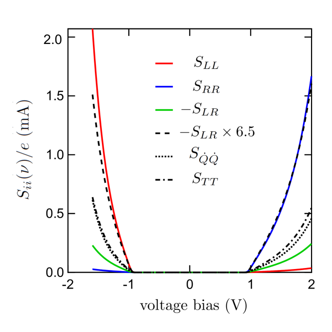
whereas Eqs. (4a) and (4b) remain unchanged considering the transmission given by Eq. (11). FIG. 8 shows the theoretical noise spectral density , and at using the parameters of the junction. and exhibit a strong dissymmetry revealing that energy relaxation occurs essentially in the left (resp. right) electrode for (resp. ) and can be interpreted as an electron-hole pairs recombination in the left (resp. right) electrode Zamoum et al. (2016). is more difficult to interpret and appears as an interference between the two former processes. Note that is almost proportional to (resp. ) for (resp. ). It implies, because of the strong asymmetry, with a factor of proportionality depending on the frequency (see Fig. 8). The tunneling current is assumed to be constant in the barrier and given by the average current . The tunneling current spectral noise density is then:
| (14) |
Although photon emission is due to the coupling to the fluctuations of the tunneling current , we can compare this quantity to the fluctuations of the accumulated charges on the electrodes of the junction related to :
| (15) |
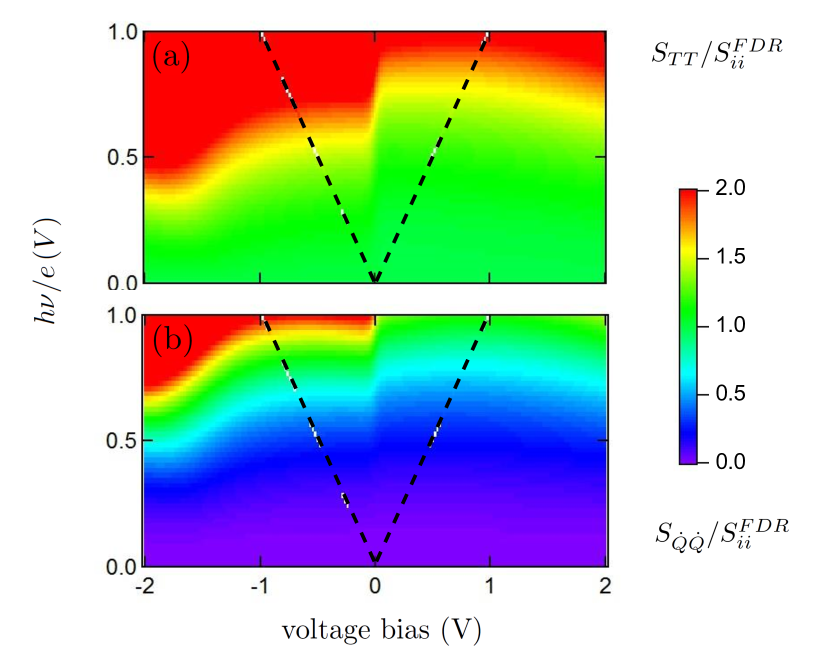
FIG. 8 and FIG. 9 show a significant difference between and . We also notice that at zero frequency. The experimental data presented in the article in Fig. 4 falls on and are not in agreement with .
III.4 Traversal time in a tunnel junction
The time for an electron to cross the barrier is defined as the traversal time where is the barrier height, its thickness, the effective mass of electron and the bias voltage. For a common aluminum oxide barrier , and which gives at Büttiker and Landauer (1982). This time is comparable to the time scale probed by the spectral noise density at optical frequencies. It is also comparable to the average time between electrons emitted between the two voltage biased electrodes which gives at Thibault et al. (2015).
IV Fluctuation-dissipation relation at zero frequency
We give here a derivation of the FDR at zero frequency using the steady state fluctuation theorem (SSFT). This theorem results in a generalization of the second law of thermodynamics and holds under very general hypothesis Evans et al. (1993); Esposito et al. (2007). We describe the electronic transport through the tunnel junction as a charge transfer where stands for the probability per unit time to transfer an electron from the left/right electrode to the right/left electrode. Note that no particular hypothesis is made on the transfer rates . The resulting probability to transfer a charge during a tunneling event is given by:
| (16) |
where is the characteristic time of the tunneling event. In the long time limit (), the charge transferred through the junction is the sum of independent random variables and its distribution probability reads:
| (17) |
Let’s introduce the moment generating function which offers a convenient way to characterize the distribution function :
| (18) |
which becomes in the tunneling limit ():
| (19) |
By applying the SSFT to a voltage bias tunnel junction, , we get:
| (20) |
allowing to deduce a detailed balance relation between the transfer rate coefficients :
| (21) |
The current and the current fluctuations are then given by the first two terms of the Taylor expansion of the generating function:
| (22a) | |||||
| (22b) | |||||
where is the frequency bandwidth of the measurement. We finally obtain the FDR:
| (23) |
V Validity of the fluctuation-dissipation relation at finite frequency
As it has been shown in the article, as soon as . However, the ratio is nearly voltage independent for (see FIG. 9). It means that, even if could approximatively explain the voltage dependence of the emitted light power , the radiation impedance would be overestimated because is underestimated. In reference Roussel et al. (2016), Roussel et al. show the validity of the FDR provided few hypothesis. They use the non-equilibrium Kubo formula Kubo (1957); Safi and Sukhorukov (2010),
| (24) |
combined with the photon-assisted tunneling formula,
| (25) |
where is the non-equilibrium ac conductance measured at frequency for a dc voltage bias . However, Eq. (25) does not hold for a voltage dependent transmission which is responsible for the FDR violation Gavish et al. . It is also important to notice that is not well defined at optical frequencies because of transversal dependence of the ac voltage related to the SPP excitation on the electrode of the tunnel junction. We also may ask questions about the validity of the LB approach at optical frequencies. We only use it to calculate the tunneling current which couples to the electric field in the barrier. The LB formalism assumes that the electron wave vector is constant, equals to the Fermi wave vector . This assumption is valid since we are considering electrons with energy close to the Fermi energy ( in aluminum). At optical frequencies , and the current becomes position dependent on a typical length scale which remains larger than the electrode thickness.
VI Surface plasmon polariton modes in the tunnel junction - Radiation impedance
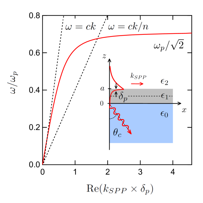
We consider here a simple tunnel junction made of two thick metallic layers with a total thickness separated by a thin layer of insulator. We can therefore distinguish two kinds of surface plasmon polariton (SPP) modes, the fast modes localized at the surfaces of the electrodes and the slow mode localized inside the tunneling barrier of thickness . However, only the fast mode at the vacuum interface is coupled to the propagating mode in the sapphire substrate (see inset in FIG. 10). In the following, we then model the junction by a single metallic film of thickness . In the preliminary approximation, we can consider the dispersion relation of a semi-infinite metallic layer Maier :
| (26) |
where is the Drude dielectric constant of the metal described by the plasma frequency and the damping term and is the dielectric constant of the vacuum. In aluminum, reference Ordal et al. (1985) gives , and . FIG. 10 shows the theoretical expectation of Eq. (26). In the low frequency limit , the fast SPP mode reduces to with and can leak in the substrate at the specific angle such that .
VI.1 Coupling in the Kretschmann configuration
We now consider a thin metallic layer of thickness deposited on a substrate characterized by a dielectric constant to evaluate the leakage radiation (see inset in FIG. 10). We can assume that the thickness of the tunneling barrier has no effect on the field in the metallic electrodes. The component of the electric field in the junction is expressed by:
| (27a) | ||||
| (27b) | ||||
| (27c) | ||||
with . At the lowest non-trivial order in :
| (28a) | ||||
| (28b) | ||||
| (28c) | ||||
By implementing the boundary conditions of continuity of the electric and magnetic field parallel to the surface, we get:
| (29) |
with . The dispersion relation is then solution of equation which gives at the first non-trivial order:
| (30) |
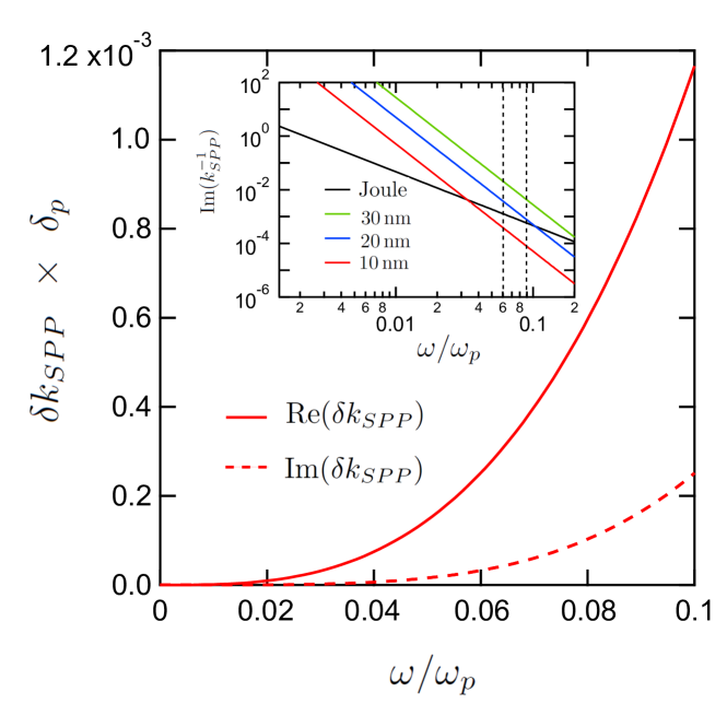
FIG. 11 shows as a function of frequency in the low frequency limit . Its inset compares the coupling length for different thickness to the Joule dissipation length:
| (31) |
It confirms that radiative damping is dominating for our experimental parameters and .
VI.2 Electric and magnetic fields in the tunnel junction
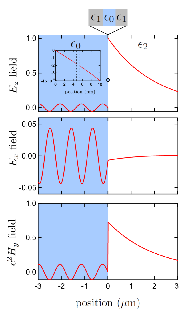
FIG 12 shows the profile of the electric and magnetic fields components at . and are continuous whereas exhibits discontinuities. The component of the electric field inside the tunnel barrier can be considered constant and is given at the third order in by:
| (32) |
where is also the dielectric constant of the alumina which is the same as sapphire. Note that the mode in the substrate is oscillating due to the radiative leakage of the SPP in the Kretschmann configuration.
VI.3 Radiation impedance in the low frequency limit
The Laks-Mills theory of light emission in a tunnel junction gives a radiated spectral power as a function of the two point spectral noise density and the component of the electric field inside the tunneling barrier Laks and Mills (1979, 1980); Ushioda et al. (1986):
| (33) |
where is the vacuum impedance. By assuming a position independent electric field () and a position independent tunneling current (), we get the radiation impedance:
| (34) |
In the low frequency limit , according to Eqs. (28a)(28b)(28c) and Eq. (29), the -dependence in only appears in whereas and . The integrand in Eq. (34) is thus dominated by its value in the region close to the pole:
| (35) | |||||
when follows the contour with (see inset of FIG. LABEL:figS9):. Substituting Eqs. (29) and (32) in Eq. (34), the lozentian approximation of the integrand leads to the radiation impedance in the low frequency limit :
| (36) |
Unlike the low frequency noise which is bonded by the frequency cut-off (), the spectral power density at optical frequencies involves the radiation impedance which does not exhibit any high-frequency cut-off. This radiation impedance corresponds to a directed emission at angle with:
| (37) |
Note that the angle of emission is slightly greater than the angle of total internal reflection of the flat substrate which explains the role of the conical prism. The radiation impedance due to the coupling between the tunneling current and the electromagnetic field is estimated at for . We can also estimate the radiation impedance due the coupling of the current in the electrodes but the screening factor of the electric field in the metal leads to which disagrees with experiment. Note that our calculation neglects the Drude dissipation compared to the plasmon leakage in the substrate.
VI.4 Photon emission efficiency in a metallic tunnel junction
The emission efficiency is usually defined by an electron to photon conversion rate:
| (38) |
However, as explained in the article, it is more relevant to define it with respect to the Joule power dissipated in the tunnel junction:
| (39) |
FIG. 14 shows the theoretical current noise spectral density for different bias voltage. The junction is characterized by the set of parameters defined in section III.1. It exhibits the cross-over at as expected. It enables to numerically calculate the efficiency and demonstrate the relationship between the efficiency and the ratio (see inset of FIG. 14):
| (40) |
where in the low frequency limit where the radiation impedance is given by Eq. (36). Note that is voltage dependent at low bias voltage giving rise to an increased efficiency. This is an artifact due to the black body radiation which are always emitting even at zero bias voltage. is a constant weakly dependent on the details of the barrier and depends mainly on the frequency dependence of the radiation impedance. Its numerical value is indeed close to find for a tunnel junction with constant transmission at zero temperature in the low frequency limit :
| (41) |
References
- Nyquist (1928) H. Nyquist, Phys. Rev. 32, 110 (1928).
- Callen and Welton (1951) H. B. Callen and T. A. Welton, Phys. Rev. 83, 34 (1951).
- Lambe and McCarthy (1976) J. Lambe and S. L. McCarthy, Phys. Rev. Lett. 37, 923 (1976).
- Kirtley et al. (1981) J. Kirtley, T. N. Theis, and J. C. Tsang, Phys. Rev. B 24, 5650 (1981).
- Hanisch and Otto (1994) M. Hanisch and A. Otto, Journal of Physics: Condensed Matter 6, 9659 (1994).
- Rogovin and Scalapino (1974) D. Rogovin and D. Scalapino, Annals of Physics 86, 1 (1974).
- Lee and Levitov (1996) H. Lee and L. S. Levitov, Phys. Rev. B 53, 7383 (1996).
- Sukhorukov et al. (2001) E. V. Sukhorukov, G. Burkard, and D. Loss, Phys. Rev. B 63, 125315 (2001).
- Roussel et al. (2016) B. Roussel, P. Degiovanni, and I. Safi, Phys. Rev. B 93, 045102 (2016).
- Basset et al. (2010) J. Basset, H. Bouchiat, and R. Deblock, Phys. Rev. Lett. 105, 166801 (2010).
- Gabelli and Reulet (2008) J. Gabelli and B. Reulet, Phys. Rev. Lett. 100, 026601 (2008).
- Parlavecchio et al. (2015) O. Parlavecchio, C. Altimiras, J.-R. Souquet, P. Simon, I. Safi, P. Joyez, D. Vion, P. Roche, D. Esteve, and F. Portier, Phys. Rev. Lett. 114, 126801 (2015).
- (13) For more information, see the Supplemental Material .
- Evans et al. (1993) D. J. Evans, E. G. D. Cohen, and G. P. Morriss, Phys. Rev. Lett. 71, 2401 (1993).
- Esposito et al. (2007) M. Esposito, U. Harbola, and S. Mukamel, Phys. Rev. B 75, 155316 (2007).
- Bardeen (1961) J. Bardeen, Phys. Rev. Lett. 6, 57 (1961).
- Büttiker and Landauer (1982) M. Büttiker and R. Landauer, Phys. Rev. Lett. 49, 1739 (1982).
- Christen and Büttiker (1996) T. Christen and M. Büttiker, EPL 35, 523 (1996).
- Blanter and Büttiker (2000) Y. Blanter and M. Büttiker, Phy. Rep. 336, 1 (2000).
- Simmons (1964) J. G. Simmons, J. Appl. Phys. 35, 2655 (1964).
- Lesovik and Loosen (1997) G. B. Lesovik and R. Loosen, Jetp Lett. 65, 295 (1997).
- Zamoum et al. (2016) R. Zamoum, M. Lavagna, and A. Crépieux, Phys. Rev. B 93, 235449 (2016).
- Lü et al. (2013) J.-T. Lü, R. B. Christensen, and M. Brandbyge, Phys. Rev. B 88, 045413 (2013).
- Kretschmann (1972) E. Kretschmann, Optics Communications 6, 185 (1972).
- Bonnet and Gabelli (2010) I. Bonnet and J. Gabelli, European Journal of Physics 31, 1463 (2010).
- Kirtley et al. (1983) J. R. Kirtley, T. N. Theis, J. C. Tsang, and D. J. DiMaria, Phys. Rev. B 27, 4601 (1983).
- Laks and Mills (1979) B. Laks and D. L. Mills, Phys. Rev. B 20, 4962 (1979).
- Ushioda et al. (1986) S. Ushioda, J. E. Rutledge, and R. M. Pierce, Phys. Rev. B 34, 6804 (1986).
- Persson and Baratoff (1992) B. N. J. Persson and A. Baratoff, Phys. Rev. Lett. 68, 3224 (1992).
- Berndt et al. (1991) R. Berndt, J. K. Gimzewski, and P. Johansson, Phys. Rev. Lett. 67, 3796 (1991).
- Parzefall et al. (2015) M. Parzefall, P. Bharadwaj, A. Jain, T. Taniguchi, K. Watanabe, and L. Novotny, Nature Nanotechnology 10, 1058 (2015).
- Xu et al. (2014) F. Xu, C. Holmqvist, and W. Belzig, Phys. Rev. Lett. 113, 066801 (2014).
- Altimiras et al. (2016) C. Altimiras, F. Portier, and P. Joyez, Phys. Rev. X 6, 031002 (2016).
- Patiño and Kelkar (2015) E. J. Patiño and N. G. Kelkar, Applied Physics Letters 107, 253502 (2015).
- Lin et al. (2008) Z. Lin, L. V. Zhigilei, and V. Celli, Phys. Rev. B 77, 075133 (2008).
- Hansen and Brandbyge (2004) K. Hansen and M. Brandbyge, Journal of Applied Physics 95, 3582 (2004).
- Brinkman et al. (1970) W. F. Brinkman, R. C. Dynes, and J. M. Rowell, Journal of Applied Physics 41, 1915 (1970).
- Zemanová Diešková et al. (2013) M. Zemanová Diešková, A. Ferretti, and P. Bokes, Phys. Rev. B 87, 195107 (2013).
- Thibault et al. (2015) K. Thibault, J. Gabelli, C. Lupien, and B. Reulet, Phys. Rev. Lett. 114, 236604 (2015).
- Kubo (1957) R. Kubo, Journal of the Physical Society of Japan 12, 570 (1957).
- Safi and Sukhorukov (2010) I. Safi and E. V. Sukhorukov, EPL (Europhysics Letters) 91, 67008 (2010).
- (42) U. Gavish, Y. Imry, and Y. Levinson, cond-mat/0211681 .
- (43) S. A. Maier, Plasmonics: Fundamentals and Applications (Springer Science & Business Media).
- Ordal et al. (1985) M. A. Ordal, R. J. Bell, R. W. Alexander, L. L. Long, and M. R. Querry, Appl. Opt. 24, 4493 (1985).
- Laks and Mills (1980) B. Laks and D. L. Mills, Phys. Rev. B 22, 5723 (1980).