Tunable spin-polarized edge transport in inverted quantum-well junctions
Abstract
Inverted HgTe/CdTe quantum wells have been used as a platform for the realization of 2D topological insulators, bulk insulator materials with spin-helical metallic edges states protected by time-reversal symmetry. This work investigates the spectrum and the charge transport in HgTe/CdTe quantum well junctions both in the topological regime and in the absence of time-reversal symmetry. We model the system using the BHZ effective Hamiltonian and compute the transport properties using recursive Green’s functions with a finite differences’ method. Specifically, we have studied the material’s spatially-resolved conductance in a set-up with a gated central region, forming monopolar (n-n′-n) and heteropolar (n-p-n, n-TI-n) double junctions, which have been recently realized in experiments. We find regimes in which the edge states carry spin-polarized currents in the central region even in the presence of a small magnetic field, which breaks TRS. More interestingly, the conductance displays spin-dependent, Fabry-Perót-like oscillations as a function of the central gate voltage producing tunable, fully spin-polarized currents through the device.
pacs:
73.63.Hs, 73.40.-c, 85.75.-dI Introduction
The role of topology in the properties of electronic systems has gained renewed attention over the last decade with the discovery of several materials that support topologically-protected surface and edge states, dubbed “topological insulators” (TIs). Hasan and Kane (2010); Qi and Zhang (2011); Ando (2013) Particular attention has been given to 2D topological insulators, where the quantum spin Hall (QSH) effect Kane and Mele (2005) allows for edge electron transport through spin-polarized helical edge states. The theoretical proposalBernevig et al. (2006) and later observationKonig et al. (2007) of the QSH effect in HgTe/CdTe quantum wells has triggered intense activity in the study of these systems.
The electronic current in 2D topological insulators is carried by edge states protected by time-reversal symmetry (TRS). In the absence of TRS, backscattering between the edge modes becomes allowed and the gaplessness of the edge states is no longer guaranteed. It has been arguedKonig et al. (2007) that even a small magnetic field is sufficient to open a gap in the edge states, thereby suppressing edge transport in 2D topological insulators. The argument supporting this view comes from the early experimentsKonig et al. (2007) on HgTe/CdTe quantum wells which show that the magnetoconductance shows a cusp-like feature at zero field, quickly decaying as the field increases. Such behavior, however, can only be accounted for when a rather strong disorder (of the order of the bulk gap) is considered Maciejko et al. (2010) in addition to TRS breaking.
In many situations, however, breaking TRS does not imply a suppression of edge transport channels in these systems. Several theoretical studies Schmidt et al. (2009); Tkachov and Hankiewicz (2010); Buttner et al. (2011); Chen et al. (2012); Scharf et al. (2012); Raichev (2012); Durnev and Tarasenko (2016) as well as experimental evidence Gusev et al. (2011, 2013a, 2013b) point to a scenario where edge transport in HgTe/CdTe quantum wells (QWs) is quite relevant up to magnetic fields of a few Tesla. For instance, theory predicts Tkachov and Hankiewicz (2010); Chen et al. (2012); Scharf et al. (2012) a transition from helical QSH to chiral QHE edge states at a critical field of a few Tesla.
A recent theoretical study on HgTe/CdTe QWs has shown that for small system sizes the edge states remain unaffected by a combination of moderate disorder and weak magnetic fields.Essert and Richter (2015) The transport properties change in long samples when considering charge puddles. Essert and Richter (2015) This kind of disorder and the corresponding local potential fluctuations have been extensively studied in graphene systems. Martin et al. (2008); Mucciolo and Lewenkopf (2010); Das Sarma et al. (2011) It has been found that charge puddles give rise to a disordered landscape of - junctions that are key to understand the low energy electronic transport in realistic graphene samples.Cheianov et al. (2007); Lima and Lewenkopf (2016); Fan et al. (2017)
Some recent theoretical Zhang et al. (2010) and experimentalGusev et al. (2013b); Piatrusha et al. (2017) works have probed the transport properties of heteropolar lateral junctions in HgTe/CdTe QWs in the inverted regime. Reference Gusev et al., 2013b in particular investigates electronic transport of double junction systems by applying a gate voltage in the central region of a HgTe quantum-well Hall bar. By varying , the system can be tuned from an n-n′-n type junction (Fermi energy lying in the electron-like states of the junction) to n-p-n (Fermi energy lying in the hole-like states of the junction). When is tuned close to the charge neutrality point, , the Fermi energy lies near the gap of the central region and the transport across the junction is expected to be dominated, in the absence of magnetic field, by QSH edge states (“n-TI-n”).
The results presented in Ref. Gusev et al., 2013b show that, in the presence of a strong perpendicular magnetic field ( T) the system enters the quantum Hall regime. The longitudinal conductance displays plateaus consistent with those expected for graphene junctions in the QHE regime:Abanin and Levitov (2007); Williams et al. (2007) in a monopolar n-n′-n junction () and in the bipolar n-p-n junction (). In the n-TI-n configuration (), a non-quantized conductance value was measured. More intriguingly, well-defined conductance plateaus have not been observed for weaker magnetic fields. Gusev et al. (2013b) This regime has no clear interpretation yet, calling for further theoretical investigation.
In this paper, we present a simplified model to describe the weak field limit (non-QHE regime) of HgTe/CdTe QW junctions. We compute the transport properties of pristine HgTe/CdTe QWs and homopolar and heteropolar double junctions by combining a discrete model Hamiltonian with the recursive Green’s functions method (RGF). Lewenkopf and Mucciolo (2013) For concreteness, we consider the Bernevig-Hughes-Zhang (BHZ) model Bernevig et al. (2006) in the presence of a perpendicular magnetic field. Scharf et al. (2012, 2015)
We calculate the space-resolved transmission across different types of junctions (n-n′-n, n-edge-n, n-p-n) as a function of a gate voltage applied at the system central region and of an external magnetic field. The latter is believed to destroy the topological protection, since it allows for backscattering in the spin-polarized edge states. Interestingly, our results show that, for fields up to a few Tesla, there is always a range of where edge transmission in the central region dominates the transport properties. We refer to this configuration as an “n-edge-n” junction.
We show that some of the transport features of the studied -TI (or -TI) junctions bear similarities with the case of graphene junctions where the transmission to a region where the transport is forbidden can be understood in terms of “snake-like” states at the interface.Carmier et al. (2010, 2011)
One of our main results is that, in an n-edge-n junction, the combined effect of quantum interference from reflection at the junction barriers and edge-state backscattering due to the breaking of TRS creates a spin-dependent Fabry-Pérot pattern in the transmission amplitudes. These gate-controlled oscillations are strong enough to provide fully spin-polarized currents across the junction.
The paper is organized as follows. In Sec. II we present the BHZ model used to describe the HgTe junctions and discuss the recursive Green’s functions approach employed to investigate the local currents in the system. Our numerical results are presented in Sec. III, where we study the effect of a perpendicular external magnetic field on the transport properties across the junction. Finally, we present our concluding remarks in Sec. IV.
II Model and Methods
We describe the physical properties of HgTe/CdTe QWs at low energies and zero magnetic field using the 4-band BHZ Hamiltonian Bernevig et al. (2006)
| (1) |
where , and are matrices spanning the basis , that can be expressed in terms of Pauli matrices , namely
| (6) | ||||
| (9) |
and is the identity. The numerical parameters depend on system properties such as the QW thickness.
We caution that the indices “” and “” indicate degenerate Kramers pairs related by TRS in the low-energy effective model obtained from the original 6-band model for HgTe near the ( point.Bernevig et al. (2006) In this sense, the latter are not “pure” spin 1/2 states since the -states carry contributions from p-type heavy-hole bands with spin . However, to a good approximation, these states represent spin 1/2 states related by TRS Buttner et al. (2011); Scharf et al. (2012) and we will treat them as such in the present work. In addition, we will neglect inversion-breaking terms Durnev and Tarasenko (2016) which give rise to coupling between the spin up and the spin down sectors.
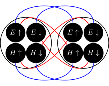
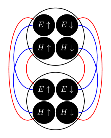
The numerical calculation of the QW transport properties follows the prescription of Ref. Scharf et al., 2012. We discretize the 4-component spinor in a square lattice of spacing in both and directions. The spinor becomes where and and and are integer. Figure 1 shows the orbital structure of the hopping matrix elements. We note that the hopping terms between electron and hole states are nonzero only if the spin projection is preserved.
Using two and three points derivatives for the momenta discretization
| (10) | ||||
the eigenvalue problem , becomes
| (11) |
where
| (12) | ||||
| (13) | ||||
| (14) | ||||
| (15) |
The above model Hamiltonian accounts for the presence of an external magnetic field perpendicular to the QW () by means of the gauge and by a Zeeman term Buttner et al. (2011) where contains the effective -factors for electrons and holes and is the Bohr magneton. The Peierls phase modifies the hopping matrix elements between the sites and in Eq. (13).
Comparisons with full 8-band calculations show that this low-energy model offers a good description for HgTe/CdTe QWs near the point for magnetic fields up to T.Schmidt et al. (2009)
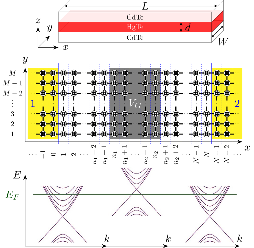
We address the transport properties of a QW of thickness , width , and length . The system is attached to left and right semi-infinite leads, aligned to its longitudinal direction, parallel to the -axis, as we illustrate in Fig. 2. For computational convenience the QW region is divided into transverse slices that are labeled by ranging from to , see Fig. 2. We model homopolar and heteropolar junctions by introducing a gate voltage acting on the system central region, corresponding to a term
| (16) |
for . In this way, we approximate the model Hamiltonian of Eq. (II) by a discrete Hamiltonian on a square lattice of dimensions , where and , containing orbitals in the central region.
The choice of the lattice parameter is a compromise between computational cost and accuracy. The value of is fixed as follows: We solve the eigenproblem in Eq. (11) using periodic boundary conditions in the direction for a chosen width in the direction. The reduced eigenvalue problem reads
| (17) |
where has the block structure and . Here is a matrix, given by Eqs. (12) to (15).
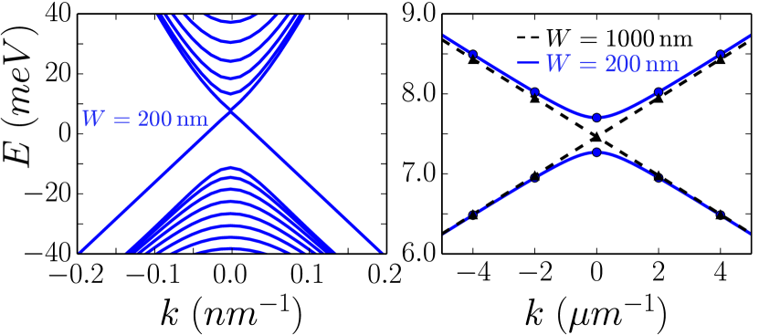
Due to translational invariance can be written as , where has components. For a given width we choose by requiring an accuracy of meV in the energy gap as compared to the analytical results obtained in Ref. Zhou et al., 2008. In practice, we fix for all calculations, which sets a lattice parameter for a given width . We find that this procedure satisfies the required accuracy for systems with m.
Figure 3 shows valence and conduction bands of two infinite HgTe/CdTe QWs of widths nm and nm obtained using the material parameters of a nm thick QW Zhou et al. (2008); Konig et al. (2008) , , , , in the absence of an external magnetic field (). We find that an HgTe/CdTe QW with nm presents a gap of about meV. The gap tends to close as we increase the width and reaches values as small as meV for nm.
We address the charge transport properties of the HgTe/CdTe QWs using the Landauer approach. Datta (1997); Haug and Jauho (2008) In the case of a vanishingly small source-drain bias, the zero temperature conductance of the system reads , where is the total transmission between the left and right contacts at the Fermi energy and
| (18) |
are the transmissions for each spin . Here () is the retarded (advanced) Green’s function for charge carriers with spin and () is the (spin-independent) line-width function accounting for the injection and life-time of the carriers states in the left (right) contact.
The discrete model Hamiltonian presented above allows for a very amenable implementation of the recursive Green’s functions technique.Lewenkopf and Mucciolo (2013) We compute the line-widths and with standard decimation methods Lopez Sancho et al. (1985) and the full retarded Green’s function in the system central region using the RGF. Lewenkopf and Mucciolo (2013) We gain additional insight by computing the local transmission
| (19) |
between two neighboring states and connected by the hopping matrix element for the charge current injected from the contact .
III Results
In this section, we analyze the magnetotransport properties of homopolar and heteropolar junctions in HgTe/CdTe QWs by studying the local transmission of different possible double junction system configurations, namely, n-n′-n, n-TI-n (n-edge-n for ), and n-p-n junctions. We present separately the analysis of the cases of (Sec. III.1) and (Sec. III.2).
III.1 Zero magnetic field
Here we study the charge transport through n-n′-n, n-TI-n, and n-p-n junctions in the presence of TRS, that is . As mentioned previously, we consider the case of an inverted HgTe/CdTe quantum well, in Eq. (II). Such systems support topologically-protected edge states when TRS is preserved. Thus, the “edge” portion of the junction represents a topological insulator.
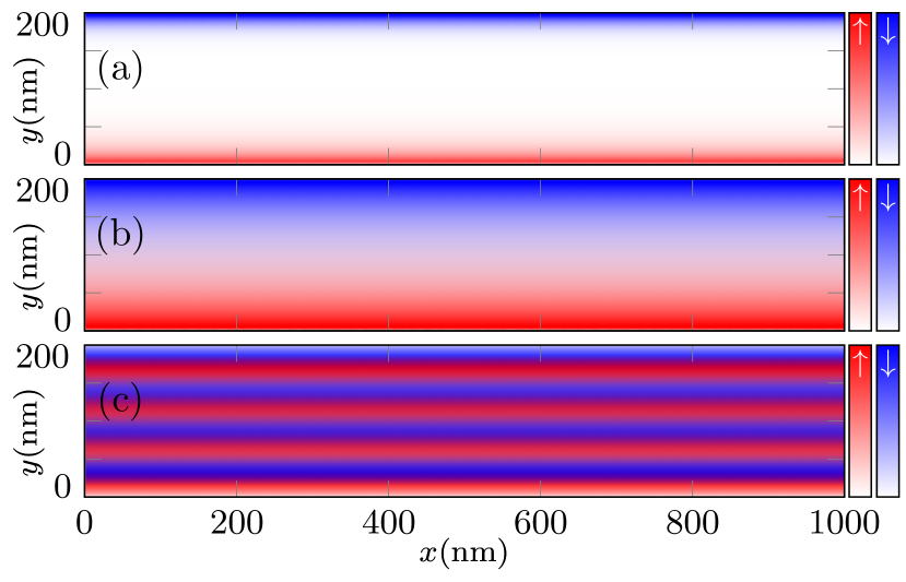
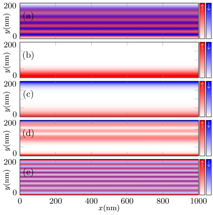
Let us begin discussing the case, where the system is uniform. Since here the spectrum is known (e.g., Fig. 3), the current profile serves to test the accuracy of our results and to introduce the tools we use in this study.
Using Eq. (19) we calculate the stationary local left-to-right transmission between the sites and as where () is the midpoint between the sites. For each value, we plot a color map of the normalized left-to-right transmission where is the maximum value of and is the fraction of composed by the spin component. In this scheme, the values of belong to the interval satisfying . Thus, for each varies between 0 and 1, with the unit representing full spin polarization and maximum transmission.
Typical results for are shown in Figure 4. For within the gap (Fig. 4a), there is only a single pair of states crossing the Fermi energy, which are localized at the QW edges. Thus, the current is carried by edge states with the expected spin texture of a topological insulator. As is tuned closer to the bottom of the conduction band, the local currents still flow mostly through spin-polarized states near the edges but the contribution from bulk states become more prominent, as shown in Fig. 4b.
In the n and p regions ( above and below the gap, respectively) there are well-defined spin-polarized stripes of current through the bulk. This is an interesting pattern: It implies a spatial separation of the spin-polarized currents through the bulk. This pattern originates from the different pairs of bulk and edge states crossing the Fermi level with positive group velocity, . The helical nature of the states implies that each pair will have opposite spins polarizations. Moreover, the states in each pair are mostly symmetrically localized around the center of the strip, in opposite sides of the system, creating the pattern shown in Fig. 4c.
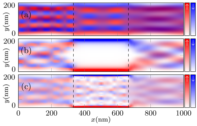
We now turn to the case. Depending on the magnitude of , we model a n-n′-n junction (Fig. 5a), a n-TI-n junction (Fig. 5b), or a n-p-n heteropolar junction (Fig. 5c). As we discuss below, these junctions are characterized by a very distinct current density flow behavior.
Now we fix at meV to study n-n′-n junctions (Fig. 5a). The current flow shows spin-polarized stripes across the QW transverse direction, similar to those observed for outside the gap in the case. The situation is different in the n-p-n configuration (Fig. 5c). Here, the stripe pattern in the central region seen in the n-n′-n junction vanishes due to the spatial mismatch between n-type and p-type states with positive group velocity. As a consequence of this mismatch, in the p-doped region the electronic transport is concentrated at the system edges, even though there are bulk states crossing the Fermi energy.
The n-TI-n configuration (Fig. 5b) shows a “spatial filtering”, where the current flows through spin-polarized edge states. Interestingly, reflections at the n-edge interface create a “snake-like” pattern for the spin-polarized currents.
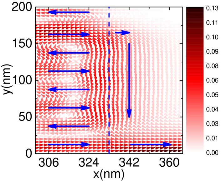
This is better illustrated by Fig. 6, where the spin up component of the transmission near the interface is shown for clarity. As previously discussed, in the TI region the spin up current is localized at the bottom edge. This behavior becomes increasingly clear as one moves away from the interface. Fig. 6 also shows a strong downward flow of spin up electrons parallel to the interface, represented by the (blue) vertical arrow. Spin up electron injected in the upper part of the junction cannot propagate the TI region and move along snake-like trajectories along the interface, Carmier et al. (2010, 2011) that channels the flow towards the system bottom edge.
On the n-doped side of the junction the behavior is strikingly different. The spin up electrons flow alternates in direction along the system transversal direction. As above, the bottom edge states also contributes to the left-right current in the n-region, producing a strong left-to-right spin up component matching the flux on the TI side. By contrast, the contribution from bulk states is either (i) reflected at the interface, producing small vortex-like patterns and a backward flow, or (ii) injected in the TI region in the upper section and then channelled downward along the interface. The combination of these two effects produces the current pattern in the n-doped region indicated by the (blue) horizontal arrows in Fig. 6.
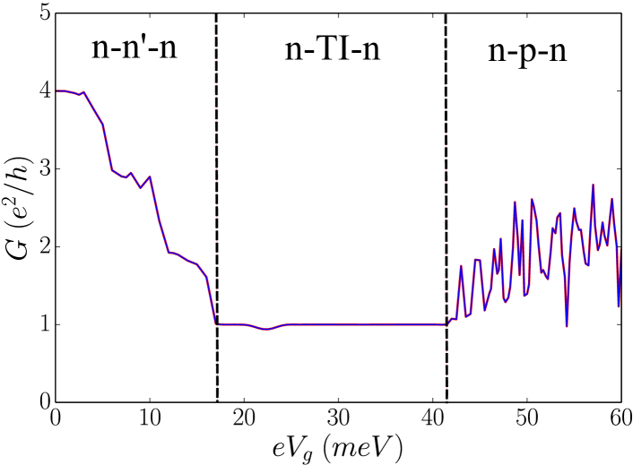
This picture allows us to interpret the conductance in these systems. Figure 7 shows the conductance per spin as a function of the gate voltage . The conductance plateaus in the n-n′-n region essentially count the number open modes at the Fermi energy in the central region for a given . As is tuned so that the lies inside the gap, a clear plateau appears. A small depression in the transmission near meV signals the presence of a finite-size gap in the spectrum. The gap is small enough so that the effective broadening arising from the coupling of the system to the contacts (which is captured by the RGF approach) is sufficient to give a large contribution to the transmission at that energy value. In the n-p-n region, the conductance oscillates rapidly with . This is a result of the multiple reflections and the wave mismatch between n and p regions. Note that the states with positive group velocity, that contribute to the left-to-right charge flow, have opposite phase velocity in n and p regions which enhance the mismatch between those states.
III.2 Transport at non-zero field
We now study the transport properties of HgTe QW junctions under an external perpendicular magnetic field . We consider QWs of nm. In this case, the transition to a regime where transport is dominated by quantum Hall-like chiral edge modes occurs at T.Scharf et al. (2012) Thus, we restrict our analysis to -fields up to T, where counter-propagating helical states are still present in the system.
As it is well known,Hasan and Kane (2010); Qi and Zhang (2011); Ando (2013) a magnetic field breaks TRS and thus the edge states lose their topological protection. Moreover, the Zeeman term in Eq. (II), although small, also breaks the spin degeneracy. The combination of these two effects substantially changes the spin-dependent transport properties across the junction.
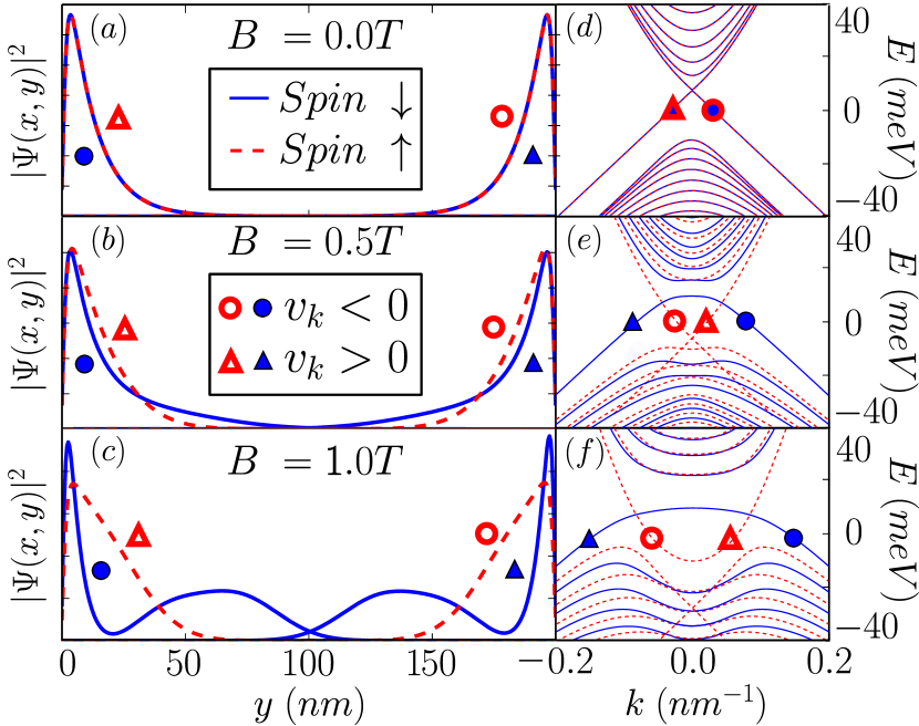
We begin by exploring the non-zero case for the case. Figure 8 contrasts the probability distributions of the system states at and the dispersion relations for representative values of . Consistent with previous studies, Chen et al. (2012) for T, a well-pronounced gap ( meV) appears for spin down states, while the spin up states show no-gap. As the field increases, the probability density of the spin up states remains concentrated at the edges, while the spin down states penetrate deeper into the bulk. This behavior is consistent with the local currents shown in Figs. 9b to 9d for selected values of the Fermi energy. In those cases, the asymmetry with respect to the axis (across the width) appears because only the forward moving states at one edge are present in the transport.
For n- and p-type transport Figs. 9a and 9e, respectively, the bulk currents flow along nearly spin-polarized stripes, similarly to the case. However, some interesting differences appear. When the Fermi energy lies inside the spin down gap, the current is fully spin-up polarized, flowing through the lower edge (Fig. 9b). As is tuned slightly below the spin up gap, the system shows spin-polarized transport on both edges, similar to the topological case, as shown in Fig. 9c. Note that the threshold for spin up bulk states is higher in energy than the spin down states, leading to a region where we have transport dominated by bulk spin up and edge spin down currents (Fig. 9d).
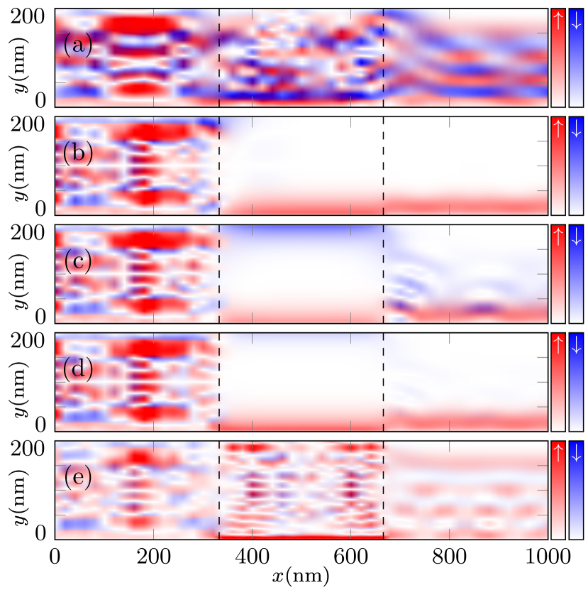
We now consider the local currents in HgTe n-(central)-n junctions at a finite magnetic field. Figure 10 shows the behavior for different values of such that lies close to the spin down local gap in the central region. Figures 10a and 10e correspond to n-n′-n and n-p-n junctions, respectively. In these cases the transport properties are dominated by bulk states and orbital interference effects.
When lies within the spin down gap, a spin up polarized current flows through the lower edge of the central region (Fig. 10b) and it is injected in the right n region through an edge state. A slight increase in (from 20 to 22.5 meV) is sufficient to bring to cross the first spin down edge state below the gap, thereby allowing spin down transport through the upper edge of the central region (Fig. 10c).
Surprisingly, a further small increase in (from 22.5 to 25 meV) causes the spin down current in the central region to practically vanish, as shown in Fig. 10d. This is at odds with the homogeneous case (Fig. 9) where spin down currents are always present as long as lies outside the spin down gap. We attribute this suppression to the large change in momentum across the n-edge junction necessary for the propagation of spin down electrons in the central region, as inferred from the band structure in Fig. 8e.
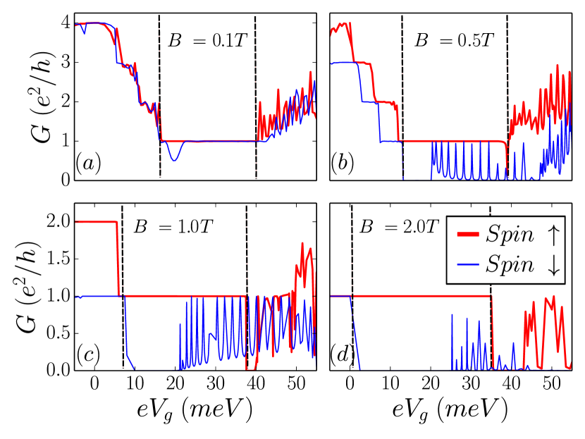
Let us now examine the conductance across the junction as a function of the gate voltage for T. Figure 11 shows a clear oscillatory pattern of the spin down current for meV up to the onset of n-p-n behavior at meV. In the same range, the spin up conductance remains at a plateau, indicating spin-polarized edge transmission for the values where the spin down current essentially vanishes.
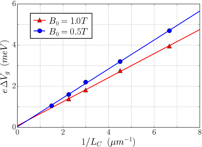
We associate these peaks with Fabry-Pérot resonances caused by backscattering at the junction interfaces. Figure 12 shows that the spacing between the transmission peaks displays a linear scaling with the inverse of the central region length , indicating single-particle interference due to backscattering at the interfaces. Similar phenomena has been investigated previously in two-terminal devices in the presence of a magnetic field. Tkachov and Hankiewicz (2010); Soori et al. (2012) Here, the presence of the interfaces magnifies the effect, leading to strong oscillations where a perfect spin-polarized transport across the junction is possible.
Fabry-Pérot-like oscillations also appear for larger magnetic field values and are suppressed for lower ones. In fact, the oscillations seem to occur only in the presence of a fully developed gap in the spin down spectrum, as shown in Figs. 11b and 11c.
For T, Fig. 11d, the behavior is similar. Since the spin down gap is significantly larger, the range of for which the current displays full spin up polarization increases from meV for T to meV for T. Interestingly, for larger values (meV), spin up drops to zero and full spin down polarization is now possible. Thus, for these moderate magnetic field values, the junction operates as a gate-tunable spin polarization switch.
IV Concluding remarks
In this paper we have theoretically studied the spin-dependent local currents in HgTe/CdTe quantum-well monopolar and heteropolar junctions. We considered the dependence of the transport properties with an applied magnetic field perpendicular to the sample and the resulting transition from topologically protected edge transport to a regime where spin backscattering is allowed at the junction barriers.
For zero magnetic field, our recursive Green’s functions calculations for the local currents show distinct characteristics for n-n′-n, n-TI-n and n-p-n junctions. While the bulk contributions to the current are strong in monopolar (n-n′-n) junctions, in the heteropolar case transport is dominated by edge states in the central region. In n-TI-n junctions, the spin-resolved flow alternates in direction along the system transverse direction in the n-side of the first n-TI interface. By contrast, the TI side shows currents flowing parallel to the interface toward the edges, where the main flow occurs.
Edge states still give a strong contribution to the transmission in the presence of TRS-breaking perpendicular magnetic field. Interestingly, the magnetic field opens a gap for one of the spins. Quantum interference due to backscattering at the interface produces spin-resolved Fabry-Pérot-like oscillations in the transmission as a function of the gate applied to the central region.
The combination of the gap opening and the Fabry-Pérot oscillations for only one of the spins allows for the production of tunable spin-polarized currents across the junction for moderate (T) values of the magnetic field. We stress that these results are generic for other inverted QWs displaying 2D topological insulator behavior such as InAs/GaSb.Du et al. (2015); Karalic et al. (2017) This opens the prospect for applications of inverted QW heteropolar junctions in spintronic devices.
Acknowledgements.
DN and LRFL acknowledge support from the Brazilian funding agencies CNPq, FAPERJ and Capes. LDS acknowledges support from CNPq grants 307107/2013-2 and 449148/2014-9, and FAPESP grant 2016/18495-4. CHL is supported by CNPq grant 308801/2015-6 and FAPERJ grant E-26/202.917/2015.References
- Hasan and Kane (2010) M. Z. Hasan and C. L. Kane, Rev. Mod. Phys. 82, 3045 (2010).
- Qi and Zhang (2011) X.-L. Qi and S.-C. Zhang, Rev. Mod. Phys. 83, 1057 (2011).
- Ando (2013) Y. Ando, J. Phys. Soc. Jpn. 82, 102001 (2013).
- Kane and Mele (2005) C. L. Kane and E. J. Mele, Phys. Rev. Lett. 95, 146802 (2005).
- Bernevig et al. (2006) B. A. Bernevig, T. L. Hughes, and S.-C. Zhang, Science 314, 1757 (2006).
- Konig et al. (2007) M. Konig, S. Wiedmann, C. Brune, A. Roth, H. Buhmann, L. W. Molenkamp, X.-L. Qi, and S.-C. Zhang, Science 318, 766 (2007).
- Maciejko et al. (2010) J. Maciejko, X.-L. Qi, and S.-C. Zhang, Phys. Rev. B 82, 155310 (2010).
- Schmidt et al. (2009) M. J. Schmidt, E. G. Novik, M. Kindermann, and B. Trauzettel, Phys. Rev. B 79, 241306 (2009).
- Tkachov and Hankiewicz (2010) G. Tkachov and E. M. Hankiewicz, Phys. Rev. Lett. 104, 166803 (2010).
- Buttner et al. (2011) B. Buttner, C. X. Liu, G. Tkachov, E. G. Novik, C. Brune, H. Buhmann, E. M. Hankiewicz, P. Recher, B. Trauzettel, S. C. Zhang, and L. W. Molenkamp, Nat. Phys. 7, 418 (2011).
- Chen et al. (2012) J.-c. Chen, J. Wang, and Q.-f. Sun, Phys. Rev. B 85, 125401 (2012).
- Scharf et al. (2012) B. Scharf, A. Matos-Abiague, and J. Fabian, Phys. Rev. B 86, 075418 (2012).
- Raichev (2012) O. E. Raichev, Phys. Rev. B 85, 045310 (2012).
- Durnev and Tarasenko (2016) M. V. Durnev and S. A. Tarasenko, Phys. Rev. B 93, 075434 (2016).
- Gusev et al. (2011) G. M. Gusev, Z. D. Kvon, O. A. Shegai, N. N. Mikhailov, S. A. Dvoretsky, and J. C. Portal, Phys. Rev. B 84, 121302 (2011).
- Gusev et al. (2013a) G. M. Gusev, E. B. Olshanetsky, Z. D. Kvon, N. N. Mikhailov, and S. A. Dvoretsky, Phys. Rev. B 87, 081311 (2013a).
- Gusev et al. (2013b) G. M. Gusev, A. D. Levin, Z. D. Kvon, N. N. Mikhailov, and S. A. Dvoretsky, Phys. Rev. Lett. 110, 076805 (2013b).
- Essert and Richter (2015) S. Essert and K. Richter, 2D Materials 2, 024005 (2015).
- Martin et al. (2008) J. Martin, N. Akerman, G. Ulbricht, T. Lohmann, J. H. Smet, K. v. Klitzing, and A. Yacoby, Nat. Phys. 4, 144 (2008).
- Mucciolo and Lewenkopf (2010) E. R. Mucciolo and C. H. Lewenkopf, J. Phys.: Condens. Matter 22, 273201 (2010).
- Das Sarma et al. (2011) S. Das Sarma, S. Adam, E. H. Hwang, and E. Rossi, Rev. Mod. Phys. 83, 407 (2011).
- Cheianov et al. (2007) V. V. Cheianov, V. I. Fal’ko, B. L. Altshuler, and I. L. Aleiner, Phys. Rev. Lett. 99, 176801 (2007).
- Lima and Lewenkopf (2016) L. R. F. Lima and C. H. Lewenkopf, Phys. Rev. B 93, 045404 (2016).
- Fan et al. (2017) Z. Fan, A. Uppstu, and A. Harju, 2D Materials 4, 025004 (2017).
- Zhang et al. (2010) L. B. Zhang, K. Chang, X. C. Xie, H. Buhmann, and L. W. Molenkamp, New Journal of Physics 12, 083058 (2010).
- Piatrusha et al. (2017) S. Piatrusha, V. Khrapai, Z. Kvon, N. Mikhailov, S. Dvoretsky, and E. Tikhonov, arXiv preprint arXiv:1703.09816 (2017).
- Abanin and Levitov (2007) D. A. Abanin and L. S. Levitov, Science 317, 641 (2007).
- Williams et al. (2007) J. R. Williams, L. DiCarlo, and C. M. Marcus, Science 317, 638 (2007).
- Lewenkopf and Mucciolo (2013) C. H. Lewenkopf and E. R. Mucciolo, J. Comp. Electron. 12, 203 (2013).
- Scharf et al. (2015) B. Scharf, A. Matos-Abiague, I. Žutić, and J. Fabian, Phys. Rev. B 91, 235433 (2015).
- Carmier et al. (2010) P. Carmier, C. Lewenkopf, and D. Ullmo, Phys. Rev. B 81, 241406 (2010).
- Carmier et al. (2011) P. Carmier, C. Lewenkopf, and D. Ullmo, Phys. Rev. B 84, 195428 (2011).
- Zhou et al. (2008) B. Zhou, H.-Z. Lu, R.-L. Chu, S.-Q. Shen, and Q. Niu, Phys. Rev. Lett. 101, 246807 (2008).
- Konig et al. (2008) M. Konig, H. Buhmann, L. W. Molenkamp, T. Hughes, C.-X. Liu, X.-L. Qi, and S.-C. Zhang, J. Phys. Soc. Jpn. 77, 031007 (2008).
- Datta (1997) S. Datta, Electronic Transport in Mesoscopic Systems (Cambridge University Press, 1997).
- Haug and Jauho (2008) H. Haug and A. J. Jauho, Quantum Kinetics in Transport and Optics of Semiconductors, Solid-State Sciences, Vol. 123 (Springer, Heidelberg, 2008).
- Lopez Sancho et al. (1985) M. P. Lopez Sancho, J. M. Lopez Sancho, and J. Rubio, J. Phys. F: Met. Phys. 15, 851 (1985).
- Soori et al. (2012) A. Soori, S. Das, and S. Rao, Phys. Rev. B 86, 125312 (2012).
- Du et al. (2015) L. Du, I. Knez, G. Sullivan, and R.-R. Du, Phys. Rev. Lett. 114, 096802 (2015).
- Karalic et al. (2017) M. Karalic, C. Mittag, T. Tschirky, W. Wegscheider, K. Ensslin, and T. Ihn, Phys. Rev. Lett. 118, 206801 (2017).