Hole spin resonance and spin-orbit coupling
in a silicon metal-oxide-semiconductor field-effect transistor
Abstract
We study hole spin resonance in a p-channel silicon metal-oxide-semiconductor field-effect transistor. In the sub-threshold region, the measured source-drain current reveals a double dot in the channel. The observed spin resonance spectra agree with a model of strongly coupled two-spin states in the presence of a spin-orbit-induced anti-crossing. Detailed spectroscopy at the anti-crossing shows a suppressed spin resonance signal due to spin-orbit-induced quantum state mixing. This suppression is also observed for multi-photon spin resonances. Our experimental observations agree with theoretical calculations.
pacs:
73.63.Kv, 73.23.Hk, 76.30.-vThe silicon-based metal-oxide-semiconductor field-effect transistor (MOSFET) is a key element of large-scale integrated circuits that are at the core of modern technology. Looking into the future, a universal fault-tolerant quantum computer also requires a huge number of physical qubits, on the order of or more QubitIntegration ; SC Review . As such, a qubit integrated with the standard Si MOSFET architecture would be truly attractive from the perspectives of scaling up and leveraging existing technologies. One example of such a qubit is the spin of an impulity/defect in the channel of a Si MOSFET. Indeed, spin qubits defined in Si nano-devices are not only compatible with current silicon technology, but are also known to be one of the most quantum coherent among known qubit designs JelezkoPRL2004 ; MorelloPRB2009 ; MorelloNature2010 ; KoehlNature2011 ; MortonReview2011 ; ZwanenburgReview2013 ; MuhonenNN2014 ; VeldhorstNN2014 ; pratiNN2012 ; buluta ; zalba16 .
Although there are many studies of impurities and defects in Si CompilationDefects , single impurity/defect in the channel of a Si MOSFET has only recently been studied experimentally, by single-electron tunneling Dot in MOS1 ; Dot in MOS2 ; Dot in MOS3 ; Dot in MOS4 ; Dot in MOS Ono . Spins of such defects are difficult to characterize because of their weakly-interacting nature. Controlling the spins of impurities in a MOSFET, as well as in a gate-confined quantum dot, can be achieved much more easily in a p-channel MOSFET than an n-channel. The reason is that the larger spin-orbit interaction (SOI) of a hole (-like) spin enables the spin resonance by an oscillatory electric field, instead of a magnetic field, at microwave frequencies under typical sub-Tesla static magnetic fields. Such electrically-driven spin resonance (EDSR) has been demonstrated in III-V devices GsAs EDSR ; III-V nanowire0 ; III-V nanowire ; III-V nanowire2 , as well as in Si CMOS Si ESR ; kawakami14 ; takeda16 , while SOI effects in gate-confined Si quantum dots have been investigated in the spin blockade region PMOS SB . However, systematic investigations of EDSR under the direct influence of SOI have not been performed in Si, the material that provides an ideal stage for studying SOI due to the minor presence of nuclear spins.
In this work we study sub-threshold transport and EDSR in a short p-channel Si MOSFET, and quantitatively reveal the effects of SOI and EDSR on lifting the spin blockade. Specifically, our transport measurements demonstrate that there are two effective dots in the channel, which allow us to identify a spin blockade regime and explore spin resonance for two strongly-coupled holes. The observed two-spin EDSR spectra, in particular the magnetic field dependence of the resonances, and the associated state mixing provide clear evidence of a SOI-induced anti-crossing with a well-resolved spin-orbit gap. Spectroscopy at the anti-crossing shows a suppressed EDSR signal because the involved states are almost equally populated as a result of the maximum SOI-induced state mixing. Our observations of spin blockade, single- as well as multi-photon spin resonance, and spin-orbit-induced state mixing are important steps toward the precise control of spin qubits in Si MOSFETs.
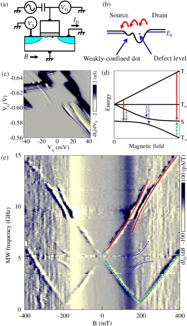
Our device is a p-channel MOSFET with a channel length of 135 nm and width of 220 nm, as shown in Fig. 1(a). It has a silicon oxynitride gate dielectric, and is fabricated with standard 0.13 m CMOS technology. The measurements are performed in a 4He pumped cryostat at a temperature of K. A magnetic field is applied parallel to the MOS interface and the source-drain current, and a microwave field is applied directly to the gate electrode. Figure 1(c) shows the measured current in the sub-threshold region. Specifically, we measure the source-drain differential conductance as we vary the source-drain () and gate () voltages. A Coulomb diamond with charging energy of 25 meV is observed centered around V. The current in this diamond is about three orders of magnitude smaller than the on-state current of the MOSFET, which is a clear evidence of Coulomb blockade. This has been observed in MOSFETs before and attributed to sequential tunneling through a single dopant/defect in the channel Dot in MOS1 ; Dot in MOS2 ; Dot in MOS3 ; Dot in MOS4 ; Dot in MOS Ono .
An important feature of Fig. 1(c), however, is that the Coulomb diamond around V does not close all the way to at both its ends near V and V (this is particularly clear near V). This indicates the presence of a larger dot that is detuned from and coupled in series with a more tightly confined dot, so that sequential tunneling through the double dot can only take place at finite source-drain bias. The data in Fig. 1(c) indicates that the two dots have a weak ( meV) and a strong ( meV) confinement. The strongly-confined dot could be a Boron dopant in the channel or a dangling bond defect at the silicon/oxynitride interface, whereas the weakly-confined dot could arise from potential fluctuations caused by remote impurities/defects. The physical system can then be represented schematically as shown in Fig. 1(b). Thermal cycles between 1.6 K and 300 K slightly shift the gate voltage dependence, but the Coulomb diamond and the microwave spectroscopy data remain the same after the cycles, indicating the robustness of the double dot.
An interesting regime of double quantum dots is the spin blockade regime, where spin symmetries are correlated with charge configurations SB . In our double dot device, we have evidence of spin blockade. Recall that in the spin blockade SB transport is blocked if the two-spin state is one of the triplet states, , , or . Lifting the spin blockade requires cotunneling and/or spin relaxation to the singlet state that consists of and components Petta_Science05 . Specifically, in the area enclosed by the dotted curve in Fig. 1(c), the current is suppressed outside the Coulomb blockade diamond, which indicates that details of the electronic states, such as spin symmetry, prevent electrons from sequential tunneling. Further evidence of spin blockade is revealed when the suppression of conduction is lifted by a microwave applied to the gate electrode, and well-defined current peaks appear depending on both the external magnetic field and the microwave frequency [Fig. 1(e)]. These microwave-induced peaks define the high-current curves seen in Fig. 1(e), and are due to spin excitations that lift the spin blockade which was originally in place. No EDSR was observed on the opposite side of the Coulomb diamond, for , mostly because the tunneling is asymmetric for a MOSFET that is forward- and reverse-biased.
The spectroscopic features of Fig. 1(e) can be qualitatively explained by the low-energy spectrum of two-hole spin states in a double dot [Fig. 1(d)], and also dove-tail nicely with the picture of current suppression due to spin blockade. In our double dot there is a singlet-triplet exchange splitting at zero magnetic field due to mixing between the and singlets Petta_Science05 . When a finite magnetic field is applied, the triplet states Zeeman-split, with one of the polarized triplets eventually crossing the singlet state. The SOI couples the triplet with the singlet and makes the crossing point into an anti-crossing. The magnitude of the anti-crossing gap is determined by the SOI matrix element between the and the , and in our device it is about 1 GHz. The two eigenstates near the anti-crossing are mostly mixtures of and singlets together with the triplet. The field at which the anti-crossing occurs, i.e., mT in Fig. 1(e), is determined by the zero-field exchange splitting and the -factors in the two dots.
The high-current curves in Fig. 1(e) can now be attributed to microwave-induced transitions between the mixed singlet-triplet states as indicated by the arrows in Fig. 1(d). Microwave-induced transitions among the triplet states ( to , i.e. the normal EDSR transitions) do not lift the spin blockade, thus cannot be observed in our transport experiment. SOI does not couple and states, thus we do not observe a horizontal current curve in Fig. 1(e), except near the anti-crossing, where the to transition is allowed and the spin blockade can be lifted because of the – mixing. Similar EDSR curves have also been observed in III-V nanowire double dots III-V nanowire . Notice that, in Fig. 1(e) the background current increases at mT, independent of the microwave frequency, giving a clear vertical contrast at these fields. This increase is consistent with the enhanced scattering rate due to the SOI-induced – mixing.
The EDSR spectra up to 40 GHz indicate that the -factor difference between the two dots is small compared with the zero-field singlet-triplet splitting of about 5 GHz Suppl . Assuming the same -factors, the slope of the current curves in Fig. 1(d) gives a -factor of 1.80. This is much larger than the value 1.1 observed for Boron dopants in bulk Si Boron g-factor , while smaller than the value 2.0 of the dangling bond defect centers at the silicon-oxynitride interface K center g-factor . We generally expect shallower defects to be more affected by the spin-orbit nature of the valence band, and their -factors should be smaller than the value of deep dangling bond defects. EDSR spectra as in Fig. 1(e) can be observed throughout the spin blockade area enclosed by the dotted curve in Fig. 1(c). The -factor does not change significantly in this area, while the exchange energy can change by a factor of 2 depending on . The typical linewidth of EDSR is 0.18 GHz, probably limited by the electrical charge noise due to the strong SOI in our device.We expect only a minor contribution of the nuclear spins to the EDSR linewidth due to the small content (4%) of 29-Si, and the p-orbital nature of holes.
It is emphasized that our experiment is performed at temperature of 1.6 K, which is over an order of magnitude higher than the usual temperatures of 0.1 K reported in previous works [20-26]. Performing the experiment at this high temperature is achieved thanks to the large orbital quantization energy of our dots. This gives also tolerance against unwanted photon-assisted tunneling or pumping current under strong driving.
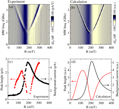
For a more precise understanding of our observations, we focus on the – transition near the anti-crossing point. This anti-crossing has never been observed before; neither in Si nor in III-V quantum dots. Figure 2(a) shows the leakage current () as a function of the microwave frequency and the magnetic field. The physics here can be well explained by a two-level model described in the Supplement Suppl . To summarize briefly, we incorporate the microwave driving by assuming that an electric field of amplitude and frequency modulates the on-site energy of dot 2 periodically, namely, . In other words, the transitions we study are purely electrically driven. The model considers the two energy levels and which anti-cross. The corresponding eigenstates are , , . The double dot parameters for are chosen so that the levels anti-cross at about mT, with a spin-orbit gap of about GHz. The coefficients , , , and are obtained by diagonalizing the double dot Hamiltonian in the absence of the microwave. When the microwave is turned on, we perform a unitary transformation into a rotating frame Suppl , and within a rotating wave approximation we obtain an approximate time-independent Hamiltonian for the single-photon spin resonance
| (1) |
with
| (2) |
where is the st order Bessel function of the first kind Suppl . We then calculate the current with a density matrix approach Suppl .
The theoretical results from this two-level model, shown in Fig. 2(b), are in good qualitatively agreement with the experimental observations in Fig. 2(a). There are two important features common to both figures, one being the broad peak in the background current () centered at about mT independent of the microwave frequency. This peak is the result of the SOI-induced singlet-triplet mixing. It has an asymmetric form Giavaras , unlike the usual symmetric lineshape in a two-level system. The other common feature of Figs. 2(a, b) is the high-current curve due to the microwave-induced – transition. The shape of this curve is hyperbolic, which arises from the normal anti-crossing of two straight lines. The two-level model we adopt here gives us a good qualitative description of the experimental observations. We do not attempt to achieve quantitative agreement because of the missing information with regard to the device, such as the exact interdot tunnel coupling and the microscopic spin-orbit coupling mechanism. For example, differences in the EDSR linewidths between experiment and theory are most probably due to different co-tunneling rates that limit the lifetime of spin states in the dots, as well as additional decoherence sources that are not accounted for in the model.
Experimental data in Fig. 2(c) demonstrate that near the anti-crossing at mT the background current reaches a maximum, while the EDSR-induced current has a minimum. This minimum occurs even though the transition rate between the two levels due to the microwave field is the highest because of the maximized singlet-triplet mixing. This interesting feature can be understood within the two-level model. Recall that the leakage current in the spin blockade is due to mixing of the triplet with the singlet state. The microwave field indeed tends to equalize the occupations of the two levels, but near the anti-crossing the SOI already generates the maximum possible singlet-triplet mixing, so that transport of the electrons occupying the triplet state is no longer blocked. This leads to a maximum in the leakage current, and transitions between the two states due to the microwave field cannot increase the current further. Thus the effect of the microwave is almost completely suppressed. This situation is similar to the well-known saturation of absorption under strong driving in spin resonance experiments ESR , where the microwave equalizes the populations of the two levels and eventually leads to a decrease in the resonance signal. Figure 2(d) shows the calculated single-photon EDSR-induced current peak height as well as the background current, which are in nice qualitative agreement with the experimental observations in Fig. 2(c). Notice that while at the – anti-crossing the microwave-induced – transition does not lead to further increase in current, the – and – transitions do lead to a current increase because they lift the spin blockade for electrons occupying the and states. In Fig. 1(c), the microwave-induced current increase is visible even at mT.
In Fig. 2 the EDSR-induced current peaks also diminish for [the feature is also apparent in Fig. 1(e)]. Within the two-level model, when the state becomes more exclusively the polarized triplet state, , so that the coupling term because . Thus, the microwave field becomes less efficient in inducing direct transitions from any of the triplet states to the singlet and the current peaks start to diminish for . A cautionary note here, however, is that the two-level model becomes increasingly inaccurate as , because in this limit the triplets become quasi degenerate. In the Supplement Suppl we discuss a more accurate calculation based on a Floquet master equation, which confirms the trends observed in Fig. 2.
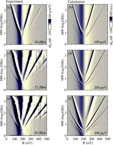
Multi-photon EDSR has been observed before in double dots at strong microwave driving 2 Photon coherent ESR ; Multi-photon ESR , away from the – anti-crossing. As shown in Figs. 3(a, c, e), when we increase the microwave power in our device we can generate additional current peaks. These peaks correspond to , 3, or more photons inducing transitions between the two levels that anti-cross. The resulting multi-photon high-current curves are extrapolated to the of the spin-orbit gap at mT. The multi-photon peaks can be reproduced with the two-level model discussed above when we use the appropriate -photon Hamiltonian Suppl . The theoretical results in Figs. 3(b, d, f) are in good qualitatively agreement with the experiment. Increasing the microwave amplitude gives rise to extra current peaks, in addition to the primary single-photon one, corresponding to the successive -photon resonance . Here results up to four-photon transitions are shown. As derived in the Supplement Suppl the Hamiltonian describing the -photon transition depends on . Therefore, in Figs. 3(b, d, f) we consider , and for each frequency we plot the corresponding maximum increase in the background current that comes from a specific . This way produces the correct behaviour near the -photon peak.
In summary, we studied a p-channel Si MOSFET and identified a spin blockade regime in a double dot system formed by a pair of defects/impurities in the channel. We experimentally observed electrically-driven two-spin resonance and found that the spin-orbit interaction suppresses the spin resonance signal near the anti-crossing point for both single- and multi-photon resonances. Our work shows that impurities/defects in commercial-quality Si MOSFET can be addressed straightforwardly, and they provide a useful window into the electronic spectrum and quantum coherent dynamics. This revelation is particularly appealing when we consider the great practical advantages that silicon industry could provide to fabricating quantum coherent devices.
We thank M. Kawamura, K. Ishibashi, K. Itoh, S. Kohler, and S. Shevchenko for discussions. This work was supported by JSPS KAKENHI Grant No. 15H04000. This work was partially supported by the RIKEN iTHES Project, the MURI Center for Dynamic Magneto-Optics via the AFOSR Award No. FA9550-14-1-0040, the Japan Society for the Promotion of Science (KAKENHI), the IMPACT program of JST, CREST, US ARO, and a grant from the John Templeton Foundation.
Appendix A Double quantum dot: Coulomb diamond and current
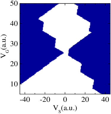
Most of the features of the open Coulomb diamond structure in Fig. 1(c) in the main article can be well reproduced by a simple calculation based on the constant charging-energy model. If (, ) is the number of holes on dot , then the energy of dot 1 is , and the energy of dot 2 is . Here, (, 2) and denote an on-site and an inter-dot charging energy respectively. Also, and are the lever arms of and , while is the energy offset between the dots. The Coulomb blockade is lifted for . Figure S1 shows the typical Coulomb diamond structure for a double quantum dot when one of the dots has large charging energy, and the other dot has small charging energy.
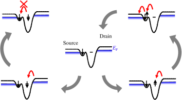
In Fig. 1(c) in the main article, a region where spin blockade occurs was identified. The transport cycle in the spin blockade regime is shown schematically in Fig. S2. As explained in the main article the spin-orbit interaction and the microwave field can lift the spin blockade by inducing singlet-triplet transitions.
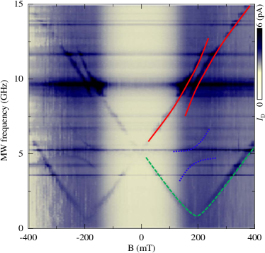
As a result a measurable leakage current flows through the double dot. Figure S3 shows the intensity plot of the leakage current for the same scale of magnetic field and MW frequency as that in Fig. 1(e) in the main article (where was presented). The high-current curves are due to microwave-induced transitions between the mixed singlet-triplet states. The series of resonances at constant frequency are due to photon-assisted tunneling enhanced by cavity modes.
Appendix B Spin resonance for large magnetic field
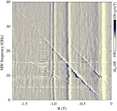
In the main article we presented EDSR spectra near the – anti-crossing point. Here we show additional spectra for a microwave frequency up to 40 GHz and magnetic field up to 1.7 T. In Fig. S4 three nearly-straight lines are visible. As explained in the main article, two of these lines map-out the transitions between the states and . The lower line corresponds to the 2-photon – transition. For a double quantum dot with large difference in the -factors, the lines – are not parallel at high magnetic fields. Investigation of the data shown in Fig. S4 demonstrates that in our system these lines are parallel within at least 2% accuracy, indicating that the -factor difference in the two dots is small enough compared with the zero-field singlet-triplet splitting of about 5 GHz.
Appendix C On the microwave attenuation and nonlinearity
In this section we present some details about the microwave field.
If we assume a 50 Ohm impedance for our transmission line, then
the MW power (in dBm) used in the experiment [Fig. 2(a) and
Fig. 3(a,
c, e)], and the corresponding MW amplitude (in mV) are:
-40 dBm 2.2 mV,
-30 dBm 7.1 mV,
-22 dBm 17.8 mV,
-20 dBm 22.4 mV.
For the calculations [Fig. 2(b) and Fig. 3(b, d, f)] we have the
following correspondence:
-87 dBm 0.01 mV,
-67 dBm 0.1 mV,
-61 dBm 0.2 mV,
-55 dBm 0.4 mV.
The experimental and theoretical numbers are quite different, suggesting a very large attenuation and nonlinearity. An estimated attenuation of our rigid coaxial cable with a 2 m length is only 3 dB at 5 GHz. This very large attenuation and nonlinearity may be due to the bare wiring of about 1 cm length between the end of the coax and our device, as well as the nonlinearity of the capacitance. Our MOSFET device is set around the subthreshold regime, thus the capacitance will be affected by the voltages , as well as the MW power, if a strong power starts to cause photon-assisted tunneling or charge pumping current.
Appendix D System Hamiltonian
In this section we describe the Hamiltonian of the physical system. We consider a double quantum dot (DQD) coupled to metallic leads. The total Hamiltonian of the system is
| (3) |
where is the DQD Hamiltonian, is the Hamiltonian of the leads, and is the interaction Hamiltonian between the DQD and the leads. Specifically, the DQD Hamiltonian is
| (4) | |||||
where is the number operator , and the operator () creates (destroys) a hole on dot , 2, with spin and orbital energy . We assume a single-band description and consider the holes to have spin 1/2. In this case the two-hole Hilbert space is spanned by the singlet and triplet states , , , , , where is a singlet state with () holes on dot 1 (dot 2).
The orbital energies of the two dots are
| (5) |
where denotes the energy detuning. The external electric field has amplitude and cyclic frequency , and when the DQD Hamiltonian is time dependent . This configuration of the orbital energies results in a localised spin in dot 2 during the transport cycle in the spin blockade regime.
Each dot has a charging energy , and -factor which leads to a Zeeman splitting due to the external magnetic field . The inter-dot tunnel coupling with strength is modelled by the Hamiltonian
| (6) |
and the non spin-conserving inter-dot tunnel coupling due to the spin-orbit interaction (SOI) is modelled by the Hamiltonian stehlik ; Giavaras
| (7) |
This simplified Hamiltonian couples () to states, thus for example the lowest singlet-triplet levels anti-cross and the induced gap is proportional to the SOI tunnel coupling . For a fixed the anti-crossing gap is sensitive to the detuning because this controls the amplitude of the component in the quantum states. A rigorous derivation of a microscopic SOI Hamiltonian golovach should consider the detailed geometry of the quantum dot system which in the present device is unknown. Nevertheless, Eq. (7) allows us to reproduce the basic experimental features.
The DQD is tunnel-coupled to left and right leads, which consist of non-interacting holes. These holes are described by the Hamiltonian
| (8) |
where the operator () creates (destroys) a hole in lead with momentum , spin , and energy . The interaction Hamiltonian between the DQD and the two leads is
| (9) |
with being the tunnel coupling between dot 1 (2) and the left (right) lead, which is assumed to be energy independent, and we also consider .
Appendix E Two-level model
E.1 Two-level Hamiltonian
In the main article an effective two-level Hamiltonian was used to explore the microwave-induced peaks. Here we give some details about the derivation of this Hamiltonian. First we diagonalize the time-independent part of the DQD Hamiltonian . The derived eigenenergies are denoted by and the corresponding eigenstates are written in the general form
| (10) |
For only one state the coefficient and specifically , and for simplicity we neglect the component , but this is taken into account in the numerical computations. Then we write the total DQD Hamiltonian in the energy basis . To look for an analytical treatment, we assume that the two eigenstates , , which form the anti-crossing point, can approximate well the dynamics of the system and thus we ignore all the other eigenstates. These arguments lead to the following approximate DQD Hamiltonian
| (11) |
where , are the two energy levels which anti-cross. Then to remove the time dependence from the diagonal elements of , we perform a transformation to derive the transformed Hamiltonian grifoni
| (12) |
with the operator
| (13) |
and the phases
| (14) |
The transformed Hamiltonian is
| (15) |
with the off-diagonal coupling element being
| (16) | |||||
and the parameter . To simplify this expression we use the formula
| (17) |
where is the th order Bessel function of the first kind. Then the coupling term is
| (18) | |||||
In the context of a ‘rotating wave approximation’, we assume that in the long-time limit, when the system has reached the steady state, the non-oscillatory terms can approximate well the dynamics. Thus, the off-diagonal element becomes time-independent
| (19) |
Using the property and substituting , we arrive at the off-diagonal coupling element
| (20) |
We use the effective DQD Hamiltonian to study the -photon resonance that satisfies the condition . For , the Hamiltonian coincides with the Hamiltonian in Eq. (1) given in the main article. When there is no driving, , the coupling is ; thus the two levels are uncoupled and there are no microwave-induced peaks. Moreover, when one of the coefficients is zero; thus and the driving field cannot couple the two levels. Finally, the parameters in this work satisfy the regime with , consequently at a given magnetic field the single-photon peak is stronger than the -photon peak. This observation is consistent with the experimental data.
E.2 Rate equations
In the spin blockade regime the electrical transport takes place through the charge-cycle , where (, ) refers to a state with () holes on dot 1 (dot 2). We consider the single-spin states , , as well as the two-hole states that form the anti-crossing , , and determine the density matrix of the DQD in the transformed frame (‘rotating’ frame). Following a standard open-system approach blum the equation of motion of can be written in the form
| (21) |
where the incoherent term accounts for the interaction of the DQD with the two leads which is treated to second order in the dot-lead tunnel coupling (sequential tunneling). In this approximation the transition rates between the DQD eigenstates due to the coupling of the DQD with the leads acquire a simple form Giavaras . The effect of the transformation on the DQD-lead interaction is ignored and Eq. (21) can be solved analytically in the steady state, e.g., when . In this effective model the electrical current through the DQD is proportional to the population of the state, which is extracted directly from the populations of and .
Appendix F Floquet model
The effective two-level model described in the preceding section takes into account only the states which form the anti-crossing point and neglects the time-dependent oscillating terms in the Hamiltonian. In the spin blockade charge-cycle all triplet states are relevant Giavaras , and in the limit the triplet states become quasi degenerate, thus the effective model is questionable. Therefore, to test the overall accuracy of the effective model, we describe in this section another model that takes into account all the states which are involved in the transport through the DQD note1 , and treats the time dependence of the DQD Hamiltonian exactly within the Floquet formalism platero ; chu ; kohler .
F.1 Floquet Hamiltonian
The Hamiltonian of the DQD is periodic , with being the period of the external electric field. For this reason it is convenient to apply the Floquet formalism which is a powerful tool for time-dependent periodic systems platero ; chu ; kohler . According to the Floquet theorem, a solution of the time-dependent Schrödinger equation with a periodic Hamiltonian can be written in the form
| (22) |
where are the Floquet modes which have the periodicity of the Hamiltonian, i.e., , and are the Floquet energies. These are time independent and can be defined, for instance, within the interval . The Floquet modes and energies satisfy the following eigenvalue problem brune
| (23) |
that is solved by expanding the time periodic and in a Fourier series:
| (24) | |||||
| (25) |
If we denote by the basis vectors spanning the DQD Hilbert space, and expand in that basis
| (26) |
the eigenvalue problem Eq. (23) becomes
| (27) |
Here the indexes , refer to the Fourier series, and the indexes , refer to the basis vectors. For the numerical computations, this infinite system of coupled equations is truncated to a finite but sufficiently large value to ensure good convergence of the results.
F.2 Master equation
In the Floquet formalism, the density matrix of the DQD is expressed in the time-dependent Floquet basis , simplifying drastically the calculation of the steady state platero ; chu ; kohler . Within the Born and Markov approximations, the matrix elements satisfy the master equation
| (28) |
with , and the transition rates and quantify the interaction of the DQD with the two leads. For simplicity, here we focus only on and consider only the interaction of dot 1 with the left lead. The coupling of the DQD to the right lead can be treated in a similar manner. The rate is defined by the Fourier expansion
| (29) |
| (30) |
where is the Fermi distribution at the chemical potential of the left lead and . The subband index is defined by the index . The DQD-lead coupling constant is proportional to , and the matrix element is defined through its Fourier transform as follows
| (31) |
For any two system operators and , with , the corresponding matrix elements satisfy . To solve Eq. (28) we assume that in the long-time limit the density matrix, which describes the steady state, has the same periodicity as the DQD Hamiltonian, thus it can be expressed in the form
| (32) |
Substituting Eq. (29) and Eq. (32) into Eq. (28) results in an infinite set of coupled equations that is solved numerically by truncating to a finite value. Having determined the steady state, the tunneling current is computed by taking the average of the current operator , where is the number of holes in the right lead.
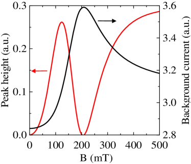
Figure 2 shows the background current and the microwave-induced peak height near the – anti-crossing point for a microwave amplitude eV. The basic features are in good overall agreement with the experimental data [see main article Fig. 2(c) and (d)]. The height of the current peaks is sensitive to the DQD-lead coupling and the microwave amplitude . When is strong, has to be large for the peaks to be visible. However, the computational time increases quickly with , because the Fourier expansions need extra terms to converge. For this reason, to keep the numerical problem tractable we choose in the GHz range.
A more detailed fit to the background current can be achieved by coupling the DQD to a bosonic bath and introducing spin flips chorley11 ; giavaras20 . This approach offers limited additional insight into the present experimental data, whilst extra parameters have to be introduced to specify the spectral density of the bath. Therefore, this approach is not pursued in this work. Three-body states which for simplicity are not accounted for in our model can also have some contribution to the background current giavaras20 .
Finally, we mention that the Floquet model can also be used to assess the rotating wave approximation [Eqs. (18), (19)] in the effective two-level model. In this case the Hamiltonian in Eq. (23) has to be replaced by [Eq. (11)]. The two models are in agreement.
Appendix G Double quantum dot parameters
The experimental data suggests that the charging energies of the two dots are meV and meV and the -factor is (see main article). In the calculations we take for the two dots , though this assumption is not important. In the experiment an anti-crossing point is probed at about mT and the anti-crossing gap is about 1 GHz, but the exact values of the parameters , , and are unknown. Consequently, for the calculations we choose , , and in order to form an anti-crossing point as in the experiment, and simultaneously to achieve a good qualitative agreement between the calculated and the measured background currents (). The SOI Hamiltonian forms two anti-crossing points, but the observed spectra indicate that only one point is relevant for the chosen ranges of the magnetic field and the driving frequency. The choice of the parameters , , and is not unique and we choose different values in the two models in order to achieve a good fit to the background current. In the two-level model, the parameters are meV, meV, and ; and in the Floquet model the parameters are meV, meV, and . Here, we present results for , but the models can also produce the general experimental features for .
References
- (1) N. C. Jones, R. Van Meter, A. G. Fowler, P. L. McMahon, J. Kim, T. D. Ladd, and Y. Yamamoto, Phys. Rev. X 2, 031007 (2012).
- (2) A. G. Fowler, M. Mariantoni, J. M. Martinis, and A. N. Cleland, Phys. Rev. A 86, 032324 (2012).
- (3) F. Jelezko, T. Gaebel, I. Popa, A. Gruber, and J. Wrachtrup, Phys. Rev. Lett. 92, 076401 (2004).
- (4) A. Morello et al., Phys. Rev. B 80, 081307 (2009).
- (5) A. Morello, Nature 467, 687 (2010).
- (6) W.F. Koehl, B. B. Buckley, F. J. Heremans, G. Calusine, and D. D. Awschalom, Nature 479, 84 (2011).
- (7) J. J. L. Morton, D. R. McCamey, M. A. Eriksson, and S. A. Lyon, Nature 479, 345 (2011).
- (8) F. A. Zwandenburg et al., Rev. Mod. Phys. 85, 961 (2013).
- (9) J. T. Muhonen et al., Nature Nanotech. 9, 986 (2014).
- (10) M. Veldhorst et al., Nature Nanotech. 9, 981 (2014).
- (11) E. Prati, M. Hori, F. Guagliardo, G. Ferrari, and T. Shinada, Nature Nanotech. 7, 443 (2012).
- (12) I. Buluta, S. Ashhab, and F. Nori, Rep. Prog. Phys. 74, 104401 (2011).
- (13) M.F. Gonzalez-Zalba et al., Nano Lett. 16, 1614 (2016).
- (14) C. A. J. Ammerlaan et al., Schulz, Max (Ed.), Impurities and Defects in Group IV Elements and III-V Compounds, Landolt-Börnstein, New Series III/22b, Springer (1989).
- (15) G. P. Lansbergen et al., Nat. Phys. 4, 656 (2008).
- (16) K. Y. Tan et al., Nano Lett. 10, 11 (2010).
- (17) M. Pierre et al., Nat. Nanotech. 5, 133 (2010).
- (18) M. F. Gonzalez-Zalba et al., Nano Lett. 14 5672 (2014).
- (19) K. Ono, T. Tanamoto, and T. Ohguro, Appl. Phys. Lett. 103, 183107 (2013).
- (20) K. C. Nowack, F. H. L. Koppens, Y. V. Nazarov, and L. M. K. Vandersypen, Science 318, 1430 (2007).
- (21) S. Nadj-Perge, S. M. Frolov, E. P. A. M. Bakkers, and L. P. Kouwenhoven, Nature. 468, 1084 (2010).
- (22) S. Nadj-Perge, V. S. Pribiag, J. W. G. van den Berg, K. Zuo, S. R. Plissard, E. P. A. M. Bakkers, S. M. Frolov, and L. P. Kouwenhoven, Phys. Rev. Lett. 108, 166801 (2012).
- (23) J. W. G. van den Berg, S. Nadj-Perge, V. S. Pribiag, S. R. Plissard, E. P. A. M. Bakkers, S. M. Frolov, and L. P. Kouwenhoven, Phys. Rev. Lett. 110, 066806 (2013).
- (24) R. Maurand, X. Jehl, D. Kotekar-Patil, A. Corna, H. Bohuslavskyi, R. Laviéville, L. Hutin, S. Barraud, M. Vinet, M. Sanquer, and S. De Franceschi, Nat. Com. 7, 13575 (2016).
- (25) E. Kawakami et al., Nat. Nanotech. 9, 666 (2014).
- (26) K. Takeda et al., Sci. Adv. 2, 1600694 (2016).
- (27) H. Bohuslavskyi et al., Appl. Phys. Lett. 109, 193101 (2016).
- (28) K. Ono, D. G. Austing, Y. Tokura, and S. Tarucha, Science 297, 1313 (2002).
- (29) J. R. Petta, A. C. Johnson, J. M. Taylor, E. A. Laird, A. Yacoby, M. D. Lukin, C. M. Marcus, M. P. Hanson, and A. C. Gossard, Science 309, 2180 (2005).
- (30) H. Tezuka, A. R. Stegner, A. M. Tyryshkin, S. Shankar, M. L. W. Thewalt, S. A. Lyon, K. M. Itoh, and M. S. Brandt, Phys. Rev. B 81, 161203(R) (2010).
- (31) J. P. Campbell, P. M. Lenahan, A. T. Krishnan, and S. Krishnan, J. Appl. Phys. 103, 044505 (2008).
- (32) See supplemental material.
- (33) G. Giavaras, N. Lambert, and F. Nori, Phys. Rev. B 87, 115416 (2013).
- (34) C. P. Slichter, Principles of Magnetic Resonance, Springer (1990).
- (35) J. Stehlik, M. D. Schroer, M. Z. Maialle, M. H. Degani, and J. R. Petta, Phys. Rev. Lett. 112, 227601 (2014).
- (36) P. Scarlino, E. Kawakami, D. R. Ward, D. E. Savage, M. G. Lagally, M. Friesen, S. N. Coppersmith, M. A. Eriksson, and L. M. K. Vandersypen, Phys. Rev. Lett. 115, 106802 (2015).
- (37) J. Stehlik, M. Z. Maialle, M. H. Degani, and J. R. Petta, Phys. Rev. B 94, 075307 (2016).
- (38) V. N. Golovach, A. Khaetskii, and D. Loss, Phys. Rev. B 77, 045328 (2008).
- (39) M. Grifoni and P. Hänggi, Phys. Rep. 304, 229 (1998).
- (40) K. Blum, Density Matrix Theory and Applications (Springer, Berlin, 2012).
- (41) We neglect three-body states and consider in total 11 many-body states.
- (42) G. Platero and R. Aguado, Phys. Rep. 395, 1 (2004).
- (43) S. I. Chu and D. A. Telnov, Phys. Rep. 390, 1 (2004).
- (44) S. Kohler, J. Lehmann, and P. Hanggi, Phys. Rep. 406, 379 (2005).
- (45) P. Brune, C. Bruder, and H. Schoeller, Phys. Rev. B 56, 4730 (1997).
- (46) S. Chorley, , Phys. Rev. Lett. 106, 206801 (2011).
- (47) G. Giavaras, unpublished