Coupling ultracold atoms to a superconducting coplanar waveguide resonator
Abstract
We demonstrate coupling of magnetically trapped ultracold 87Rb ground state atoms to a coherently driven superconducting coplanar resonator on an integrated atom chip. We measure the microwave field strength in the cavity through observation of the AC shift of the hyperfine transition frequency when the cavity is driven off-resonance from the atomic transition. The measured shifts are used to reconstruct the field in the resonator, in close agreement with transmission measurements of the cavity, giving proof of the coupling between atoms and resonator. When driving the cavity in resonance with the atoms, we observe Rabi oscillations between atomic hyperfine states, demonstrating coherent control of the atomic states through the cavity field. The observation of two-photon Rabi oscillations using an additional external radio frequency enables the preparation of magnetically trapped coherent superposition states near the superconducting cavity, which are required for the implementation of an atomic quantum memory.
Introduction
Hybrid quantum systems of superconductors and atomic spin ensembles have been proposed Xiang et al. (2013); André et al. (2006); Henschel et al. (2010) for quantum information processing to overcome the limited coherence of superconducting qubits Kim et al. (2011); Paik et al. (2011). In the envisioned hybrid system, information is processed by fast superconducting circuits and stored in a cloud of cold atoms, which serves as a quantum memory Verdú et al. (2009); Patton and Fischer (2013a, b). Information is transferred between the two quantum systems using a superconducting coplanar waveguide resonator as a quantum bus. In recent years, coupling between superconducting structures and spin-systems such as nitrogen vacancy centres Kubo et al. (2010, 2011); Amsüss et al. (2011); Putz et al. (2014); Grezes et al. (2016) and ions in solid state systems Schuster et al. (2010); Probst et al. (2013) has been observed. Cold atoms coupled to superconducting resonators would furthermore enable the implementation of novel quantum gates Petrosyan et al. (2009); Petrosyan and Fleischhauer (2008); Pritchard et al. (2014); Sárkány, Fortágh, and Petrosyan (2015), the realization of a microwave-to-optical transducerHafezi et al. (2012) and on-chip micromasers Yu et al. (2017). The interaction between Rydberg atoms and three-dimensional superconducting microwave resonators has been a rich research topic, especially with regard to atom-photon interactions on the fundamental level Haroche and Raimond (2006). Research on planar superconducting structures, however, holds the promise of switchable interactions between the subsystems, integration with scalable solid-state circuitry Wallraff et al. (2004); DiCarlo et al. (2010); Lucero et al. (2012) and long information storage in the atomic ensemble. While long coherence times in cold atoms have been studied extensively Treutlein et al. (2004); Deutsch et al. (2010); Kleine Büning et al. (2011); Dudin, Li, and Kuzmich (2013); Bernon et al. (2013) and trapping and manipulation of atoms in the vicinity of superconducting chips has been demonstrated in a series of experiments Nirrengarten et al. (2006); Mukai et al. (2007); Roux et al. (2008); Minniberger et al. (2014); Müller et al. (2010); Weiss et al. (2015), coupling between trapped atoms and planar superconducting resonators has not been shown yet.
In this article, we demonstrate magnetic coupling of ultracold magnetically trapped atoms to a superconducting coplanar waveguide resonator operated at temperatures around 6 K. The cavity is near-resonant with the atomic hyperfine splitting of 87Rb and coherently driven by an external microwave synthesizer. We investigate both the dispersive as well as the resonant coupling regime. By driving the cavity off-resonantly with respect to the atoms, the atomic states reveal an AC-Zeeman shift under the influence of the microwave (MW) field Sárkány et al. (2014). This leads to a shift of the atomic transition frequency, which is measured by Ramsey interferometry. We use the AC-Zeeman shift to reconstruct the microwave intensity in the coplanar resonator. In contrast, when the cavity is driven at a frequency corresponding to an atomic transition, Rabi oscillations between atomic hyperfine states are observed.
Our measurements present a vital step towards the realization of a atom-superconductor hybrid system, paving the way towards the implementation of an atomic quantum memory coupled to a superconducting quantum circuit and the realization of microwave-to-optical transducers.
Results
Atomic ensembles trapped in a coplanar waveguide resonator
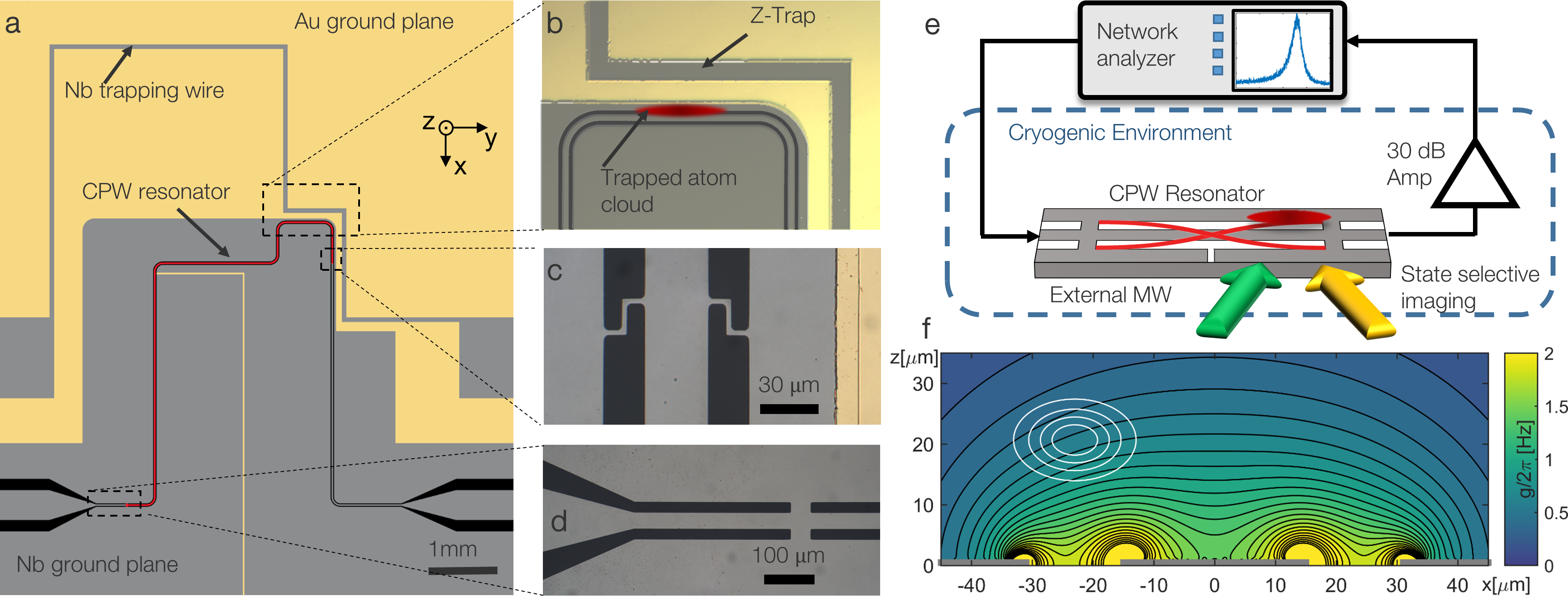
For our experiments, we magnetically trap an ensemble of ultracold 87Rb atoms in the state 5S close to a coplanar microwave resonator on an integrated atom chip. The chip comprises two essential structures: a Z-shaped wire for magnetic trapping of neutral atoms and a superconducting coplanar waveguide (CPW) resonator (Fig. 1).
The CPW resonator is an inductively coupled half wavelength cavity Bothner et al. (2017) with a fundamental mode resonance frequency GHz and a linewidth of MHz in the temperature range (K) relevant for the experiments described here. By varying the temperature of the atom chip, the resonance frequency of the microwave cavity can be tuned by about MHz, where the atomic hyperfine transition frequency GHz lies within this tuning range. Details on the chip design, fabrication methods and cavity properties can be found in sections S1-S3 of the Supplementary Information to this article.
With the coupling inductors (Fig.1c and d) the microwave cavity gap close to the Z-trap provides a closed superconducting loop on the chip, in which the total magnetic flux is conserved. The other resonator gap does not form a closed loop, as the lower ground plane has been cut to avoid flux trapping. We take advantage of the flux conservation by freezing a well-defined amount of magnetic flux into the closed loop during the chip cool-down. A conservative magnetic trapping potential for the Rb atoms in the vicinity of the cavity mode is formed by the combination of flux conserving loop currents and a homogeneous external field Bothner et al. (2013); Bernon et al. (2013). A homogeneous offset field along the -axis mT is additionally applied to ensure a non-zero magnetic field amplitude in the trap minimum to avoid spin-flip losses.
atoms are magnetically trapped at a distance of m above one of the coplanar waveguide gaps and close to one of the ends of the cavity, where the antinodes of the standing microwave magnetic fields are located, cf. Fig. 1b and e. At this position, the magnetic microwave field of the transversal wave in the cavity is oriented perpendicular to the quantization axis of the atomic spins (-direction). Figure 1f depicts the coupling to the magnetic microwave field of the cavity, obtained from finite element simulations (see Supplementary section S4), in a cross-sectional view of the resonator. Solid white lines indicate the calculated positions of equal atomic density for an atomic cloud of 800 nK. From the microwave field amplitude at the position of the atoms we estimate an average single-atom single-photon coupling strength of Hz. The magnetic microwave field and thus the coupling can be considered constant along the atomic cloud with an extension of m in -direction, which is about two orders of magnitude smaller than the cavity and thus the wavelength. For the experiments described in this article, the cavity is driven by an external microwave synthesizer. In the limit of high photon numbers explored in this article, the cavity field can be treated classically, and the collective coupling between an atom and the cavity is small compared to the damping rate. In the classical regime, the atoms couple individually to the cavity field, hence the Rabi frequency is independent of the number of atoms in the cavity Chiorescu et al. (2010).
Sensing the cavity field with cold atoms
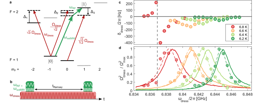
When driving the resonator at a frequency off-resonant to the atoms, the atomic transition is shifted by the MW field. This AC-Zeeman shift can be experimentally detected and used to reconstruct the intensity of the cavity field. We measure the frequency of the atomic transition between the magnetically trapped states and using time-domain Ramsey interferometry. The two states exhibit the same first-order Zeeman shift, thereby strongly reducing the sensitivity of the transition frequency to magnetic fields. For the Ramsey measurements, the atoms are prepared in a coherent superposition driven by a pulsed microwave field from an external antenna and an additional radio frequency fed to the Z-shaped trapping wire (green arrows in Fig. 2a). After a variable time , a second MW + RF pulse is applied and the relative population in the two states is measured. The populations in the two states oscillate with the difference between the atomic frequency and the external frequency, . During the Ramsey sequence, the coplanar microwave cavity is driven by a field with a variable angular frequency which is off-resonant to the atoms transition. This leads to an AC shift of the levels which depends on the detuning between and the atomic transition frequency. For a simple two-level system, the off-resonant field shifts the atomic states by , where denotes the Rabi frequency of the dressing field and is the detuning between the dressing field and the atomic transition frequency. The plus (minus) sign is valid for the ground (excited) state. The level scheme of the atoms involving all relevant fields is depicted in Fig. 2a. For a microwave field which is linearly polarized perpendicular to the quantization axis, as it is in our case, the cavity field induces and -transitions with equal field strength, as depicted by the red arrows. This field hence couples the state to the states and . The state , on the other hand, is coupled to state . This leads to a shift in the two-photon transition frequency by
| (1) |
which is measured in our experiment. Here, denotes the detuning to the relevant atomic hyperfine transition. The numerical factors in the numerator are determined by the Clebsch-Gordan coefficients of the transitions.
For the measurement, the power of the microwave fed to the resonator and the magnetic offset field ( mT) are held constant.
The measured frequency shift in the Ramsey experiment is shown in Fig. 2c. As visible in the curve measured at K, the dressing shift changes sign when the frequency of the dressing field is crossing an atomic resonance. Variation of the dressing frequency affects the shift in two ways, via the detuning to the atomic transitions and via a change in the microwave intensity in the resonator. Knowing the detuning to all involved levels, the normalized power of the microwave in the resonator, which is proportional to the square of the resonant Rabi frequency , can be deduced from the dressing shift. The calculated Rabi frequencies according to Eq. (1) are shown as circles in Fig. 2d. The measurement was repeated for different temperatures of the superconducting chip, corresponding to different cavity resonance frequencies. The result is compared with transmission spectra measured using a programmable network analyzer (solid lines in Fig. 2d). All curves are normalized to their maxima for the sake of comparability. Lorentzian curves (dashed lines) fitted to the data points match the transmission spectra closely in centre frequency and peak width, which is on the order of MHz. We attribute deviations in the peak positions to uncertainties in the temperature regulation of the cryostat, which are of the order mK.
Coherent control of atomic states with cavity fields
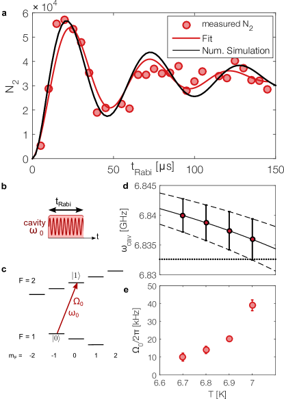
When the electromagnetic cavity field is resonant with one of the (allowed) atomic transitions, the atoms undergo coherent Rabi oscillations between the ground and excited state. The observation of these oscillations demonstrates coherent control over the internal atomic degrees of freedom. The Rabi frequency is given by , where is the atomic magnetic moment and is the amplitude of the oscillating magnetic microwave field. For the observation of these oscillations, we drive the cavity with a frequency GHz, which is in resonance with the atomic transition , but detuned roughly by twice the cavity linewidth from the cavity resonance ( GHz) at a chip temperature K. By state selective absorption imaging of the atoms, we observe resonant Rabi oscillations between the states and with a Rabi frequency kHz (Fig. 3a). By variation of the chip temperature between K and 7.0 K, the cavity frequency is shifted with respect to the atomic transition (Fig. 3d). This leads to a measurable change in the resonant Rabi frequency due to the altered MW power in the cavity, as visible in Fig. 3e. Here, the Rabi frequency increases with higher temperatures, as the cavity frequency approaches the atomic transition frequency. For temperatures around K, the cavity resonance is shifted to coincide with the atomic resonance. However, at this temperature, the critical current of the superconducting coupling inductances is too low to support a stable magnetic trap.
We observe a damping in the single-photon Rabi oscillations with a time constant of . This damping is a result of the dephasing due to the inhomogeneous MW field of the cavity and the fact that Rabi oscillations are driven between two states with different magnetic moments. The magnetically trapped state is subjected to an energy shift of MHz/mT, while the untrapped state is in first order insensitive to magnetic fields. As a consequence, the resonance frequency between the two states is not uniform across the cloud and the atoms are only exactly on resonance at the centre of the trap. A numerical simulation of a thermal cloud of trapped in a harmonic magnetic potential above the cavity gap shows a damping time in excellent agreement with our measurement.
In order to exploit the long coherence times of cold atoms, it is necessary to create superpositions between appropriate atomic states, which can both be trapped in the cavity. For 87Rb, such a state combination consists of the hyperfine levels and , which can both be trapped magnetically and exhibit excellent coherence properties. To this end, we start with an atomic cloud at a lower temperature of nK and atoms in the state .
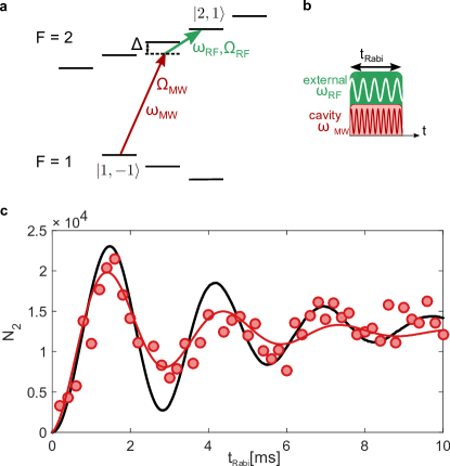
In order to prepare a coherent superposition of the two states, we drive the cavity with the MW field and employ an additional external RF field , with a detuning of kHz to the intermediate state (cf. Fig 4a). If the two corresponding Rabi frequencies are small compared to the intermediate detuning, i.e. , the population of the intermediate state can be neglected. In this case, the two-photon Rabi frequency can be calculated by adiabatic elimination of the intermediate state Gentile et al. (1989). By driving the two fields with variable pulse lengths, we observe Rabi oscillations with Hz, and a dephasing on the order of ms (Fig. 4c). A numerical simulation of an ensemble of non-interacting atoms in a magnetic trap reveals damping on the same timescale. As in the one-photon case, the dephasing is mainly due to the variation of the microwave field strength over the size of the atomic cloud (see Supplementary section S5).
Discussion
To make the presented cold atom-superconductor hybrid device a useful, high-coherence quantum resource, several aspects need to be addressed and optimized. In particular, dephasing during the Rabi pulses should be reduced and the coupling between atoms and the cavity increased.
Dephasing due to inhomogeneous coupling can, as seen in the experiment above, be a limitation for the high-fidelity creation of superposition states needed in information processing. The inhomogeneity seen by the atomic ensemble can be reduced by reducing the cloud temperature, yielding smaller cloud extension in the trap (see Supplementary section S5). Several experiments have furthermore shown that reliable superpositions or quantum gates can be achieved in spite of this temporal or spatial variation of Rabi frequencies, as the related dephasing can be overcome using more elaborate MW and RF pulses using optimal control theory Schulte-Herbrüggen et al. (2011); Dolde et al. (2014).
For our geometry, we have estimated the coupling between a single atom and a single cavity photon to be Hz. Various means can be used to increase the coupling strength between the atoms and the cavity field. By decreasing the width of the gap between the centre conductor and ground planes of the cavity, the magnetic field per photon could be increased according to , but would require the atoms to be trapped closer to the chip surface. By changing the resonator layout from CPW to lumped element resonator, the inductance and dimensions of the resonator could be decreased, leading to a significant enhancement of the current per photon and hence magnetic field . Finally, the electric field of the cavity mode could be used to couple neighbouring Rydberg states, exploiting the large electric dipole moments of Rydberg states Yu et al. (2016). A conservative estimate of the coupling between Rydberg atoms and the field of a higher harmonic mode for our geometry yields a coupling strength on the order of 1-2 MHz, which is on the same order as the cavity linewidth.
Conclusion
In summary, we have experimentally demonstrated coupling of ultracold ground state atoms to a driven superconducting coplanar waveguide resonator. Coupling was shown both in resonant Rabi oscillation and in dressing the frequency of an atomic clock state pair. Future measurements will explore collective effects of cold atoms to the cavity mode and work towards strong coupling between the superconducting resonator and Rydberg atoms. These experiments are the first step towards the implementation of cold atoms as a quantum resource in a hybrid quantum architecture.
Methods
Atomic cloud preparation
The atomic ensemble is prepared in a room-temperature setup and transported to a position below the superconducting atom chip using an optical dipole trap that is moved using a lens mounted on an air-bearing translation stage (cf. Ref. Cano et al. (2011) for details). Atoms are subsequently trapped in a magnetic trap generated by currents in the Z-shaped Nb wire and an external homogeneous bias field. The Z-wire configuration leads to a Ioffe-Pritchard-type magnetic microtrap with a non-zero offset field at the trap minimum. We load atoms at a temperature of into the magnetic chip trap. After adiabatic compression, the cloud is transferred into the mode volume of the resonator by rotating the external bias field and switching off the current in the Z-trap. Screening currents in the resonator, which conserve the flux in the closed superconducting loop, lead to the formation of a magnetic trap with oscillation frequencies s-1, s-1, s-1 below the gap of the waveguide cavity, from the chip surface. During the transfer into the tight trap, the atomic cloud is heated up to a temperature of . At the cavity position, we perform radiofrequency evaporation to further cool the atomic ensemble.
Experimental cycle and state selective detection
In order to measure the atomic state, the following experimental cycle is repeated every s. After preparation of an atomic cloud, transporting it to the superconducting chip and loading into the cavity, as described above, all atoms are in the hyperfine state . Subsequently, we apply one MW (+RF) pulse of variable length for the measurement of Rabi oscillations, or two -pulses of fixed length with a variable hold time in between for the Ramsey interferometry sequence. At the end of the sequence, we can measure the number of atoms in both of the states. First, the number of atoms in F=2 is measured by illuminating the cloud with light resonant to the transition. The shadow of the atoms is imaged on a CCD camera and the measured optical density is used to determine the atom number. We then pump the atoms from into by illumination with a laser resonant with the transition. From the state, the atoms decay into in ns and the atoms are imaged on a second CCD camera as described above.
References
- Xiang et al. (2013) Z.-L. Xiang, S. Ashhab, J. Q. You, and F. Nori, “Hybrid quantum circuits: Superconducting circuits interacting with other quantum systems,” Rev. Mod. Phys. 85, 623–653 (2013).
- André et al. (2006) A. André, D. Demille, J. M. Doyle, M. D. Lukin, S. E. Maxwell, P. Rabl, R. J. Schoelkopf, and P. Zoller, “A coherent all-electrical interface between polar molecules and mesoscopic superconducting resonators,” Nat. Phys. 2, 636–642 (2006).
- Henschel et al. (2010) K. Henschel, J. Majer, J. Schmiedmayer, and H. Ritsch, “Cavity QED with an ultracold ensemble on a chip: Prospects for strong magnetic coupling at finite temperatures,” Phys. Rev. A 82, 033810 (2010).
- Kim et al. (2011) Z. Kim, B. Suri, V. Zaretskey, S. Novikov, K. D. Osborn, A. Mizel, F. C. Wellstood, and B. S. Palmer, “Decoupling a Cooper-Pair Box to Enhance the Lifetime to 0.2 ms,” Phys. Rev. Lett. 106, 120501 (2011).
- Paik et al. (2011) H. Paik, D. I. Schuster, L. S. Bishop, G. Kirchmair, G. Catelani, A. P. Sears, B. R. Johnson, M. J. Reagor, L. Frunzio, L. I. Glazman, S. M. Girvin, M. H. Devoret, and R. J. Schoelkopf, “Observation of High Coherence in Josephson Junction Qubits Measured in a Three-Dimensional Circuit QED Architecture,” Phys. Rev. Lett. 107, 240501 (2011).
- Verdú et al. (2009) J. Verdú, H. Zoubi, C. Koller, J. Majer, H. Ritsch, and J. Schmiedmayer, “Strong Magnetic Coupling of an Ultracold Gas to a Superconducting Waveguide Cavity,” Phys. Rev. Lett. 103, 043603 (2009).
- Patton and Fischer (2013a) K. R. Patton and U. R. Fischer, “Hybrid of superconducting quantum interference device and atomic Bose-Einstein condensate: An architecture for quantum information processing,” Phys. Rev. A 87, 052303 (2013a).
- Patton and Fischer (2013b) K. R. Patton and U. R. Fischer, “Ultrafast Quantum Random Access Memory Utilizing Single Rydberg Atoms in a Bose-Einstein Condensate,” Phys. Rev. Lett. 111, 240504 (2013b).
- Kubo et al. (2010) Y. Kubo, F. R. Ong, P. Bertet, D. Vion, V. Jacques, D. Zheng, A. Dréau, J.-F. Roch, A. Auffeves, F. Jelezko, J. Wrachtrup, M. F. Barthe, P. Bergonzo, and D. Esteve, “Strong Coupling of a Spin Ensemble to a Superconducting Resonator,” Phys. Rev. Lett. 105, 140502 (2010).
- Kubo et al. (2011) Y. Kubo, C. Grezes, A. Dewes, T. Umeda, J. Isoya, H. Sumiya, N. Morishita, H. Abe, S. Onoda, T. Ohshima, V. Jacques, A. Dréau, J.-F. Roch, I. Diniz, A. Auffeves, D. Vion, D. Esteve, and P. Bertet, “Hybrid Quantum Circuit with a Superconducting Qubit Coupled to a Spin Ensemble,” Phys. Rev. Lett. 107, 220501 (2011).
- Amsüss et al. (2011) R. Amsüss, C. Koller, T. Nöbauer, S. Putz, S. Rotter, K. Sandner, S. Schneider, M. Schramböck, G. Steinhauser, H. Ritsch, J. Schmiedmayer, and J. Majer, “Cavity QED with Magnetically Coupled Collective Spin States,” Phys. Rev. Lett. 107, 060502 (2011).
- Putz et al. (2014) S. Putz, D. O. Krimer, R. Amsüss, A. Valookaran, T. Nöbauer, J. Schmiedmayer, S. Rotter, and J. Majer, “Protecting a spin ensemble against decoherence in the strong-coupling regime of cavity QED,” Nat. Phys. 10, 720–724 (2014).
- Grezes et al. (2016) C. Grezes, Y. Kubo, B. Julsgaard, T. Umeda, J. Isoya, H. Sumiya, H. Abe, S. Onoda, T. Ohshima, K. Nakamura, I. Diniz, A. Auffeves, V. Jacques, J.-F. Roch, D. Vion, D. Esteve, K. Moelmer, and P. Bertet, “Towards a spin-ensemble quantum memory for superconducting qubits,” Comptes Rendus Physique 17, 693 – 704 (2016).
- Schuster et al. (2010) D. I. Schuster, A. P. Sears, E. Ginossar, L. DiCarlo, L. Frunzio, J. J. L. Morton, H. Wu, G. A. D. Briggs, B. B. Buckley, D. D. Awschalom, and R. J. Schoelkopf, “High-Cooperativity Coupling of Electron-Spin Ensembles to Superconducting Cavities,” Phys. Rev. Lett. 105, 140501 (2010).
- Probst et al. (2013) S. Probst, H. Rotzinger, S. Wünsch, P. Jung, M. Jerger, M. Siegel, A. V. Ustinov, and P. A. Bushev, “Anisotropic rare-earth spin ensemble strongly coupled to a superconducting resonator,” Phys. Rev. Lett. 110, 157001 (2013).
- Petrosyan et al. (2009) D. Petrosyan, G. Bensky, G. Kurizki, I. Mazets, J. Majer, and J. Schmiedmayer, “Reversible state transfer between superconducting qubits and atomic ensembles,” Phys. Rev. A 79, 040304 (2009).
- Petrosyan and Fleischhauer (2008) D. Petrosyan and M. Fleischhauer, “Quantum Information Processing with Single Photons and Atomic Ensembles in Microwave Coplanar Waveguide Resonators,” Phys. Rev. Lett. 100, 170501 (2008).
- Pritchard et al. (2014) J. D. Pritchard, J. A. Isaacs, M. A. Beck, R. McDermott, and M. Saffman, “Hybrid atom-photon quantum gate in a superconducting microwave resonator,” Phys. Rev. A 89, 010301 (2014).
- Sárkány, Fortágh, and Petrosyan (2015) L. Sárkány, J. Fortágh, and D. Petrosyan, “Long-range quantum gate via Rydberg states of atoms in a thermal microwave cavity,” Phys. Rev. A 92, 030303 (2015).
- Hafezi et al. (2012) M. Hafezi, Z. Kim, S. L. Rolston, L. A. Orozco, B. L. Lev, and J. M. Taylor, “Atomic interface between microwave and optical photons,” Phys. Rev. A 85, 020302 (2012).
- Yu et al. (2017) D. Yu, L. C. Kwek, L. Amico, and R. Dumke, “Theoretical description of a micromaser in the ultrastrong-coupling regime,” Phys. Rev. A 95, 053811 (2017).
- Haroche and Raimond (2006) S. Haroche and J. Raimond, Exploring the Quantum: Atoms, Cavities, and Photons, Oxford graduate texts in mathematics (OUP Oxford, 2006).
- Wallraff et al. (2004) A. Wallraff, D. Schuster, A. Blais, L. Frunzio, R. Huang, J. Majer, S. Kumar, S. Girvin, and R. Schoelkopf, “Strong coupling of a single photon to a superconducting qubit using circuit quantum electrodynamics,” Nature 431, 162–167 (2004).
- DiCarlo et al. (2010) L. DiCarlo, M. D. Reed, L. Sun, B. R. Johnson, J. M. Chow, J. M. Gambetta, L. Frunzio, S. M. Girvin, M. H. Devoret, and R. J. Schoelkopf, “Preparation and measurement of three-qubit entanglement in a superconducting circuit,” Nature 467, 574–578 (2010).
- Lucero et al. (2012) E. Lucero, R. Barends, Y. Chen, J. Kelly, M. Mariantoni, A. Megrant, P. O’Malley, D. Sank, A. Vainsencher, J. Wenner, T. White, Y. Yin, A. N. Cleland, and J. M. Martinis, “Computing prime factors with a Josephson phase qubit quantum processor,” Nat. Phys. 8, 719–723 (2012).
- Treutlein et al. (2004) P. Treutlein, P. Hommelhoff, T. Steinmetz, T. W. Hänsch, and J. Reichel, “Coherence in Microchip Traps,” Phys. Rev. Lett. 92, 203005 (2004).
- Deutsch et al. (2010) C. Deutsch, F. Ramirez-Martinez, C. Lacroûte, F. Reinhard, T. Schneider, J. N. Fuchs, F. Piéchon, F. Laloë, J. Reichel, and P. Rosenbusch, “Spin Self-Rephasing and Very Long Coherence Times in a Trapped Atomic Ensemble,” Phys. Rev. Lett. 105, 020401 (2010).
- Kleine Büning et al. (2011) G. Kleine Büning, J. Will, W. Ertmer, E. Rasel, J. Arlt, C. Klempt, F. Ramirez-Martinez, F. Piéchon, and P. Rosenbusch, “Extended Coherence Time on the Clock Transition of Optically Trapped Rubidium,” Phys. Rev. Lett. 106, 240801 (2011).
- Dudin, Li, and Kuzmich (2013) Y. O. Dudin, L. Li, and A. Kuzmich, “Light storage on the time scale of a minute,” Phys. Rev. A 87, 031801 (2013).
- Bernon et al. (2013) S. Bernon, H. Hattermann, D. Bothner, M. Knufinke, P. Weiss, F. Jessen, D. Cano, M. Kemmler, R. Kleiner, D. Koelle, and J. Fortágh, “Manipulation and coherence of ultra-cold atoms on a superconducting atom chip,” Nat. Commun. 4, 2380 (2013), 10.1038/ncomms3380.
- Nirrengarten et al. (2006) T. Nirrengarten, A. Qarry, C. Roux, A. Emmert, G. Nogues, M. Brune, J.-M. Raimond, and S. Haroche, “Realization of a Superconducting Atom Chip,” Phys. Rev. Lett 97, 200405 (2006).
- Mukai et al. (2007) T. Mukai, C. Hufnagel, A. Kasper, T. Meno, A. Tsukada, K. Semba, and F. Shimizu, “Persistent Supercurrent Atom Chip,” Phys. Rev. Lett 98, 260407 (2007).
- Roux et al. (2008) C. Roux, A. Emmert, A. Lupascu, T. Nirrengarten, G. Nogues, M. Brune, J. M. Raimond, and S. Haroche, “Bose-Einstein condensation on a superconducting atom chip,” Europhys. Lett. 81, 56004 (2008).
- Minniberger et al. (2014) S. Minniberger, F. Diorico, S. Haslinger, C. Hufnagel, C. Novotny, N. Lippok, J. Majer, C. Koller, S. Schneider, and J. Schmiedmayer, “Magnetic conveyor belt transport of ultracold atoms to a superconducting atomchip,” Appl. Phys. B 116, 1017–1021 (2014).
- Müller et al. (2010) T. Müller, B. Zhang, R. Fermani, K. S. Chan, M. J. Lim, and R. Dumke, “Programmable trap geometries with superconducting atom chips,” Phys. Rev. A 81, 053624 (2010).
- Weiss et al. (2015) P. Weiss, M. Knufinke, S. Bernon, D. Bothner, L. Sárkány, C. Zimmermann, R. Kleiner, D. Koelle, J. Fortágh, and H. Hattermann, “Sensitivity of ultracold atoms to quantized flux in a superconducting ring,” Phys. Rev. Lett. 114, 113003 (2015).
- Sárkány et al. (2014) L. Sárkány, P. Weiss, H. Hattermann, and J. Fortágh, “Controlling the magnetic-field sensitivity of atomic-clock states by microwave dressing,” Phys. Rev. A 90, 053416 (2014).
- Bothner et al. (2017) D. Bothner, D. Wiedmaier, B. Ferdinand, R. Kleiner, and D. Koelle, “Improving superconducting resonators in magnetic fields by reduced field-focussing and engineered flux screening,” arXiv:1707.01936 (2017).
- Bothner et al. (2013) D. Bothner, M. Knufinke, H. Hattermann, R. Wölbing, B. Ferdinand, P. Weiss, S. Bernon, J. Fortágh, D. Koelle, and R. Kleiner, “Inductively coupled superconducting half wavelength resonators as persistent current traps for ultracold atoms,” New J. Phys. 15, 093024 (2013).
- Chiorescu et al. (2010) I. Chiorescu, N. Groll, S. Bertaina, T. Mori, and S. Miyashita, “Magnetic strong coupling in a spin-photon system and transition to classical regime,” Phys. Rev. B 82, 024413 (2010).
- Gentile et al. (1989) T. R. Gentile, B. J. Hughey, D. Kleppner, and T. W. Ducas, “Experimental study of one- and two-photon Rabi oscillations,” Phys. Rev. A 40, 5103–5115 (1989).
- Schulte-Herbrüggen et al. (2011) T. Schulte-Herbrüggen, A. Spörl, N. Khaneja, and S. J. Glaser, “Optimal control for generating quantum gates in open dissipative systems,” J. Phys B: At., Mol. and Opt. Phys. 44, 154013 (2011).
- Dolde et al. (2014) F. Dolde, V. Bergholm, Y. Wang, I. Jakobi, B. Naydenov, S. Pezzagna, J. Meijer, F. Jelezko, P. Neumann, T. Schulte-Herbrüggen, J. Biamonte, and J. Wrachtrup, “High-fidelity spin entanglement using optimal control,” Nat. Commun. 5, 3371 (2014).
- Yu et al. (2016) D. Yu, M. M. Valado, C. Hufnagel, L. C. Kwek, L. Amico, and R. Dumke, “Charge-qubit–atom hybrid,” Phys. Rev. A 93, 042329 (2016).
- Cano et al. (2011) D. Cano, H. Hattermann, B. Kasch, C. Zimmermann, R. Kleiner, D. Koelle, and J. Fortágh, “Experimental system for research on ultracold atomic gases near superconducting microstructures,” Eur. Phys. J. D 63, 17–23 (2011).
Acknowledgements
This work was supported by the Deutsche Forschungsgemeinschaft (SFB TRR21) and the European Commission (FP7 STREP project “HAIRS”). H.H. and B.F. acknowledge additional support from the Carl Zeiss Stiftung and the Research Seed Capital (RiSC) programme of the MWK Baden-Württemberg.
Author contributions
D.K., R.K., J.F., and H.H. designed and mounted the experiment. D.B., D.W., B.F. and H.H. developed and fabricated the superconducting chip. H.H. and L.Y.L. carried out the experiments, H.H.,D.B., L.Y.L. and B.F. analyzed the data. H.H., D.B. and B.F. performed the numerical simulations. L.S. provided the microwave dressing theory. D.K., R.K. and J.F. supervised the project. H.H., D.B. and J.F. edited the manuscript. All authors discussed the results and contributed to the manuscript.
Competing financial interest
The authors declare no competing financial interests.
Supplementary Materials: Coupling ultracold atoms to a superconducting coplanar waveguide resonator
H. Hattermann, D. Bothner, L. Y. Ley, B. Ferdinand, D. Wiedmaier, L. Sárkány, R. Kleiner, D. Koelle, J. Fortágh
CQ Center for Quantum Science in LISA+, Physikalisches Institut, Eberhard Karls Universität Tübingen, Auf der Morgenstelle 14, D-72076 Tübingen, Germany
S1 Atom chip design and fabrication
Our atom chip combines two structures, a m wide Z-shaped superconducting Nb strip for the application of directed and low frequency currents as well as a superconducting coplanar waveguide resonator with a resonance frequency of GHz, near-resonant with the ground state hyperfine transition frequency of 87Rb atoms. All structures are patterned onto a m thick sapphire substrate by means of optical lithography, thin film deposition and microfabrication . A schematic of the atom trapping region on the chip is shown in Fig. S1a and a cross-sectional view along the dotted line in S1a is shown in S1b. The full chip layout is shown in Fig. 1a of the main paper.
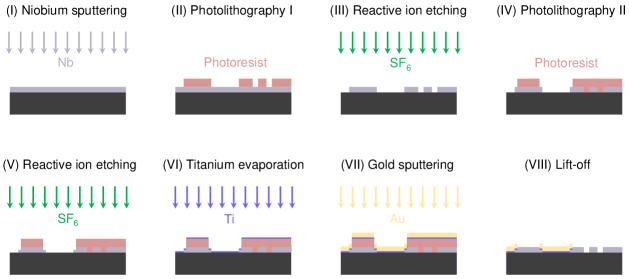
The coplanar microwave resonator has a centre conductor width of m and two ground planes, which are separated from the centre conductor by a gap of m, targeting a characteristic impedance . In order to facilitate the magnetic trapping of atoms closely above the gaps of the waveguide structure, the magnetic field distorting superconducting ground planes had to be removed partially. As we observe strong parasitic resonances when parts of the ground planes are missing (probably due to a parasitic mutual inductance between the trapping wire and the waveguide structure and due to the excitation of chip resonances), we substituted the removed superconducting parts by a normal-conducting Au metallization layer, restoring a good ground connection along the whole resonator. Thus, the trapping wire is embedded into one of the ground planes and galvanically connected to all metallization parts on the chip. As superconductor we use niobium, and as normal conductor we use gold on top of a thin adhesion layer of titanium. The thicknesses of the three films are nm, nm, and nm, cf. Fig. S1b. Between the superconducting parts and the normal-conducting parts, there is a m wide overlap region, ensuring a low contact resistance.
In order to minimize additional microwave losses induced by the presence of the normal conductor, we only replaced the superconductor by gold in the trapping region ( of the total resonator length) and kept also a m part of the ground plane in this region superconducting. The normal conducting region in between this remaining superconducting part of the ground plane and the superconducting trapping wire is m wide, cf. Fig. S1b.

The device fabrication is schematically shown in Fig. S2. It starts with the DC magnetron sputtering of the Nb onto a bare r-cut Sapphire substrate. By means of optical lithography and SF6 reactive ion etching, we pattern the superconducting parts. Next, we cover most of the superconducting parts – except for the m wide overlap region – with photoresist and deposit the normal conducting metal on top. To do so, we first remove nm of the Nb in the overlap region by another SF6 reactive ion etching step in order to get rid of photoresist residues and a possible native oxide layer on top of the Nb and in addition to reduce the substrate-Nb step height. Then, we in-situ deposited the Ti adhesion layer by means of electron beam evaporation and the Au layer by DC magnetron sputtering. We finalized the fabrication by lifting off the normal conducting parts in hot acetone supported by ultrasound.
S2 Cavity parameters
The microwave resonator used in this experiment is a half wavelength () transmission line cavity based on a coplanar waveguide with charactersitic impedance and attenuation constant . The transmission line cavity has a length mm and a fundamental mode resonance frequency GHz at a temperature of K. Around its resonance frequency, the waveguide resonator can be modelled as an inductively coupled series RLC circuit, cf. Fig. S3a and S3b with the equivalent lumped element resistance , inductance and capacity Bothner et al. (2013):
| (S1) |
where is the attenuation constant of the coplanar waveguide and is the ”uncoupled” resonance frequency, i.e., the resonance frequency corresponding only to the electrical length of the cavity.
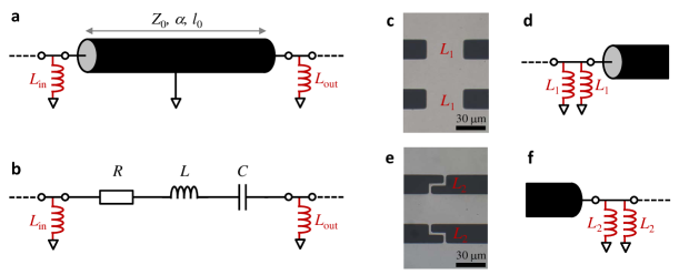
For driving the resonator and reading out its frequency dependent response, the cavity is weakly coupled to two feedlines by shunt inductors between the centre conductor and the ground planes at both ends, cf. Fig. 1 of the main paper. The shunt inductors at the input port are shown in Fig. S3c. Each of the two superconducting shunts to ground is m wide and m long. With the software package 3D-MLSI Khapaev et al. (2003), we determined each of the two shunt inductances to be pH, giving a total input port coupling inductance pH.
At the output port, cf. Fig. S3e, the shunt inductors are m wide and m long, giving an inductance per shunt of pH. Thus, the total inductance at the output port is pH.
For the resonance frequency of the coupled circuit is shifted due to the coupling inductors according to
| (S2) |
The external linewidth of the resonator due to losses through the input port is given by Bothner et al. (2013)
| (S3) |
For the output port, we find
| (S4) |
These linewidths correspond to a total external linewidth
| (S5) |
or a total external quality factor
| (S6) |
In liquid helium, at temperature K, we measure a total quality factor of , indicating that the majority of the losses is due to thermal quasiparticles in the superconductor as well as due to dissipation in the normal conducting parts and the interfaces between the different metals.
S3 Cavity temperature dependence
S3.1 Temperature calibration
The magnetic penetration depth in a BCS superconductor shows a temperature dependence, which can be approximately captured by Tinkham (2004)
| (S7) |
with the sample temperature and the superconducting transition temperature . The origin of this temperature dependence is the temperature dependence of the superconducting charge carrier density.
The total inductance of a superconducting resonator is given by the sum of the temperature independent geometric inductance and the kinetic inductance, , which takes into account the kinetic energy of the superconducting charge carriers. For superconductors with a thickness larger than twice the penetration depth, the kinetic inductance is related to the magnetic penetration depth via
| (S8) |
where is a geometrical factor, taking into account the spatial distribution of the superconducting current density. In our samples, we have nm and typically nm. Thus, up to , which is much larger than all values of in our experiment, is fulfilled.
In general, also the coupling inductors have a kinetic contribution, but due to in our device, we neglect this small correction here. With the temperature dependent kinetic inductance, the resonance frequency is given by
| (S9) |
where is the inductance of the cavity without the kinetic contribution and is the resonance frequency for (not for ).
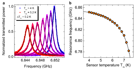
In our experiment, we take advantage of the temperature dependence of the cavity resonance frequency to tune it close to the atomic transition frequency. Figure S4a shows (smoothed) transmission spectra for different temperatures measured with the sensor mounted to the helium flow cryostat, which also hosts the chip. We observe the resonance frequency shifting towards lower values with increasing temperature. In Fig. S4b, we plot the extracted resonance frequency vs the measured temperature .
As the thermometer is positioned inside the coldfinger of the flow cryostat cm from the chip itself, we expect the sample temperature to be different from the sensor temperature by an offset temperature , i.e.,
| (S10) |
We note that we use a calibrated sensor and thus that the offset is not related to uncertainty of the sensor measurement, but due to the nature of the setup Cano et al. (2010). The chip and the microwave amplifier are mounted on a cm high sample holder of oxygen-free high-conductivity copper. The cooling power of the chip is mainly limited by the thermal conductivity through the interfaces between the cryostat and the chip holder and between chip holder and the sapphire chip. Due to the requirement to have optical access to the chip region, mm high slits have been cut into the thermal shield at K, which encloses the coldfinger tip and the sample holder in order to minimize the thermal radiation from the room temperature environment. The final temperature of the chip is given by a combination of the cooling power from the coldfinger and the heating power due to thermal radiation from the environment. We find a very good agreement between the experimentally determined resonance frequencies shown in Fig. S4b, the transition temperature of our Nb K and Eq. (S9) when we assume K, GHz and a kinetic inductance participation ratio . The result is shown as black line in Fig. S4b and gives us a rough estimate for the temperature offset between sample and sensor.
S3.2 Temperature fine calibration and full cavity characterization
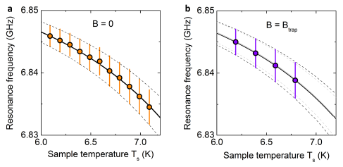
As the offset temperature is not exactly constant between 5 K and 9 K and as all our experiments are done within a limited temperature window of K, we performed a more detailed cavity characterization in the corresonding temperature interval. The results of this detailed cavity characterization are shown in Fig. S5. In Fig. S5a, we plot the resonance frequency vs the sample temperature, where the sample temperature was determined from the analytical approximation shown as black line. To achieve the best match in this temperature region, we had to adjust the offset temperature to K, but kept all other parameters used above.
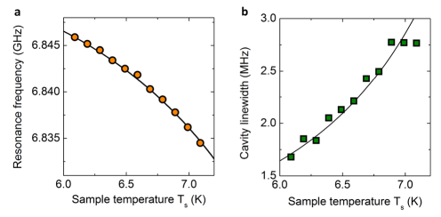
In addition to the resonance frequency, we also extracted the resonance linewidth for each temperature, which is shown in Fig. S5b. From the two-fluid model Buckel and Kleiner (2004); Tinkham (2004), it follows that the surface resistance of a superconductor is given by
| (S11) |
where is the real part of the complex two-fluid conductivity with the quasiparticle density and the total electron density . From the temperature dependence of and the two-fluid model, the temperature dependence of the superconducting charge carrier density is given by
| (S12) |
This leads to the quasiparticle density fraction
| (S13) |
Taking the relation for the quasiparticle induced losses and assuming , which for this consideration is reasonable as their relative change is only , we get as cavity linewidth temperature dependence
| (S14) |
with a temperature independent contribution and the scaling factor . Figure S5b shows an approximation to the data using this expression with kHz and MHz (K) as lines.
S3.3 Influence of the magnetic trapping fields
Applying an external magnetic field can shift the cavity frequency as well as the cavity linewidth due to Meissner screening currents Healey et al. (2008) and the presence of Abrikosov vortices Song et al. (2009); Bothner et al. (2012). In our experiment, we apply only small fields in the T range, but due to the fact that we also apply a field during the transition to the superconduting state, we will trap some vortices in the cavity leads Stan et al. (2004). As the magnetic field distribution including vortices is very complicated for our device, we describe the field-induced property shifts phenomenologically by slightly adjusting the kinetic inductance participation ratio and the parameter .
In Fig. S6a, we plot the zero magnetic field data points and the analytic expressions (lines) as derived in the previous section and in S6b we show the experimental data obtained within the full magnetic trapping field configuration. For comparison, we also plot the lines of S6a in S6b, but in grey, demonstrating that the magnetic fields indeed lead to a small resonance frequency downshift and a slight increase of the linewidth. Both effects can be captured by using and . The result is shown as black dashed lines in S6b and is in excellent agreement with the data.
S4 Magnetic field simulations
The magnetic field simulations in this work have been performed using the software package 3D-MLSI Khapaev et al. (2003). For the calculations of the RF magnetic field, simplified versions of our real chip were used, as the full structure was too large to be computed to the full extent. We do not expect the modifications (e.g. shortening the Z-shaped trapping wire to the trapping region), however, to have a significant impact onto the final results.
S4.1 Coupling per photon and atom
The microwave current of the fundamental mode along the resonator is given by
| (S15) |
where is the coordinate along the resonator starting from the input port with , mm is the resonance wavelength and is the amplitude in the current antinodes. To calculate the coupling rate between a single photon and a single atom in the cavity, we estimate the zero point fluctuations of the microwave current in the resonator and at the position of the atoms (current antinode) by
| (S16) | |||||
| (S17) |
where the inductance per unit length is nH/m (kinetic inductance contributions are neglected here due to their smallness) and is the root mean square of the zero point fluctuation amplitude . With GHz and mm we get
| (S18) |
To relate this to the coupling, we calculate the magnetic field related to this current at the position of the atoms by means of finite element simulations using the software package 3D-MLSI Khapaev et al. (2003).
Finally, we take into account the position of the atomic cloud along the resonator, which reduces the effective magnetic field to . Figure S7 shows the magnetic microwave field zero point fluctuations obtained from these simulations in a cross-section of the coplanar waveguide at the position of the atoms.
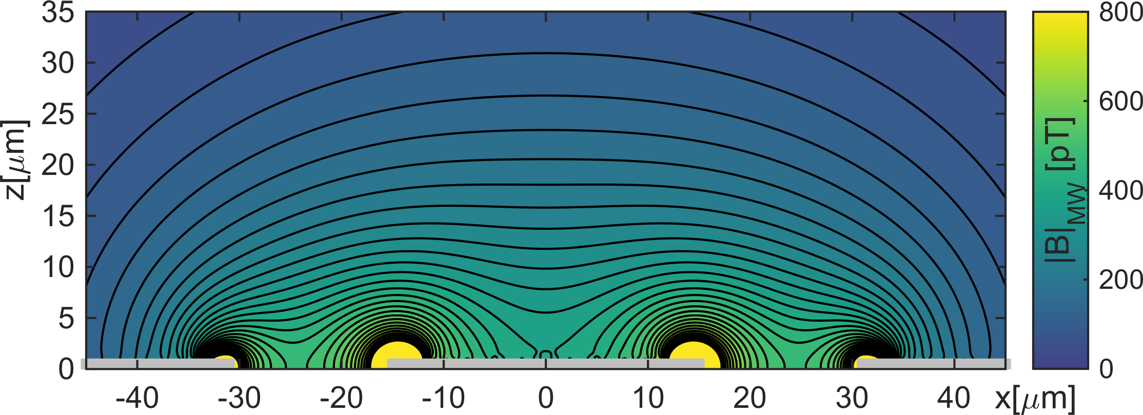
From the magnetic microwave field, we calculate the single-atom coupling rate as
| (S19) |
with the magnitude of the dipole transition matrix element . The result is shown in Fig. 1f of the main paper.
S4.2 The radio-frequency magnetic field
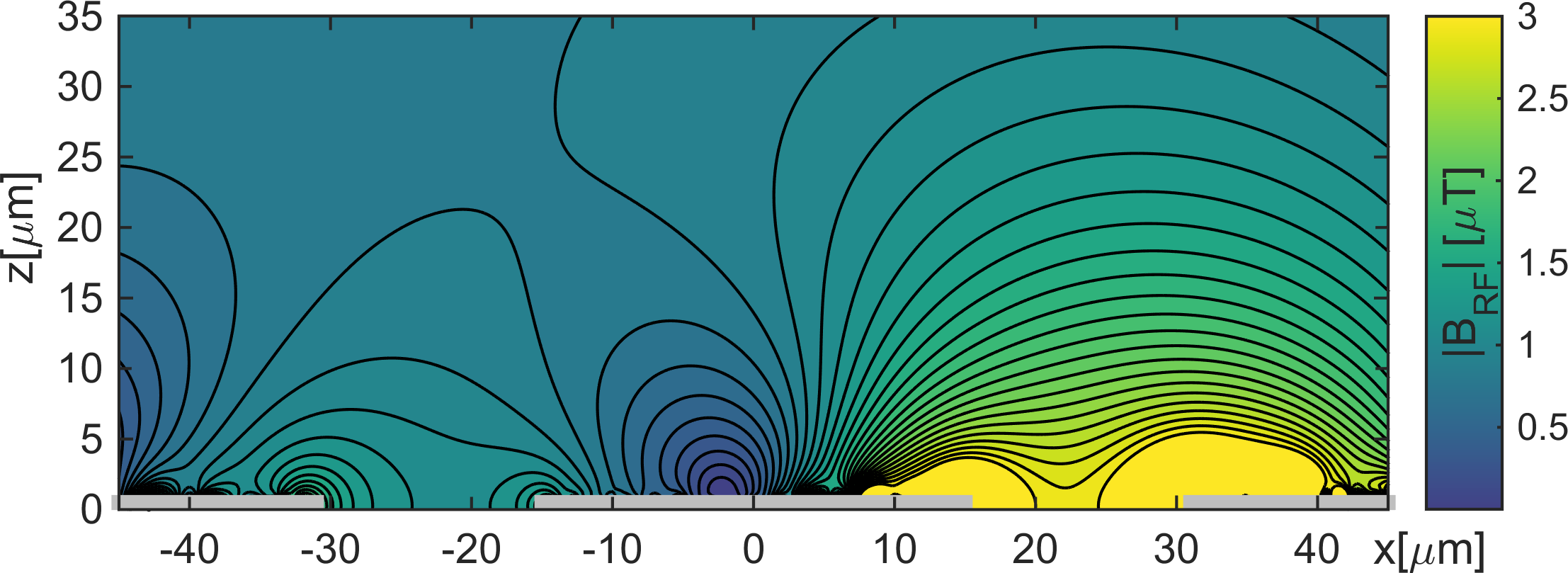
For the two-photon experiments and the corresponding simulations, we also need the magnetic field of the radio-frequency (RF) current, which is sent through the Z-shaped trapping wire. Thus, we calculate the magnetic field for a current of mA on the trapping wire and show the result at the position of the atoms in Fig. S8.
S5 Simulated Rabi oscillations in the cavity
S5.1 One photon Rabi oscillations
Numerical simulations of the coherent Rabi oscillations of atomic ensembles in the cavity yield further insight into the observed dephasing rates. We assume a thermal ensemble of atoms with a temperature of nK trapped in a harmonic magnetic trap with s-1, s-1, s-1. The centre of the trap is assumed m from the chip surface, as depicted in Fig. 1f in the main article.
For the one-photon Rabi oscillation, the Rabi frequency is much higher than the oscillation frequency of the atoms in the trapping potential, i.e. . We therefore can assume a static Gaussian density distribution of atoms in the trap, and use a total atom number of atoms for the simulations. We use the numerically calculated field strength depicted in Fig. S7, multiplied by a constant numerical factor to match the observed Rabi oscillation frequency. For each position , the probability to find atoms in the excited state is computed as
| (S20) |
where is the generalized Rabi frequency, and the magnetic-field dependent detuning of the microwave to the atomic transition. The probability is multiplied with the local atomic density and summation over all atoms yields the total atom number in the excited state. The simulated results closely match the observed dephasing of the Rabi oscillations, as seen in Fig. 3a in the main paper.
S5.2 Two-photon Rabi oscillations
For the simulated two-photon Rabi oscillations, we assume a three level system of states , , and .
States and are coupled by the cavity microwave field with the Rabi frequency . An additional radio frequency couples the state to the state . Both the microwave and the radio frequency field are detuned to the transition to the intermediate state by the detuning , c.f. Fig. 5b in the main article. The inhomogeneity of the cavity field is the same as for the one-photon case above. The spatial dependence of the radio-frequency field is simulated with the software package 3D-MLSI by applying a current in the Z-shaped wire and calculating the Meissner screening currents close to the resonator, c.f. S8. As the effective Rabi frequency is much lower as in the one-photon case, the assumption of static atoms no longer holds. The motion of atoms through the spatially inhomogeneous MW and RF field leads to a time dependence of the Rabi frequency seen by each atom.
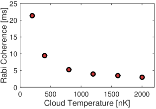
To account for this, we randomly initialize 5000 non-interacting particles in the state in the harmonic potential with a distribution corresponding to a temperature of 800 nK. We then simulate the movement of the atoms through the potential and the evolution of the three states with a Runge-Kutta calculation of fourth order. Stability of the simulations was ensured by changing the time steps in the calculations. The main source of the dephasing in the Rabi oscillations is the inhomogeneity of the MW field. This can be seen from simulations with colder and thus smaller clouds, as visible in Fig. S9.
.
References
- Bothner et al. (2013) D. Bothner, M. Knufinke, H. Hattermann, R. Wölbing, B. Ferdinand, P. Weiss, S. Bernon, J. Fortágh, D. Koelle, and R. Kleiner, Inductively coupled superconducting half wavelength resonators as persistent current traps for ultracold atoms, New J. Phys. 15, 093024 (2013)
- Khapaev et al. (2003) M. M. Khapaev, M. Y. Kupriyanov, E. Goldobin, and M. Siegel, Current distribution simulation for superconducting multi-layered structures, Supercond. Sci. Technol. 16, 24 (2003)
- Tinkham (2004) \BibitemOpen\bibfieldauthor M. Tinkham, Introduction to Superconductivity: Second Edition, Dover Books on Physics (Dover Publications, 2004)
- Cano et al. (2010) D. Cano, H. Hattermann, B. Kasch, C. Zimmermann, R. Kleiner, D. Koelle, and J. Fortágh, Experimental system for research on ultracold atomic gases near superconducting microstructures, Eur. Phys. J. D 63, 17 (2010)
- Buckel and Kleiner (2004) \BibitemOpen\bibfieldauthor W. Buckel and R. Kleiner, Superconductivity: fundamentals and applications (Wiley-VCH, 2004)
- Healey et al. (2008) J. E. Healey, T. Lindström, M. S. Colclough, C. M. Muirhead, and A. Ya. Tzalenchuk, Magnetic field tuning of coplanar microwave resonators, Appl. Phys. Lett. 93, 043513 (2008)
- Song et al. (2009) C. Song, T. W. Heitmann, M. P. DeFeo, K. Yu, R. McDermott, M. Neeley, J. M. Martinis, and B. L. T. Plourde, Microwave response of vortices in superconducting thin films of Re and Al, Phys. Rev. B 79, 174512 (2009a)
- Bothner et al. (2012) D. Bothner, T. Gaber, M. Kemmler, D. Koelle, R. Kleiner, S. Wünsch, and M. Siegel, Magnetic hysteresis effects in superconducting coplanar microwave resonators, Phys. Rev. B 86, 014517 (2012)
- Stan et al. (2004) G. Stan, S. B. Field, and J. M. Martinis, Critical field for complete vortex expulsion from narrow superconducting strips, Phys. Rev. Lett. 92, 097003 (2004)