Long-range non-Coulombic electron-electron interactions between LaAlO3/SrTiO3 nanowires
Abstract
The LaAlO3/SrTiO3 system exhibits unusual magnetic and superconducting behavior arising from electron-electron interactions whose physical origin is not well understood. Quantum transport techniques, especially those involving mesoscopic geometries, can offer insight into these interactions. Here we report evidence for long-range electron-electron interactions in LaAlO3/SrTiO3 nanowires, measured through the phenomenon of frictional drag, in which current passing through one nanowire induces a voltage across a nearby electrically isolated nanowire. Frictional drag mediated by the Coulomb interaction is predicted to decay exponentially with interwire separation, but with the LaAlO3/SrTiO3 nanowire system it is found to be nearly independent of separation. Frictional drag experiments performed with three parallel wires demonstrates long-range frictional coupling even in the presence of an electrically grounded central wire. Collectively, these results provides evidence for a new long-range non-Coulombic electron-electron interaction unlike anything previously reported for semiconducting systems.
The heterointerface between the complex oxides LaAlO3 and SrTiO3 (LAO/STO) Ohtomo2004 exhibits a rich variety of electronically-tunable properties such as superconductivity Caviglia2007 ; Caviglia2008 , magnetism brinkman2007 ; pai2016 , and spin-orbit coupling Shalom2010 ; Caviglia2010 . Many of these properties have been associated with strong gate-tunable electron-electron interactions Cheng2015 ; Cheng2016 which can be challenging to dissect using conventional transport methods. The LAO/STO interface also exhibits a hysteretic metal-insulator transition Thiel2006 , which can be controlled locally using conductive atomic force microscopy (c-AFM) lithography ChengCen2008 ; ChengCen2009 and used to create a range of mesoscopic devices Sulpizio2014 .
The transport technique of Coulomb drag Narozhny2016 (or more generally “frictional drag”) can provide unique insight into electron-electron interactions in the LAO/STO system. When two electrical conductors are situated in close proximity, current driven through one (the “drive”) conductor may induce a voltage (or current) in the second (“drag”) conductor. This effect was first proposed by Pogrebinskii Progrebinskii1977 as a method to probe correlations among the charge carriers of the system. Frictional drag measurements have been carried out in coupled 2D-3D semiconductor systems Solomon1989 ; Solomon1991 , coupled semiconductor 2DEGs Gramila1991 ; Gramila1992 ; Gramila1994 ; Solomon1991 ; Eisenstein1992 and graphene Li2016 ; Lee2016 systems, 1D-1D nanowires defined from semiconductor 2DEGs Debray2001 ; Tokura2006 ; Laroche2014 , and in coupled semiconductor quantum dots Keller2016 . In these systems, the physical mechanism underlying frictional drag is dominated by Coulomb interactions. At large separations, non-Coulombic corrections can become apparent in some semiconductor devices Gramila1993 ; Tso1992 ; Tso1994 .
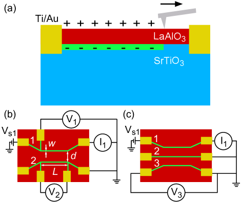
Here we report frictional drag measurements performed on LAO/STO nanowire-based devices. The device fabrication process is illustrated in Fig. 1(a). C-AFM lithography is used to define nanowires at the interface between 3.4 unit cells (uc) of LAO deposited on an STO substrate by pulsed laser deposition (PLD). Details of the sample growth and fabrication of electrical contacts are described elsewhere WaterCycle ; ChengCen2008 . Positive tip voltages applied on the LAO surface produce locally conductive regions at the LAO/STO interface. The mechanism for the writing process is attributed to surface protonation WaterCycle ; Bi2010 . A typical frictional drag system (illustrated in Fig. 1(b)) is composed of two parallel nanowires with a width nm, length ranging between 400 nm and 1.5 m, and separation ranging between nm and 1.5 m. Devices consisting of three parallel nanowires (shown in Fig. 1(c)) are also investigated. Except where noted otherwise, all measurements are performed below 100 mK. In both double-wire (Fig. 1(b)) and triple-wire (Fig. 1(c)) device geometries, frictional drag measurements are performed by sourcing a current in nanowire and measuring an induced voltage in nanowire . All nanowires are connected to the same ground during the measurement. The current is produced by applying a voltage to one end of nanowire ; the resulting current and induced voltage at frequency are measured using a lock-in amplifier. The resistance may then be expressed as a matrix , which is generally a function of the DC drive current (as well as other parameters such as temperature and applied magnetic field ). The off-diagonal terms then define the drag resistance , characterizing the mutual friction between electrons in the drive and drag nanowires. In order to ensure that the drag resistances are not influenced by electron tunneling between the two nanowires, all measurments are performed well below the measured inter-wire breakdown voltage of each device.
Typical results of a frictional drag measurement are shown in Fig. 2(a). The nanowires are rendered non-superconducting by an applied magnetic field (where 0.2 T) applied perpendicular to the heterointerface. The magnitude of varies with and is antisymmetric in the drive current . In frictional drag measurements, is expected to be symmetric about as the interaction transfers momentum from the drive system to the drag system Debray2001 ; Tokura2006 ; Laroche2014 ; Levchenko2008 . Thus, when changes sign, so should . The fact that is antisymmetric with respect to indicates that inversion symmetry of the nanowires is broken somewhere and that quantum shot noise in the drive wire is primarily responsible for the drag voltage Levchenko2008 .
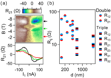
In order to help identify the electron-electron interactions responsible for frictional drag in this system, we have created several devices with differing and , as delineated in Table S\@slowromancapi@ and S\@slowromancapii@ in Supplemental Material Supplement . The maximum values for for the magnetic field range explored (0.2 T9 T) are plotted as a function of nanowire separation (Fig. 2(b)). Circle and square markers represent double-wire and triple-wire devices, respectively. Square markers are composed of red, blue and black segments that represent the arrangement of drive, drag and grounded wires, respectively. For example, a circle marker with blue on top corresponds to a measurement of in double wire device and a square one with color blue, black and red from top to bottom corresponds to a measurement for a triple-wire device. As shown in Fig. 2(b), the electron-electron interactions between the drive and drag nanowires exhibit large variations, with little if any explicit dependence on the nanowire separation . This unusual scaling with distance is a significant departure from the expected behavior if the Coulomb interaction were responsible for the drag resistance. In the case when a Coulomb interaction gives rise to a drag voltage in coupled nanowires, Raichev et al Raichev2000 predict that , where (10nm)-1 is the Fermi wave vector, and with being the dielectric constant of STO Muller1979 . Such an exponential decay with distance is absent in our measurements. Moreover, the exceptionally large dielectric constant of STO should lead to a suppression of by several orders of magnitude smaller compared with those measured in similar devices formed from other material systems Debray2001 ; Tokura2006 ; Laroche2014 ; however, no such reduction is found. The weak scaling with separation, and the insensitivity to the large dielectric constant of STO indicate that the electron-electron interactions responsible for frictional drag are non-Coulombic in nature.
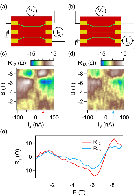
In order to further explore the nature of the long-range interactions leading to frictional drag, experiments with three parallel nanowires are investigated in detail. Schematics for two configurations (Figs. 3(a, b)) yield measurements of and , respectively (Figs. 3(c,d)), as a function of drive current and magnetic field. A comparison of and allows for the nanowire separation to be varied within a single device, and simultaneously probes the impact of introducing a central, grounded screening wire (for the case of ). Both the pattern as well as the magnitude of and are nearly identical, despite doubling (Fig. 3(e)). This result is consistent with the statistical findings summarized in Fig. 2(b). The frictional drag for the geometry is naively expected to be impacted by screening from the central wire. Instead, there is no discernable screening effect. The three-nanowire device geometry also enables one to ascribe the origin of the unique magnetic signature of the drag signal (i.e., Fig. 3(c) and 2 (a)) to properties of the drag wire and not the source wire.
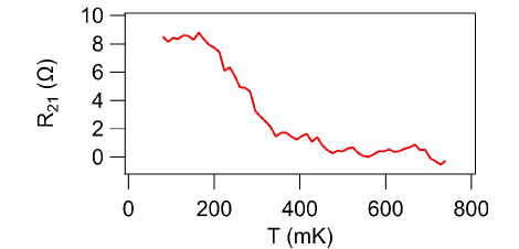
In 2D semiconductor drag systems, virtual phonon exchange was shown to be independent of distance Gramila1993 ; Tso1992 ; Tso1994 . The phonon-mediated coupling of the drag and drive systems, however, had a characteristice temperature scaling: the phonon mediated drag is expected to increase with increasing temperature Gramila1993 ; Narozhny2016 . Fig. 4 shows the typical temperature dependence of frictional drag. The drag resistance decreases monotonically with increasing temperature, becoming negligible for mK. This temperature dependence is inconsistent with phonon-mediated frictional drag reported for 2D systems.
Frictional drag measurements between nanowires created on the LAO/STO heterointerface exhibit a strong, distance-insensitive coupling which indicate a non-Coulombic interaction. The temperature dependence of this effect is incompatible with other known non-Coulombic interactions, such as virtual phonon exchange Gramila1993 ; Tso1992 ; Tso1994 ; Narozhny2016 . While these measurements do not specifically point to a particular coupling mechanism, there are candidates worth considering. STO possesses a bulk cubic structure at room temperature that is unstable to an antiferroeistortive transition to a tetragonal phase below 105 K Sakudo1971 . The ferroelastic domain structure gives rise to domain walls, which are correlated with anisotropic electronic phenomena observed at LAO/STO heterointerface Kalisky2013 . Ferroelastic domain walls are nominally insulating in the bulk, but they are also reported to be polar and mobile under applied electric fields. The coupling of ferroelastic strain states and local surface potentials Honig2013 could potentially mediate long-range interactions through the insulating near-surface bulk STO layer. Long-range couplings, whether mediated through ferroelastic domains or some other as-yet-unidentified mechanism, introduce a fascinating new element to the celebrated electronic properties of this oxide interface.
References
- (1) A. Ohtomo and H. Y. Hwang, Nature 427, 423 (2004).
- (2) N. Reyren, S. Thiel, A. Caviglia, L. F. Kourkoutis, G. Hammerl, C. Richter, C. Schneider, T. Kopp, A.-S. Retschi, D. Jaccard, M. Gabay, D. A. Muller, J.-M. Triscone, and J. Mannhart, Science 317, 1196 (2007).
- (3) A. Caviglia, S. Gariglio, N. Reyren, D. Jaccard, T. Schneider, M. Gabay, S. Thiel, G. Hammerl, J. Mannhart, and J.-M. Triscone, Nature 456, 624 (2008).
- (4) A. Brinkman, M. Huijben, M. Van Zalk, J. Huijben, U.Zeitler, J. Maan, W. G. van der Wiel, G. Rijnders, D. H. Blank and H. Hilgenkamp, Nature Materials 6, 493 (2007).
- (5) Y.-Y. Pai, A. Tylan-Tyler, P. Irvin, and J. Levy, arXiv:1610.0789.
- (6) M. Ben Shalom, M. Sachs, D. Rakhmilevitch, A. Palevski, and Y. Dagan, Phys. Rev. Lett. 104, 126802 (2010).
- (7) A. D. Caviglia, M. Gabay, S. Gariglio, N. Reyren, C. Cancellieri, and J.-M. Triscone, Phys. Rev. Lett. 104, 126803 (2010).
- (8) G. Cheng, M. Tomczyk, S. Lu, J. P. Veazey, M. Huang, P. Irvin, S. Ryu, H. Lee, C.-B. Eom, C. S. Hellberg, and J. Levy, Nature 521, 196 (2015).
- (9) G. Cheng, M. Tomczyk, A. B. Tacla, H. Lee, S. Lu, J. P. Veazey, M. Huang, P. Irvin, S. Ryu, C.-B. Eom, A. Daley, D. Pekker, and J. Levy, Phys. Rev. X 6, 041042 (2016).
- (10) S. Thiel, G. Hammerl, A. Schmehl, C. W. Schneider, and J. Mannhart, Science 313, 1942 (2006).
- (11) C. Cen, S. Thiel, G. Hammerl, C. W. Schneider, K. E. Andersen, C. S. Hellberg, J. Mannhart, and J. Levy, Nature Mater. 7, 298 (2008).
- (12) C. Cen, S. Thiel, J. Mannhart, and J. Levy, Science 323, 1026 (2009).
- (13) J. A. Sulpizio, S. Ilani, P. Irvin, and J. Levy, Annual Review of Materials Research 44, 117 (2014).
- (14) B. N. Narozhny and A. Levchenko, Rev. Mod. Phys. 88, 025003 (2016).
- (15) M. B. Pogrebinskii, Fiz. Tekh. Poluprovodn. 11, 637 [Sov. Phys. Semicond. 11, 372 (1977)].
- (16) P. M. Solomon, P. J. Price, D. J. Frank, and D. C. L. Tulipe, Phys. Rev. Lett. 63, 2508 (1989).
- (17) P. M. Solomon, and B. Laikhtman, Superlattices Microstruct. 10, 89 (1991).
- (18) T. J. Gramila, J. P. Eisenstein, A. H. MacDonald, L. N. Pfeiffer, and K. W. West, Phys. Rev. Lett. 66, 1216 (1991).
- (19) T. J Gramila., J. P. Eisenstein, A. H. MacDonald, L. N. Pfeiffer, and K. W. West, Surf. Sci. 263, 446 (1992).
- (20) T. J. Gramila, J. P. Eisenstein, A. H. MacDonald, L. N. Pfeiffer, and K. W. West, Physica (Amsterdam) 197B, 442 (1994).
- (21) J. P. Eisenstein, Superlattices Microstruct. 12, 107 (1992).
- (22) J. I. A. Li, T. Taniguchi, K. Watanabe, J. Hone, A. Levchenko, and C. R. Dean, Phys. Rev. Lett. 117, 046802 (2016).
- (23) K. Lee, J. Xue, D. C. Dillen, K. Watanabe, T. Taniguchi, and E. Tutuc, Phys. Rev. Lett. 117, 046803 (2016).
- (24) P. Debray, V. Zverev, O. Raichev, R. Klesse, P. Vasilopoulos, and R. S. Newrock, J. of Phys.: Cond. Matt. 13, 3389 (2001).
- (25) M. Yamamoto, M. Stopa, Y. Tokura, Y. Hirayama, and S. Tarucha, Science, 313, 204 (2006).
- (26) D. Laroche, G. Gervais, M. P. Lilly, and J. L. Reno, Science, 343, 631, (2014).
- (27) A. J. Keller, J. S. Lim, D. Sáchez, R. López, S. Amasha, J. A. Katine, H. Shtrikman, and D. Goldhaber-Gordon, Phys. Rev. Lett. 117, 066602 (2016).
- (28) T. J. Gramila, J. P. Eisenstein, A. H. MacDonald, L. N. Pfeiffer, and K. W. West, Phys. Rev. B 47, 12957 (1993).
- (29) H. C. Tso, P. Vasilopoulos, and F. M. Peeters, Phys. Rev. Lett. 68, 2516 (1992).
- (30) H. C. Tso,P. Vasilopoulos, and F. M.Peeters, Surf. Sci. 305, 400 (1994).
- (31) K. Brown, S. He, D. J. Eichelsdoerfer, M. Huang, I. Levy, H. Lee, S. Ryu, P. Irvin, J. Mendez-Arroyo, C.-B. Eom, C. A. Mirkin, and J. Levy, Nature Comm. , 10681 (2016).
- (32) F. Bi, D. F. Bogorin, C. Cen, C. W. Bark, J.-W. Park, C.-B. Eom, and J.Levy, Appl. Phys. Lett. , 173110 (2010).
- (33) A. Levchenko and A. Kamenev, Phys. Rev. Lett. 101, 216806 (2008).
- (34) See Supplemental Material at [URL will be inserted by publisher] for parameters of double- and triple-wire devices
- (35) O. E. Raichev and P. Vailopoulos, Phys. Rev. B 61, 7511 (2000).
- (36) K. A. Müller and H. Burkard, Phys. Rev. B 19, 3593 (1979).
- (37) T. Sakudo and H. Unoki, Physical Review Letters 26, 851 (1971).
- (38) B. Kalisky, E. M. Spanton, H. Noad, J. R. Kirtley, K. C. Nowack, C. Bell, H. K. Sato, M. Hosoda, Y. Xie, Y. Hikita, et al, Nat. Mat. 12, 1091 (2013).
- (39) M. Honig, J. A. Sulpizio, J. Drori, A. Joshua, E. Zeldov, and S. Ilani, Nat. Mat. 12, 1112 (2013).
Supplemental Material
In the supplemental document, two tables are provided that list device parameters for double-wire and triple-wire devices. Parameters for double-wire devices include lengths and separations between nanowires, two-terminal, four-terminal resistances of each wire and drag resistances measured from each wire. In the table for triple-wire devices, each row corresponds to a different measurement configuration depending on which two nanowires are used for drive and drag wires. For example 3 corresponds to the configuration where wire 1 and 2 are utilized and wire 3 is the grounded wire. is the drag resistance measured from wire 1 with wire 2 being the drive wire and vice-versa for . Due to the limitation of the number of electrodes there is no four-terminal resistance in triple-wire device table.
| Device | (nm) | (nm) | (k) | (k) | (k) | (k) | () | () |
|---|---|---|---|---|---|---|---|---|
| 2A | 400 | 40 | 58-72 | 42-48 | 31.3-43.5 | 8.4-9.2 | 20 | 60 |
| 2B | 400 | 40 | 22-31 | 26-34 | 8.6-12.5 | 14.0-18.3 | 14 | 4 |
| 2C | 1000 | 300 | 37-47 | 25-46 | NA | 8.7-18.4 | 51 | 23 |
| 2D | 1000 | 450 | 40-108 | 29-34 | NA | 6.4-7.5 | NA | 39 |
| 2E | 1500 | 550 | 27-35 | 29-63 | NA | 7.8-11.8 | 15 | 52 |
| 2F | 1500 | 550 | 22-29 | 33-77 | NA | NA | 27 | 26 |
| 2G | 1500 | 550 | 23-36 | 22-51 | 11.5-16.0 | 3.7-5.5 | 19 | 41 |
| 2H | 1500 | 1500 | 17-27 | 22-37 | 10.2-14.8 | 2.7-4.1 | 10 | 9 |
| 2I | 400 | 200 | 50-127 | 27-37 | 29.7-97.8 | 5.2-6.7 | NA | 76 |
| Config () | (nm) | (nm) | (k) | (k) | () | () |
|---|---|---|---|---|---|---|
| 3 | 1500 | 750 | 26-41 | 26-34 | 14 | 5 |
| 3 | 1500 | 1500 | 26-41 | 29-47 | 10 | 18 |
| 3 | 1500 | 750 | 26-34 | 29-47 | 8 | 30 |