Defect-enhanced Rashba spin-polarized currents in carbon nanotubes
Abstract
The production of spin-polarized currents in pristine carbon nanotubes with Rashba spin-orbit interaction has been shown to be very sensitive to the symmetry of the tubes and the geometry of the setup. Here we analyze the role of defects on the spin quantum conductances of metallic carbon nanotubes due to an external electric field. We show that localized defects, such as adsorbed hydrogen atoms or pentagon-heptagon pairs, increase the Rashba spin-polarized current. Moreover, this enhancement takes place for energies closer to the Fermi energy as compared to the response of pristine tubes. Such increment can be even larger when several equally spaced defects are introduced into the system. We explore different arrangements of defects, showing that for certain geometries there are flips of the spin-polarized current and even transport suppression. Our results indicate that spin valve devices at the nanoscale may be achieved via defect engineering in carbon nanotubes.
pacs:
73.63.-b, 72.25-bI Introduction
The departure from ideal crystalline order in carbon materials with hybridization, due to the presence of topological defects, lattice distortions and atomic adsorption have strong consequences in the physical properties of such nanosystems Padilha et al. (2011). In particular, these defects can create magnetic moments, as it has been observed in graphene by means of spin currents McCreary et al. (2012) or scanning tunneling microscopes (STM) Ugeda et al. (2010). Novel control and manipulation features of these microscopes Ugeda et al. (2010); González-Herrero et al. (2016) and advances in material growth techniques Sanchez-Valencia et al. (2014); Ruffieux et al. (2016) are the basis of outstanding experimental results. For instance, in a recent experiment the position of hydrogen adatoms in graphene has been modified with an STM, obtaining configurations in which all atoms were in a specific sublattice González-Herrero et al. (2016). Topological defects in graphene have been also created by electron beam focusing, achieving different structural defects by tuning the exposure time Robertson et al. (2012). Another experimental goal that is being recently attained is the ability to choose the particular geometry of nanoscale carbon materials. Typical examples are the chirality and radius of carbon nanotubes (CNTs) Sanchez-Valencia et al. (2014), or the width and edge shape of graphene nanoribbons Ruffieux et al. (2016).
Spin-polarized currents created by the applied electric field that induce a Rashba spin-orbit (RSO) interaction in carbon materials have been recently predicted Chico et al. (2015); Santos et al. (2016), even in the absence of external magnetic fields or magnetic impurities. These results indicate the possibility of producing stable spin-polarized electrical currents from unpolarized charge currents, paving the way toward the creation of carbon-based spin valve devices at the nanoscale. Such studies focused on ideal pristine carbon nanotubes and nanoribbons, for which the spin-polarized currents appear far from the Fermi energy (). However, the role of defects in carbon materials under a RSO interaction has not yet been addressed; defects might produce spin polarization of the conductance at energies around .
Vacancies, adsorption of hydrogen atoms, and defects in general act as localized perturbations in graphene systems and can induce localized states close to the Dirac point. The effects of such perturbations on the electronic properties of the system are greatly dependent on their position in the two sublattices of graphene and carbon nanotubes Lieb (1989); Saremi (2007); Palacios et al. (2008); Santos et al. (2014). When a orbital is removed from one sublattice of pristine graphene, due for instance to the creation of a vacancy, a new state appears on the other sublattice, localized around the perturbation Liang and Sofo (2012). Hydrogen adatoms also produce such localization effects; indeed, if we are not interested in the analysis of the resulting magnetic moments, we may consider both situations as equivalent.
The aim of the present work is to investigate how CNTs with defects may produce spin-polarized currents due to RSO coupling, thus possibly opening up novel routes for engineering the spin-dependent transport response on CNTs. We explore the possibility of enhancing such spin-polarized currents in CNTs closer to by introducing topological defects or hydrogen adatoms (H-adatoms) in the region with Rashba coupling. We focus on the effects of the particular positions of such defects, i.e., their spatial distribution and their relative orientation with respect to the electric field.
In principle, spin scattering is an important issue that may hinder the polarization of the current. Fortunately, the spin relaxation length in carbon systems is rather large; for example, the experimental value reported for carbon nanotubes is around 50 m Hueso et al. (2007). Therefore, as long as the size of the device or system studied is much smaller than this length, spin coherence should be maintained and spin polarization could be achieved. This is certainly plausible in nanoscale devices.
The article is organized as follows: In Sec. II we describe the systems, model and methods employed to obtain the spin transport properties under a RSO interaction. Section III deals with the effects of isolated adatoms and topological defects on the transport properties, the enhancement of spin-polarized currents due to multiple defects and the polarized-current dependence on their relative orientation; finally, the interplay of RSO interaction and the effects of random H-adatoms are explored. Finally, in Sec. IV we summarize our main results.
II System and model
II.1 Description of the system
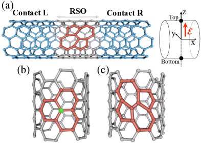
To analyze the effects of localized defects on the spin-polarized currents generated by the Rashba spin-orbit interaction (SOI), we propose a device made of a CNT that has a region of length placed between two metallic plates with an uniform electric field between them [see Fig. 1(a)]. As we are interested in transport properties, we concentrate on metallic nanotubes, and restrict the study to armchair tubes. The central part under the applied electric field has an induced Rashba spin-orbit (RSO) interaction; we name it the Rashba region. Notice that the system may be described as an infinite carbon nanotube with three parts: a central finite Rashba region connected to two semi-infinite nanotube leads of the same chirality and radius Santos et al. (2016). The length of the Rashba region can be given in terms of the length of the translational vector by (with Saito et al. (1992). Recall that for armchair tubes, where is the carbon bond length in graphene.
We introduce defects in this Rashba region. Specifically, as depicted in Fig. 1, we have chosen H-adatoms, shown in Fig. 1(b), and 5-7-7-5 Stone-Wales (SW) defects (i. e., two carbon pentagon-heptagon pairs placed antiparallel to each other), rendered in Fig. 1(c). The carbon atoms in which the defects produce important changes in the density of states are highlighted in red, being 12 atoms for the H-adatom and 16 for the SW defect.
The presence of H-adatoms does not mix the two CNT sublattices, although depending on their number and position, they may break the sublattice symmetry, allowing the appearance of localized magnetic moments on the atoms close to them Palacios et al. (2008). On the contrary, the introduction of topological defects in the hexagonal lattice of graphene or CNTs with an odd number of carbon atom rings mixes the two sublattices. Additionally, the combination of the two most probable topological defects in a carbon nanotube, a single 5-7 (pentagon-heptagon) pair, changes its chirality Chico et al. (1996); Charlier et al. (1996). However, two adjacent 5-7 pairs in opposite direction, the 5-7-7-5 SW defect, preserves the chirality of the CNT, but there is still a local sublattice mixing. With the aim to simplify the analysis, we focus only on defects that preserve the chirality, and so we study the effects of the RSO interaction on CNTs with H-adatoms and SW defects.
II.2 Model and method
Our calculation employs a single-orbital tight-binding model in the nearest-neighbor approximation with a RSO coupling limited to the central part of the carbon system Qiao et al. (2010); Lenz et al. (2013); Chico et al. (2015); Santos et al. (2016). The Hamiltonian can be written as , with the kinetic energy term being , where () is the creation (destruction) operator for electrons with spin projection in site (), and is the nearest-neighbor hopping energy, which is constant throughout the system. This amounts to neglecting the lattice relaxation produced by the defects, but this is a quantitative change with respect to lattice imbalance and mixing or orbital removal.
The RSO contribution to the Hamiltonian is
| (1) |
where are the Pauli spin matrices, is the position vector between sites and , and are the spin projection indices. The unit vector is along the electric field direction. The Rashba spin-orbit strength is given by the electric field intensity, and its sign defined by the field orientation. A value of is used Chico et al. (2015); Santos et al. (2016). Although this value is very large with respect to the intrinsic spin-orbit interaction of a pristine carbon nanotube, the enhancements reported for functionalized and decorated graphene systems Marchenko et al. (2012); Balakrishnan et al. (2014) suggest that similar values may be achieved in carbon nanotubes with defects.
As previously discussed Santos et al. (2016), the direction for which the spin-polarized current is largest is that perpendicular to both the current and the external electric field; in our case it corresponds to the direction. This fact can be best understood by resorting to the expression of the Rashba term in the continuum approximation R.Winkler (2003), i. e, , with being the wave vector which is in the direction of the current.
The conductance along the nanotube axis ( direction) is calculated following the Landauer approach in the zero bias approximation Chico et al. (1996); Santos et al. (2016). Assuming unpolarized charge currents flowing from left to right, the spin-dependent conductance is proportional to the probability that an electron with spin and energy in the left contact reaches right contact with spin . This probability can be calculated using the Green function formalism Xu et al. (2007); Diniz et al. (2012). The spin polarization of the conductance in the -direction is defined as
| (2) |
As already mentioned, we restrict ourselves to the direction for the spin projections. In the small-bias limit, this magnitude is proportional to the -component of the spin current. Although other authors employ a normalized adimensional spin polarization Zhai and Xu (2005); Diniz et al. (2012), we have chosen this definition which is directly related to the spin-dependent conductances .
The calculations are performed at zero temperature. We have checked that the effect of the temperature reduces and gives rise to a smoother dependence with the energy, as expected, but the differences between the spin-polarized currents are still significant at room temperature. As an indicative value, we have found a maximum decrease of the polarization peaks of 60 %. Such reduction does not preclude the possible measurement of the spin-polarized current and therefore, our results hold at room temperature.
III Results
We consider an infinite metallic armchair CNT with a central finite Rashba region of varying length , which is given in terms of the length of the translational vector, . We consider Rashba regions with a varying density of defects, and we also investigate the optimal condition for the relative orientation between the defects and the direction of the electric field. The Rashba interaction is switched on abruptly; we have verified that differences caused by considering a smooth profile for the electric field are irrelevant in the energy range of interest. Likewise, we have checked that the position of the defects within the Rashba region, i.e., with respect to its boundaries, is also unimportant in the energy range for which the bands are linear, around .
We assume that an unpolarized current flows from the left semiinfinite nanotube through the Rashba region towards the right lead. In Ref. Santos et al. (2016) we have shown that, for a pristine CNT, spin scattering in the Rashba region generates spin-polarized currents for certain spin directions and system symmetries. Here we analyze the effect of localized defects on the spin-polarized currents traversing the Rashba region.
As mentioned, we have focused on the analysis of the spin-projected conductance along the direction () perpendicular to both the current () and the external electric field () directions, since it exhibits the largest spin-polarized current. In particular, we get zero spin polarizations and for all the armchair nanotubes with an even index for symmetry reasons Santos et al. (2016). In contrast, the spin polarization of the conductance is maximized in the direction, for which there are no symmetry restrictions for its occurrence.
III.1 Single defects
The spin polarization of the conductances are evaluated for different sizes of the Rashba region, considering first the case of a single defect on the top position. Recall that we took the electric field direction to be , and the direction along the nanotube axis. We orient the nanotube so that the H-adatom is situated on the axis and the flux of the electric field through the area enclosed by the red highlighted bonds in Fig. 1(b) is maximum. For the SW defect, we proceed likewise, taking the axis passing through the middle point of the bond between the two adjacent heptagons in Fig. 1(c). Note that both, the top and bottom positions, give the maximal flux of the electric field (in absolute value) through these defects.
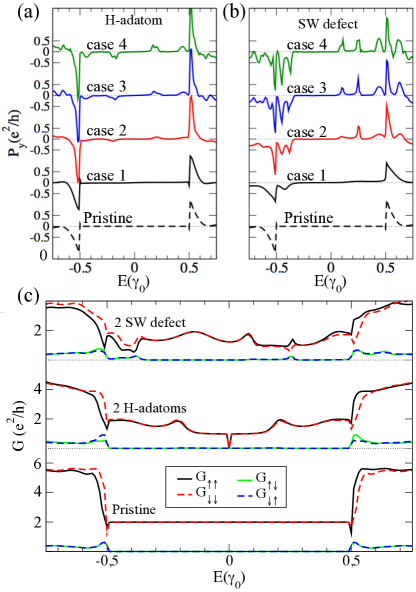
Figures 2(a) and 2(b) present for the pristine case and for the single defect case (case 1), using a Rashba region length nm, both for the H-adatom and the SW defect. Notice that for the pristine nanotube, the spin polarization of the conductance is zero for energies close to the Fermi level, even though there are two channels available for the conductance related to the two different valleys Zhai and Xu (2005). This is due to the lack of scattering processes in the Rashba region between states in different K valleys when the sole perturbation is the electric field Paul L. McEuen et al. (2016); Santos et al. (2016). But for energies close to , presents two peaks, allowed by the opening of other conductance channels in the nanotube contacts Santos et al. (2016). However, when a single defect (H-adatom or SW defect) is added to the Rashba region, intervalley scattering is allowed. But the effect, as shown in Figs. 2 (a) and (b), is too small to be noticeable for energies close to the Fermi level. These results for single defects are almost indistinguishable for the case of the H-adatom, whereas for the SW defect we observe small differences around peaks at [see case 1 in Figs. 2(a) and 2(b)]. Thus, when only one scattering center is considered in the Rashba region, the RSO effect close to the Fermi level is not easily distinguishable from the pristine case.
III.2 Multiple defects
In contrast to the single defect case, when we consider several equidistant defects at the top position of the Rashba region, the spin polarization of the conductance becomes significant close to the Fermi level. Previous works have analyzed the role of multiple defects in CNTs and graphene without taking RSO into account. Due to the symmetry of the honeycomb lattice, there are certain distances between scattering centers that produce an unusual scattering behavior at zero energy García-Lastra et al. (2008); Khalfoun et al. (2014); Santos et al. (2014): This happens if the defects in graphene or the unrolled nanotube sheet are placed at a distance such that , with , where are the graphene lattice vectors forming an angle of . Such distances are associated with wave vectors that couple the two Dirac points K and K’ at zero energy. But due to the linearity of the bands, intervalley coupling can be expected at other energies, provided that the bands are still linear. We choose different Rashba regions composed of finite CNT portions, each of them with a length and with a H-adatom or a SW defect in it. The defect density is kept constant, i.e., one defect per length . The top panels of Fig. 2 [(a) and (b)] show the spin polarization of the conductance for the cases . The heights of the maxima with energies within the first conductance plateau range of the pristine CNT increase with the number of defects. As for the defects are located at a distance verifying the condition of the coupling of the two Dirac cones, the enhancement of the spin-conserved conductances is very strong.
Such resonant behavior can be understood with a simple model for coherent scattering S.Datta (1997). Let be the transmission probability through a single impurity. The transmission through two identical scatterers is given by , where is the reflection probability by the single defect and is the phase shift acquired in one round trip between the scatterers. At the resonance () the total transmission is always 1, independently of the value of . In general, close to the resonance the transmission through the two defects is larger than , so the presence of a second impurity at a distance fulfilling a resonant condition always yields an enhancement of the conductance.
The bottom panel, Fig. 2 (c), represents the spin-dependent conductances as a function of the energy for the original pristine tube and the case . The presence of the two defects, either H-adatoms or SW defects, is evident for the spin-dependent conductances and near , being negligible for the spin-flip conductances and .
For the nanotube with two H-adatoms at a distance , exhibits small peaks at energies . The peaks coincide with the enhancement of the spin-dependent conductances from to due to the electronic states localized around the adatoms Santos et al. (2016). This effect is more remarkable as the number of equispaced adatoms in the Rashba region increases, as shown in Fig. 2 (a) (cases 3 and 4). We have explained this increase as a consequence of resonant scattering. Small differences in the wavevectors for spin up and down transmission yield a non-zero .
More relevant changes in the spin-polarized currents appear for the SW defects, as also shown in Fig. 2 (b). For case 2, two defects separated by , exhibits peaks at energies and ; these peaks are higher for larger number of defects (cases 3 and 4). On the other hand, for energies around (i.e., close to the transition from the first to the second conductance plateau of the pristine CNT leads) the for the SW defects exhibits many more features than for the H-adatoms. Due to sublattice mixing, the electron-hole symmetry is broken for the tubes with SW defects, yielding a strong asymmetry in the results. On the contrary, for the nanotube with H-adatoms shows electron-hole symmetry, .
Band structure and spin analysis
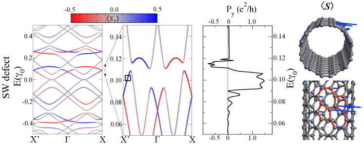
To understand the effect of H-adatoms and the SW defects in the spin-polarized currents induced by the Rashba SOI, we resort to the analysis of the spin-resolved band structure and the spin polarization of the conductance of an infinite periodic system. We choose a CNT unit cell of length with a single H-adatom or one SW defect in it, with the RSO interaction present in the whole system.
Figure 3(a) depicts the band structures for the CNT with Rashba SOI, with either H-adatoms (upper panel) or SW defects (bottom panel). The expectation values for the component of the spin, , projected in all the atoms around the defect or belonging to it (highlighted in red in Fig. 1), are shown with a color scale in the bands. The expectation value of the spin in the direction at a specific atom is given by , with , where is the tight-binding atomic eigenfunction in the single-orbital model. We have also plotted in Fig. 3 a zoom of the band structure in the relevant energy range [Fig. 3(b)] as well as the corresponding spin polarizations of the conductances [in Fig. 3(c)].
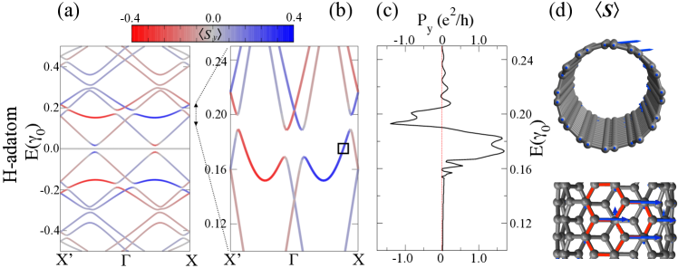
The bands of the periodic (6,6) CNT of length with one H-adatom present large absolute values of in the energy ranges from to , coinciding with the bumps of in Fig. 2(a) (with up to , where nm). These peaks in are much clearer in Fig. 3(c), obtained for a system with . Recall that for current flowing from left to right, the states that contribute to the current scattering process are those with positive velocity S.Datta (1997); Santos et al. (2009). The zoom in the top panel of Fig. 3(b) shows a band with a strong positive from to in the wavevector interval to . However, there is no band with negative in the same energy range, due to the opening of the gap around by the strong hybridization. At the same energy range shows a positive peak (Fig. 3(c), top). Besides, shows a negative peak from to , because the band with positive slope in that energy interval has negative .
The same analysis can be performed for CNTs with topological defects. The spin-resolved band structure for a periodic (6,6) nanotube with a SW defect is presented in the bottom panel of Fig. 3 (a). Large absolute values of occur from to and from to . As in the H-adatom case, the spin-polarized current appears when there is an inequality between the number of channels with opposite values of due to the gap opening. These energy ranges coincide with the enhancements shown in Fig. 2(b).
From these results we can assume that the states producing a spin polarization of the conductance are associated with the defects. To verify this assumption, we plot in Figs. 3 (d) the expectation values of the spin corresponding to the states which give rise to the polarized current at the atoms around (H-adatom) or composing (SW) the defect. Their wavevectors are marked with black squares in the zooms of the band structures presented in Figs. 3 (b). This expectation value is projected on each atom , , where , , , , and . Their energies and wavevectors are and for the H-adatom and and for the SW defect. The large absolute values of in those bands are located at the defects; thus, they are related to the high spin polarization of the conductances presented in Fig. 3 (c).
Taking into account the features of the bands shown for the periodic CNT with defects (Fig. 3), we conclude that the peaks of around are actually associated with the existence of equispaced defects in the Rashba region. It is important to note that besides the spin polarization of the bands, gaps should open at the same energies for other wavevectors. In this way, an imbalance between the channels with opposite values of the spin projection is produced, giving rise to spin-polarized currents.
It is noteworthy that if the distance between nearest defects does not fulfill the resonant condition (), after four or more repetitions an increase of the spin polarization of the current is produced anyway. Obviously, for , there are two impurities at a distance that verifies such condition, so the effect is always reinforced for periodically located defects. To illustrate this point, we present in Figs. 4 and 5 the cases of 20 equispaced H-adatoms and SW defects, respectively, on the top positions (A) with , showing quite strong peaks at similar energy ranges.
III.3 Influence of the relative alignment of defects and the electric field
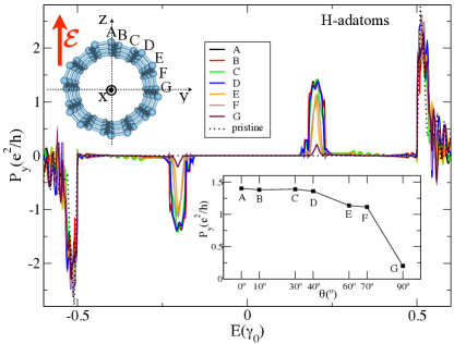
Here we analyze the dependence of the spin-polarized currents on the relative position of the defect in the original tube with respect to the direction of the electric field. We consider a (6,6) CNT with a Rashba region composed of with their corresponding adatoms equally spaced with , representing a sample with higher density of defects within the Rashba area. With the electric field along the axis, the relative orientation of the defects is varied from the parallel direction with respect to the field (top position, labeled A in Figs. 4 and 5) to the perpendicular direction (lateral side, labeled G), through intermediate positions. In Fig. 4 we present the results of the spin polarization of the conductance for the H-adatom, considering the positions in the tube shown in the inset of the figure. The peaks of close to the Fermi energy decrease in intensity as the H-adatom positions change from A to G, with a sharp reduction of from F to G. This is highlighted in the inset of Fig. 4, which shows the dependence of the maximum value of on the angle between the electric field and the normal to the defects. Such variation can be expected from the expression of the Rashba Hamiltonian: at position A, the vectors spanning the bonds in the defects are perpendicular to , maximizing their contribution to the Rashba term, whereas for position G the electric field is contained in the plane formed by these bonds, yielding a much smaller contribution. As mentioned, the electric flux of through the defects is maximal when the defects are at the top or the bottom positions on the nanotube. Therefore, the effect of the RSO is maximized for a maximum flux of the electric field through the defects.
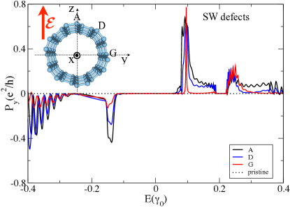
Similar results are found for the SW defects. Figure 5 shows for three relative orientation of the defects in the tube with respect to the electric field direction, indicated in the inset of the figure (positions A, D and G). The same defect density and length of the Rashba region employed for the H-adatoms are used here for the SW defects. Going from A to G, two noticeable effects can be observed. First, we see a large decrease of the peak at . In fact, the height of this peak when the defects are located at G (the lateral side of the tube) is only about of the value obtained for the top position A. Second, we observe a pronounced narrowing of the width of the peak that appears in the energy range between and . As expected, the relative position of the defects with respect to the electric field plays an important role in the spin polarization of the conductance.
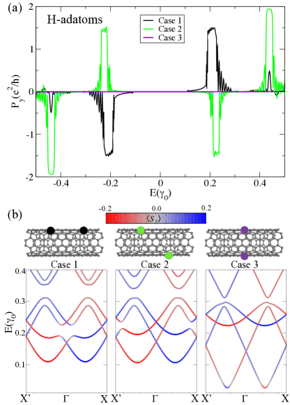
To investigate the effects of the relative positions of the defects, we further consider the case of two H-adatoms in the unit length , taking a Rashba region length equal to , where is . In case 1, two H-adatoms are both placed at the top of the tube. In case 2, one H-adatom is at the top and the other at the bottom of the tube, but not in diametrically opposite sites of the tube. In case 3 the H-adatoms are also at the top and the bottom of the tube, but exactly at opposite sites, in a symmetric configuration. The corresponding are shown in Fig. 6 (a). Again, for all cases we obtain two maxima of close to energies . It is noteworthy that changes depending on the relative position of the H-adatoms in the unit slab . For case 2 the peaks of are narrower than those of case 1, and their signs are reversed. For the symmetric case 3, the polarization completely disappears in the region corresponding to the first conductance plateau, identical to the results obtained for the pristine case.
To gain some insight into the main different features related to the relative position of the adatoms, we also resort to the band structures of infinite (6,6) CNTs with the same defect distributions showing the spin expectation value of the states in the bands, depicted in Fig. 6 (b). They present dramatic differences. The bands of case 1 show large anticrossings at around the energies , thus leaving unbalanced conduction channels with positive near X and X’. Case 2 shows the opposite behavior: the anticrossings take place near the X and X’ points, so the remaining channels close to have a negative spin projection . As a result, in case 2 the peaks of have inverted signs compared to case 1. In the symmetric case 3, polarizations and slopes of the bands are completely compensated. Since there are not any anticrossings nor band openings at these energies, the spin polarization of the conductances is zero, despite the fact that the bands show net spin expectation values.
These results can be of practical interest. The fact that adatoms situated on the same side of the tube give rise to spin-polarized currents that present inverted polarization signals when the H-adatoms are situated in opposite sides (top and bottom sides of the tube), may be of great importance, for instance, for transport and storage of spin information. Actually, DNA molecules wrapped around single-walled carbon nanotubes are shown to induce a helicoidal electric field due to the polar nature of the adsorbed DNA molecule Diniz et al. (2012) and spin-polarized currents are produced depending on the symmetry of the DNA molecule-nanotube hybrid system. Our results show that it could be possible to engineer particular defect configurations on the CNTs, opening new routes for their use in spintronic devices Alam and Pramanik (2015).
III.4 Irregularly spaced H-adatoms
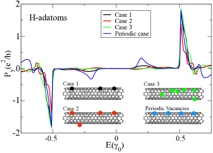
Finally, to extend our analysis beyond periodic configurations of defects, we have also considered several unequally spaced H-adatom distributions within the Rashba region (see the insets in Fig. 7). In cases 1 and 2 we have three and four H-adatoms in top and bottom positions with different spacings. Seven adatoms at random positions have been used in case 3. Four equispaced H-adatoms have also been calculated for comparison. In all cases, the length of the Rashba region is taken as nm.
Figure 7 shows for these different adatom distributions. For cases 1 to 3 the height of those peaks closer to the Fermi energy is clearly smaller than for the equispaced defects. Therefore, it appears that the best scenario to obtain spin-polarized conductances in these CNTs is when the H-adatoms are in a periodic arrangement within the Rashba region.
IV Summary
We have presented a detailed study of the effects of H-adatom and Stone-Wales defects on the spin-polarized currents induced by a RSO interaction in metallic carbon nanotubes. Our main results show that (i) defects produce an increase of the spin-polarized currents at energies close to the Fermi energy; (ii) spin-polarized currents appear when an imbalance between the number of spin-polarized conductance channels with opposite spin direction takes place at the same energy, and furthermore (iii) such currents are greatly enhanced when the defects are periodically introduced in the system. Actually, a single defect scenario is insufficient to generate significant spin-dependent currents, but adding a few equispaced defects yields significant results. In summary, introducing a regular array of defects in the Rashba region is optimal for the obtention of spin-polarized currents in carbon materials. This can be explained as a consequence of resonant tunneling through the multiple defects.
We have also found the importance of the orientation of the defects with respect to the direction of the electric field that causes the RSO interaction. Specifically, we have observed that a change in the relative position of neighbor defects (from top-top to top-bottom) produces a reversal of the spin polarization , which can be exploited as a spin switch. Our results can be useful for exploring new routes in the design of spintronic devices with CNTs.
V Acknowledgments
A. L. acknowledges the financial support of FAPERJ through Grants No. E-26/102.272/2013 and No. E-26/202.953/2016, CNPq, and INCT em Nanomateriais de Carbono. L. C. acknowledges support from Spanish MINECO through Grant No. FIS2015-64654-P, and helpful conversations with Jorge I. Cerdá. H. S. is grateful for financial support from the Brazilian CAPES.
References
- Padilha et al. (2011) J. Padilha, R. Amorim, A. Rocha, A. da Silva, and A. Fazzio, Solid State Communications 151, 482 (2011).
- McCreary et al. (2012) K. M. McCreary, A. G. Swartz, W. Han, J. Fabian, and R. K. Kawakami, Phys. Rev. Lett. 109, 186604 (2012).
- Ugeda et al. (2010) M. M. Ugeda, I. Brihuega, F. Guinea, and J. M. Gómez-Rodríguez, Phys. Rev. Lett. 104, 096804 (2010).
- González-Herrero et al. (2016) H. González-Herrero, J. M. Gómez-Rodríguez, P. Mallet, M. Moaied, J. J. Palacios, C. Salgado, M. M. Ugeda, J.-Y. Veuillen, F. Yndurain, and I. Brihuega, Science 352, 437 (2016).
- Sanchez-Valencia et al. (2014) J. R. Sanchez-Valencia, T. Dienel, O. Groning, I. Shorubalko, A. Mueller, M. Jansen, K. Amsharov, P. Ruffieux, and R. Fasel, Nature 512, 61 (2014).
- Ruffieux et al. (2016) P. Ruffieux, S. Wang, B. Yang, C. Sánchez-Sánchez, J. Liu, T. Dienel, L. Talirz, P. Shinde, C. A. Pignedoli, D. Passerone, T. Dumslaff, X. Feng, K. Müllen, and R. Fasel, Nature 531, 489 (2016).
- Robertson et al. (2012) A. W. Robertson, C. S. Allen, Y. A. Wu, K. He, J. Olivier, J. Neethling, A. I. Kirkland, and J. H. Warner, Nature Comm. 3, 1144 (2012).
- Chico et al. (2015) L. Chico, A. Latgé, and L. Brey, Phys. Chem. Chem. Phys. 17, 16469 (2015).
- Santos et al. (2016) H. Santos, A. Latgé, J. E. Alvarellos, and L. Chico, Phys. Rev. B 93, 165424 (2016).
- Lieb (1989) E. H. Lieb, Phys. Rev. Lett. 62, 1201 (1989).
- Saremi (2007) S. Saremi, Phys. Rev. B 76, 184430 (2007).
- Palacios et al. (2008) J. J. Palacios, J. Fernández-Rossier, and L. Brey, Phys. Rev. B 77, 195428 (2008).
- Santos et al. (2014) H. Santos, D. Soriano, and J. J. Palacios, Phys. Rev. B 89, 195416 (2014).
- Liang and Sofo (2012) S.-Z. Liang and J. O. Sofo, Phys. Rev. Lett. 109, 256601 (2012).
- Hueso et al. (2007) L. Hueso, J. M. Pruneda, V. Ferrari, G. Burnell, J. P. Valdés-Herrera, B. D. Simmons, P. B. Littlewood, E. Artacho, A. Fert, and N. D. Mathur, Nature (London) 445, 410 (2007).
- Saito et al. (1992) R. Saito, M. Fujita, G. Dresselhaus, and M. Dresselhaus, Appl. Phys. Lett. 60, 2204 (1992).
- Chico et al. (1996) L. Chico, V. H. Crespi, L. X. Benedict, S. G. Louie, and M. L. Cohen, Phys. Rev. Lett. 76, 971 (1996).
- Charlier et al. (1996) J.-C. Charlier, T. W. Ebbesen, and P. Lambin, Phys. Rev. B 53, 11108 (1996).
- Qiao et al. (2010) Z. Qiao, S. Yang, W. Feng, W.-K. Tse, J. Ding, Y. Yao, J. Wang, and Q. Niu, Phys. Rev. B 82, 161414 (2010).
- Lenz et al. (2013) L. Lenz, D. F. Urban, and D. Bercioux, Eur. Phys. J. B 86, 502 (2013).
- Marchenko et al. (2012) D. Marchenko, A. Varykhalov, M. R. Scholz, G. Bihlmayer, E. I. Rashba, A. Rybkin, A. M. Shikin, and O. Rader, Nat. Commun. 3, 1232 (2012).
- Balakrishnan et al. (2014) J. Balakrishnan, G. K. W. Koon, A. Avsar, Y. Ho, J. H. Lee, M. Jaiswal, S.-J. Baeck, J.-H. Ahn, A. Ferreira, M. A. Cazalilla, A. H. Castro Neto, and B. Özyilmaz, Nat. Commun. 5, 4748 (2014).
- R.Winkler (2003) R.Winkler, Spin-Orbit Coupling Effects in Two-Dimensional Electron and Hole Systems (Springer-Verlag Berlin, 2003).
- Xu et al. (2007) F. Xu, B. Li, H. Pan, and J.-L. Zhu, Phys. Rev. B 75, 085431 (2007).
- Diniz et al. (2012) G. S. Diniz, A. Latgé, and S. E. Ulloa, Phys. Rev. Lett. 108, 126601 (2012).
- Zhai and Xu (2005) F. Zhai and H. Q. Xu, Phys. Rev. Lett. 94, 246601 (2005).
- Paul L. McEuen et al. (2016) P. L. Paul L. McEuen, D. H. Bockrath, Marc and. Cobden, Y.-G. Yoon, and S. G. Louie, Phys. Rev. Lett. 83, 5098 (2016).
- García-Lastra et al. (2008) J. M. García-Lastra, K. S. Thygesen, M. Strange, and A. Rubio, Phys. Rev. Lett. 101, 236806 (2008).
- Khalfoun et al. (2014) H. Khalfoun, P. Lambin, and L. Henrard, Phys. Rev. B 89, 045407 (2014).
- S.Datta (1997) S.Datta, Electronic Transport in Mesoscopic Systems (Cambridge University Press, 1997).
- Santos et al. (2009) H. Santos, L. Chico, and L. Brey, Phys. Rev. Lett. 103, 086801 (2009).
- Alam and Pramanik (2015) K. M. Alam and S. Pramanik, Adv. Funct. Mater. 25, 3210 (2015).