Mobility in excess of cm2/Vs in InAs quantum wells grown on lattice mismatched InP substrates
Abstract
InAs-based two-dimensional electron systems grown on lattice mismatched InP substrates offer a robust platform for the pursuit of topologically protected quantum computing. We investigated strained composite quantum wells of In0.75Ga0.25As/InAs/In0.75Ga0.25As with In0.75Al0.25As barriers. By optimizing the widths of the In0.75Ga0.25As layers, the In0.75Al0.25As barrier, and the InAs quantum well we demonstrate mobility in excess of cmVs. Mobility vs. density data indicates that scattering is dominated by a residual three dimensional distribution of charged impurities. We extract the Rashba parameter and spin-orbit length as important material parameters for investigations involving Majorana zero modes.
Due to a combination of strong spin-orbit coupling, large g-factor, and readily-induced proximity superconductivity the InAs based two-dimensional electron gas (2DEG) has gained traction recently as a promising platform for topological quantum computing (Sarma et al., 2005; Alicea et al., 2011; Shabani et al., 2016; Kjaergaard et al., 2016, 2017; Suominen et al., 2017; Nichele et al., 2017). A structure composed of a shallow InAs quantum well can be engineered to have proximity induced superconductivity with an in-situ epitaxial Al top layer with high transparency (Shabani et al., 2016). This system has been demonstrated to contain Andreev bound states that coalesce into Majorana zero modes (Suominen et al., 2017; Nichele et al., 2017). However, a pressing limitation is the quality of the 2DEG.
We investigate the limitations of 2DEG mobility in the InAs on InP substrate system. Low temperature transport measurements are performed on gated Hall bars using symmetric In0.75Ga0.25As/InAs/In0.75Ga0.25As quantum wells grown on (100) InP where we vary the width of the flanking InGaAs layers, the depth of the quantum well from the surface, and the width of the InAs layer. While InAs has a 3.3 lattice mismatch to InP, the superior insulating property of Fe-doped InP substrates presents a crucial advantage for the measurement of high impedance devices necessary for the exploration of Majorana physics. Our results demonstrate record charge carrier mobility in excess of cmVs for this system and that our mobility appears to be limited by unintentional background charge impurities. We extract the Rashba parameter and spin-orbit length from the beating pattern of Shubnikov de-Haas oscillations. These results may be leveraged to improve the quality of InAs 2DEG structures used for topological quantum computing.
| In0.75Al0.25As | In0.75Ga0.25As | InAs | |
|---|---|---|---|
| Sample A | nm | nm | nm |
| Sample B | nm | nm | nm |
| Sample C | nm | nm | nm |
| Sample D | nm | nm | nm |
| Sample E | nm | nm | nm |
Our samples are grown using molecular beam epitaxy (MBE); see Ref. (Gardner et al., 2016) for greater detail on how our MBE has been set up and maintained. The InAs structures are grown on semi-insulating InP (100) substrates that have been desorbed at C until a to surface phase transition is observed. First, a 100 nm thick In0.52Al0.48As lattice matched smoothing layer upon which a In0.52Al0.48As/In0.52Ga0.48As nm five period superlattice is grown at C (Heyn et al., 2003). Due to a native lattice mismatch of 3.3 between InAs and InP we grow a step graded buffer of InxAl1-xAs where to using 18, nm wide each, followed by a linearly ramped reverse step from to to relieve any residual strain. The graded buffer layer and reverse step are grown at C.
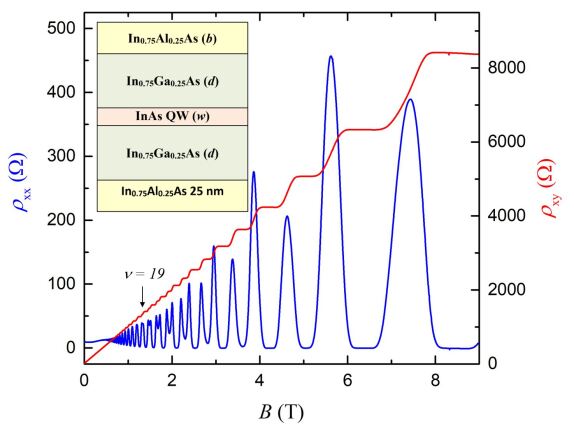
The active region comprised of the composite quantum well plus barriers is then grown. The substrate temperature is increased to C to grow a nm In0.75Al0.25As bottom barrier and active region composed of a strained nm (nm for Sample E only) InAs layer flanked on either side by symmetric In0.75Ga0.25As layers to promote higher mobility (Sexl et al., 1997; Wallart et al., 2005). For Samples A, B, and C, we vary only the width of the In0.75Ga0.25As layers to be and nm, respectively. The sample growth is completed with a nm (nm for Sample D only) In0.75Al0.25As top barrier to remove the active region from the surface and minimize anisotropy effects that can become apparent when the active region of the quantum well is to near the surface (Lohr et al., 2003). Lastly, we do not include an InGaAs capping layer to avoid formation of a parallel conduction channel (Shabani et al., 2014a) or intentional doping. In the inset of Fig. 1 we schematically depict the layer stack for the active region. A summary of the five samples discussed here are presented in Table 1.

Our samples are processed with standard wet etching techniques to define both straight and L-shaped (aligned along the and directions) Hall bars of width m. After etching we deposit Ti/Au ohmic contacts of thickness nm, a 40 nm Al2O3 dielectric using thermal atomic layer deposition, and a nm Ti/Au gate. All samples have a zero gate voltage, , density of cm-2 with versus in good agreement with a simple capacitance model. The samples were measured in a 3He system at a base temperature of mK using standard low frequency lockin techniques with excitation current of A.
InAs quantum wells based on GaSb substrates with Al0.37Ga0.67Sb barriers (Shojaei et al., 2016) have recently been shown to achieve mobilities of cmVs at cm-2(Tschirky et al., 2017). The sample structures investigated here are instead grown on lattice mismatched InP substrates that have superior insulating properties, a requirement when operating mesoscopic devices in high resistance configurations. To our knowledge, the highest reported mobility for such a structure is cmVs achieved at cm-2 (Shabani et al., 2014a), but supporting transport data was not provided.
We begin our discussion with Sample B, which yielded the highest mobility. In Fig. 1 we present longitudinal (, left axis) and Hall ( in units of inverse filling factor, right axis) resistivities versus magnetic field () for cm-2. We observe the absence of a parasitic parallel conduction channel from the linear low field . There is also good agreement between the extracted density from both the Hall slope and the period of Shubnikov de-Haas oscillations (SdHOs). With increasing we observe a spin splitting onset at filling factor , where is the Planck constant and the electron charge, as marked in Fig. 1, with well developed integer quantum Hall states, and , where is an integer.

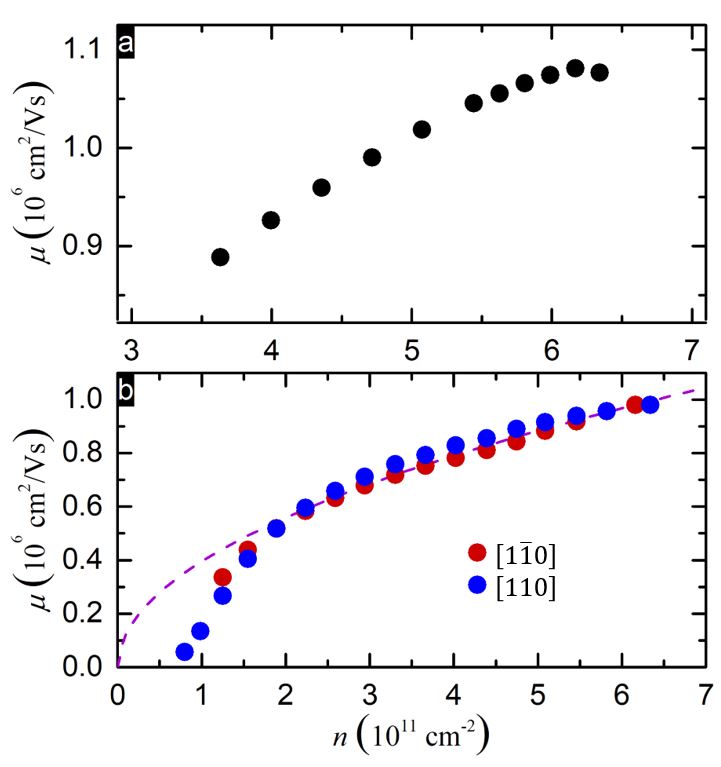
We continue with Sample B with gating to obtain versus , shown in Fig. 2 (a) for a straight Hall bar aligned along the direction. A maximum mobility of cmVs occurs at cm-2. To our knowledge this is the largest reported for an InGaAs/InAs/InGaAs quantum well. On a device processed during a different fabrication, from the same wafer as Sample B, we plot versus where measurements were performed on an L-shaped Hall bar in Fig. 2 (b). The gating dependence shows that there is minimal anisotropy between the and directions with less than difference. Thus we compare samples only along the direction for the remainder of the manuscript.
To determine what limits mobility in our structure we assume the vs dependence can be described by a simple power law, , and extract the exponent , using a log-log plot (not shown) giving equal weight to all data, in the restricted density range of cm-2. In Fig. 2 (b) the extracted fit, dashed line, for fits well over the density range of interest and is roughly equivalent for all samples measured in this study. In Ref. (Shabani et al., 2014b) a similar structure was investigated that contained nm In0.75Ga0.25As layers where it is was observed that . These -values indicate that the mobility is limited by unintentional background impurities (Sarma and Hwang, 2013). Theoretically, in the strong screening, where is the Thomas-Fermi wave vector (Stern, 1967), and high density limit , however, in the case of remote two-dimensional impurities . For comparison, Ref. (Shabani et al., 2014b) investigated a sample with an additional nm In0.75Ga0.25As capping layer and observed , where the increase in was attributed to an unintentional parallel surface channel. It is plausible that the introduction of this capping layer enhanced a remote layer that was competing with the background impurities favoring an increase in . The difference between and could also be due to unintentional background impurities within the well, as evidenced by the difference in over the same range (Sarma and Hwang, 2013). At present the exact nature of the charged impurities in our samples cannot be specified, but since a 2DEG is formed in the absence of modulation doping it is reasonable to assume that ionized donor-like defects exist in the lattice. Identification of the precise location and density of such defects requires further investigation beyond the scope of this paper.

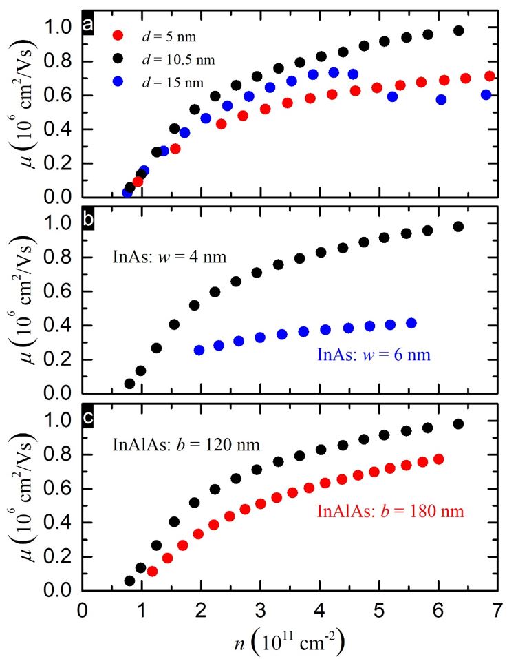
Comparison of the quality of our samples is evaluated using zero-field mobility as the metric. We next investigate perturbations to Sample B beginning with the well width dependence of the In0.75Ga0.25As layers. In Fig. 2 (c) we plot versus for Samples A-C where the In0.75Ga0.25As layer widths are and nm, respectively. For Sample C, nm, there is a nonmonotonic versus where begins to decrease for cm-2. This nonmonotonic -dependence is due to occupation of the second subband. Estimation of the onset density of the second subband becoming populated occurs at and cm-2 for Samples A-C, respectively, from self consistent calculations performed with Nextnano3 (nex, ).
At fixed there is a nonmonotonic dependence of versus . At cm-2, for example, cmVs for nm that decreases to cmVs and cmVs for and nm, respectively. With a large overlap in sample structure between the three samples we do not expect changes in scattering from background impurities, remote impurities, or charged dislocations due to the lattice mismatch to give reasonable explanation to the observed width dependence. Increasing results in a spread of the charge distribution such that there is an increase of the amount of charge that resides in the In0.75Ga0.25As layers. An increase of the amount of wavefunction extension into the In0.75Ga0.25As layer will decrease the mobility due to an increase in the amount of alloy scattering. The small decrease of of is due to a transfer of charge from the pure InAs to the In0.75Ga0.25As layer implies a strong dependence on alloy scattering. A more dramatic reduction in the mobility occurs when there is a decrease of , which can come from two sources 1) alloy scattering and 2) interface scattering. The charge distribution in the effective nm well of Sample C will penetrate into the In0.75Al0.25As barriers giving an increased amount of alloy scattering, as observed in Nextnano3 simulations. Additionally, the increased confinement of the charge results in an increase in scattering at the In0.75Ga0.25As/InAs interface. Comparison of the integrated charge density of the wells of Sample B and C in a restricted region of nm to either side of the InGaAs/InAs interface shows that the amount of charge in the region of the interface increases giving rise to increased interface scattering.
In Fig. 3 (b) versus for Sample B and D where the width of the InAs quantum well is increased from to nm is plotted. A large reduction in throughout the entire -range for nm is observed. Naively one might expect to increase with an increase in as a larger percentage of the charge density would reside in the InAs part of the well resulting in a decrease in alloy scattering from the In0.75Ga0.25As layers. However, the severe reduction in implies that the critical thickness, , of the InAs has been exceeded which introduce misfit dislocations to the quantum well (Capotondi et al., 2005; Shabani et al., 2014a). We estimate nm, for this In concentration.
In Fig. 3 (c) we plot versus for increase of the In0.75Al0.25As barrier from to nm, Samples B and E respectively. Again there is an overall decrease in . As previously discussed is limited by background charged impurities which suggests that while is increased in Sample E to reduce surface effects the possible gain is compensated by the increased level of charged impurities introduced by the additional In0.75Al0.25As layers resulting in decreased .

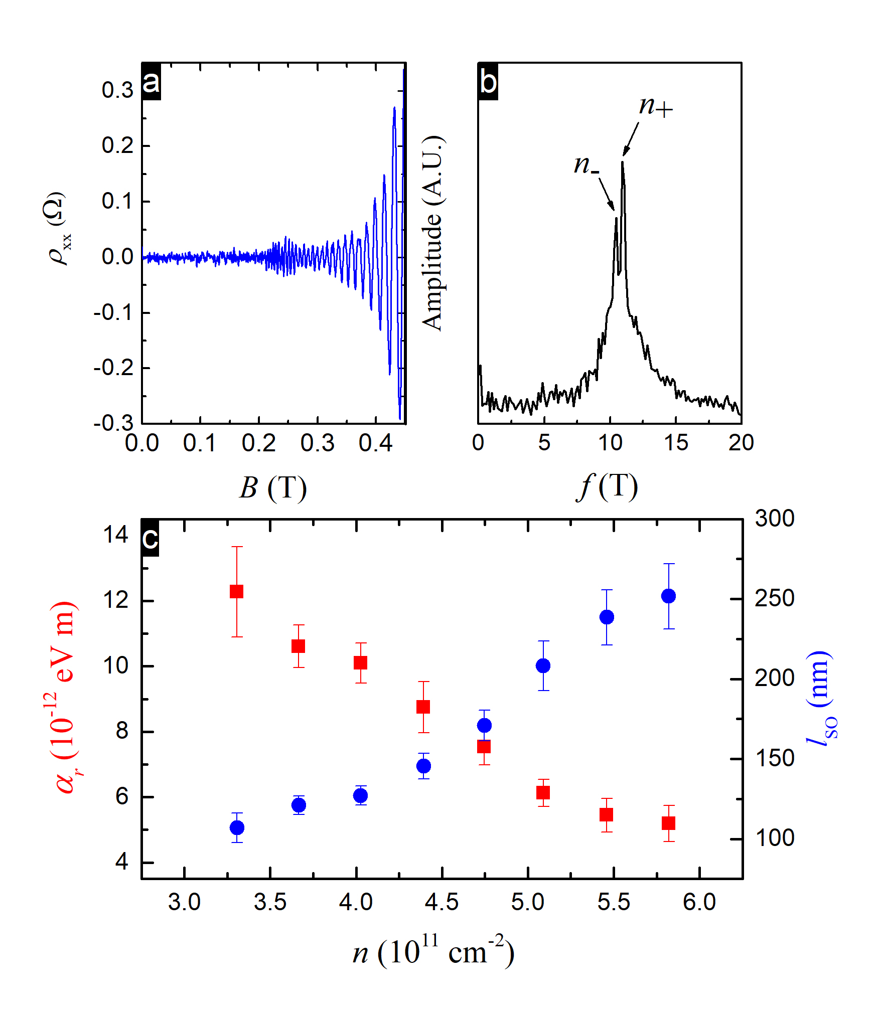
We preformed further measurements of Sample B at low to investigate the spin-orbit coupling. In Fig. 4 (a) we plot the oscillatory correction to the magnetoresistivity, , for cm-2 after removal of a slowly varying background. With increasing we observe the onset of SdHOs at T, this low value is another indication of the high quality of the 2DEG. The amplitude of the SdHOs increase with increasing but demonstrate a beating pattern with a node at T. By restricting our analysis to densities below occupation of the second subband, this beating pattern can be ascribed to two oscillation periods that are nearly equal and has been demonstrated in these structures to arise from zero field spin splitting between slightly different spin up and spin down densities (Datta and Das, 1990; Kim et al., 2010; Lee et al., 2011).
In Fig. 4 (b) we present the amplitude of the Fast Fourier Transform (FFT) versus frequency of the magnetotransport after conversion to inverse magnetic field. This FFT split peak can be assigned to two spin-split subbands with densities and , which can be calculated from . From this assignment, the estimated total density is in good agreement with that obtained from the Hall slope and the SdHO minima period.
In systems that lack inversion symmetry the dominant source of spin-orbit interaction is due to the Rashba effect, which arises from an electric field perpendicular to the plane of the 2DEG. This electric field can be a result of an inversion asymmetry built into the system based on 2DEG design or from an applied field from a gate (Nitta et al., 1997). From the SdHO beating pattern we extract the Rashba parameter , where and we assume (Shabani et al., 2014b). We perform FFTs at different and extract versus in Fig. 4 (c), left axis. The Rashba effect is due to an asymmetry in the azimuthal direction and is proportional to the electric field, where is a material specific parameter. Our gating density dependence is very nearly linear and follows from the simple capacitance model where we observe a linear change to so we expect a linear increase of with decreasing , corresponding to an increase in . The values we obtain for are of the same order as those obtained from InAs systems with symmetric Si doping (Kim et al., 2010), built in In0.53Ga0.47As layer asymmetry (Lee et al., 2011; Park et al., 2013), or those reported with AlSb barriers (Shojaei et al., 2016).
To eliminate effective mass dependence we recast as the spin-orbit length, , versus and plot the result in Fig. 4 (c), right axis. Physically, the spin-orbit length gives a measure of the average distance traversed by an electron before a spin flip occurs. In the case of weak spin-orbit interaction, the high (low ) case, the spin will travel further through the system, larger , before its spin orientation will become essentially randomized. With increase of the spin-orbit interaction under applied gate voltage the electron traverses decreasing distance before its spin is randomized.
This research supported by Microsoft Station Q.
References
- Sarma et al. (2005) S. D. Sarma, M. Freedman, and C. Nayak, Phys. Rev. Lett. 94, 166802 (2005).
- Alicea et al. (2011) J. Alicea, Y. Oreg, G. Refael, F. von Oppen, and M. P. A. Fisher, Nat. Phys. 7, 412 (2011).
- Shabani et al. (2016) J. Shabani, M. Kjaergaard, H. J. Suominen, Y. Kim, F. Nichele, K. Pakrouski, T. Stankevic, R. M. Lutchyn, P. Krogstrup, R. Feidenhans’l, et al., Phys. Rev. B 93, 155402 (2016).
- Kjaergaard et al. (2016) M. Kjaergaard, F. Nichele, H. J. Suominen, M. P. Nowak, M. Wimmer, A. R. Akhmerov, J. A. Folk, K. Flensberg, J. Shabani, C. J. Palmstrom, et al., Nat. Commun. 7, 12841 (2016).
- Kjaergaard et al. (2017) M. Kjaergaard, H. J. Suominen, M. P. Nowak, A. R. Akhmerov, J. Shabani, C. J. Palmstrom, F. Nichele, and C. M. Marcus, Phys. Rev. Applied 7, 034029 (2017).
- Suominen et al. (2017) H. J. Suominen, M. Kjaergaard, A. R. Hamilton, J. Shabani, C. J. Palmstrom, C. M. Marcus, and F. Nichele, Ariv e-prints p. arXiv:1703.03699 (2017).
- Nichele et al. (2017) F. Nichele, A. C. C. Drachmann, A. M. Whiticar, E. C. T. O’Farrell, H. J. Suominen, A. Fornieri, T. Wang, G. C. Gardner, C. Thomas, A. T. Hatke, et al., Ariv e-prints p. arXiv:1706.07033 (2017).
- Gardner et al. (2016) G. C. Gardner, S. Fallahi, J. D. Watson, and M. J. Manfra, Journal of Crystal Growth 441, 71 (2016).
- Heyn et al. (2003) C. Heyn, S. Mendach, S. Löhr, S. Beyer, S. Schnüll, and W. Hansen, Journal of Crystal Growth 251, 832 (2003).
- Sexl et al. (1997) M. Sexl, G. Bohm, D. Xu, H. Heib, S. Kraus, G. Trankle, and G. Weimann, Journal of Crystal Growth 175, 915 (1997).
- Wallart et al. (2005) X. Wallart, J. Lastennet, D. Vignaud, and F. Mollot, Applied Physics Letters 87, 043504 (2005).
- Lohr et al. (2003) S. Lohr, S. Mendach, T. Vonau, C. Heyn, and W. Hansen, Phys. Rev. B 67, 045309 (2003).
- Shabani et al. (2014a) J. Shabani, A. P. McFadden, B. Shojaei, and C. J. Palmstrom, Applied Physics Letters 105, 262105 (2014a).
- Shojaei et al. (2016) B. Shojaei, A. C. C. Drachmann, M. Pendharkar, D. J. Pennachio, M. P. Echlin, P. G. Callahan, S. Kraemer, T. M. Pollock, C. M. Marcus, and C. J. Palmstrom, Phys. Rev. B 94, 245306 (2016).
- Tschirky et al. (2017) T. Tschirky, S. Mueller, C. A. Lehner, S. Falt, T. Ihn, K. Ensslin, and W. Wegscheider, Phys. Rev. B 95, 115304 (2017).
- Shabani et al. (2014b) J. Shabani, S. D. Sarma, and C. J. Palmstrom, Phys. Rev. B 90, 161303 (2014b).
- Sarma and Hwang (2013) S. D. Sarma and E. H. Hwang, Phys. Rev. B 88, 035439 (2013).
- Stern (1967) F. Stern, Phys. Rev. Lett. 18, 546 (1967).
- (19) The Nextnano software can be obtained from http://www.wsi.tum.de/nextnano3 and http://www.nextnano.de.
- Capotondi et al. (2005) F. Capotondi, G. Biasiol, D. Ercolania, and L. Sorbaa, Journal of Crystal Growth 278, 538 (2005).
- Datta and Das (1990) S. Datta and B. Das, Appl. Phys. Lett. 56, 665 (1990).
- Kim et al. (2010) K.-H. Kim, H. Kim, H. C. Koo, J. Chang, and S.-H. Han, Applied Physics Letters 97, 012504 (2010).
- Lee et al. (2011) T. Y. Lee, J. Chang, M. C. Hickey, H. C. Koo, H.-J. K. S. H. Han, and J. S. Moodera, Applied Physics Letters 98, 202504 (2011).
- Nitta et al. (1997) J. Nitta, T. Akazaki, H. Takayanagi, and T. Enoki, Phys. Rev. Lett. 78, 1335 (1997).
- Park et al. (2013) Y. H. Park, H. jun Kim, J. Chang, S. H. Han, J. Eom, H.-J. Choi, , and H. C. Koo, Applied Physics Letters 103, 252407 (2013).