figurec
Towards visualisation of central-cell-effects in scanning-tunnelling-microscope images of subsurface dopant qubits in silicon
Abstract
Atomic-scale understanding of phosphorous donor wave functions underpins the design and optimisation of silicon based quantum devices. The accuracy of large-scale theoretical methods to compute donor wave functions is dependent on descriptions of central-cell-corrections, which are empirically fitted to match experimental binding energies, or other quantities associated with the global properties of the wave function. Direct approaches to understanding such effects in donor wave functions are of great interest. Here, we apply a comprehensive atomistic theoretical framework to compute scanning tunnelling microscopy (STM) images of subsurface donor wave functions with two central-cell-correction formalisms previously employed in the literature. The comparison between central-cell models based on real-space image features and the Fourier transform profiles indicate that the central-cell effects are visible in the simulated STM images up to ten monolayers below the silicon surface. Our study motivates a future experimental investigation of the central-cell effects via STM imaging technique with potential of fine tuning theoretical models, which could play a vital role in the design of donor-based quantum systems in scalable quantum computer architectures.
Nuclear or electron spin qubits based on dopant impurities in silicon are promising candidates for the implementation of quantum computing architectures Kane (1998); Hollenberg et al. (2006); Hill et al. (2015); Pica et al. (2016). The design and control of robust quantum logic gates demand atomic-scale fabrication Fuechsle et al. (2012); Weber et al. (2012) and understanding of the dopant wave functions Rahman et al. (2007); Usman et al. (2015a, b). The strength of dopant wave function at the nuclear site is proportional to the contact hyperfine interaction (A), and its long-range spatial distribution underpins the exchange-coupling (J) interaction between dopant pairs – A and J being two crucial control parameters in the design of quantum logic gates Hill et al. (2015); Kalra et al. (2014); Zwanenburg et al. (2013). Therefore an accurate description of the dopant wave function has been a long-standing fundamental physics problem Kohn and Luttinger (1955); Wilson and Feher (1961); Pantelides and Sah (1974); Martins et al. (2004); Friesen (2005), which has recently attracted renewed research interest Rahman et al. (2007); Pica et al. (2014a); Gamble et al. (2015); Wellard and Hollenberg (2005); Usman et al. (2015a, b); Salfi et al. (2014); Usman et al. (2016).
The atomistic description of donor wave function can exhibit central-cell-effects (CCEs) based on underpinning central-cell-corrections (CCCs) implemented in a particular theoretical model Usman et al. (2015a). These CCEs have been reported to affect the hyperfine Stark shift under the application of electric and strain fields Usman et al. (2015b) and the exchange interaction between two P atoms Pica et al. (2014b); Saraiva et al. (2015); Wellard and Hollenberg (2005). Currently, benchmarking theoretical descriptions of CCCs has been carried out with respect to measured values of the binding energies and hyperfine with and without electric fields and strain Usman et al. (2015a); Pica et al. (2014b); Saraiva et al. (2015); Wellard and Hollenberg (2005); Rahman et al. (2007). While such benchmarking of the hyperfine interaction have provided information about the CCCs at the nuclear site, the exchange interaction depends on the long-range spatial distribution of the wave functions, and hence requires investigation of CCEs over a large number of atoms around the P donors. In this work, we demonstrate that scanning tunnelling microscopy (STM) imaging of near surface donors Salfi et al. (2014); Usman et al. (2016) now provides a way towards much more detailed probing of the spatial distribution of donor wave functions. By theoretically computing STM images based on two different implementations of CCCs employed in the literature, we establish the potential of directly visualising CCEs by STM images, paving the way for high-precision benchmarking of donor states.
Atomistic approaches to calculating and understanding donor wave functions has a long history. The application of the first principle methods (DFT, ab-initio) Overhof and Gerstmann (2004); Smith et al. (2016) to the calculation of the dopant wave functions in silicon can capture physics at the donor site, however these approaches are limited to a small number of atoms in the simulation domain due to the requirement of intense computational resources and therefore cannot provide a long-range spatial description of the wave function required for the designing of multi-qubit gates. Momentum based approaches have been engineered to include central-cell and dielectric effects Wellard and Hollenberg (2005), providing a good description at intermediate scales. For realistic-sized devices with dimensions in the range of 30-50 nm, two commonly employed methods are based on continuum effective-mass Koiller et al. (2002); Pica et al. (2014a); Gamble et al. (2015); Pica et al. (2014b) and atomistic tight-binding Usman et al. (2016, 2015b); Ahmed et al. (2009); Rahman et al. (2007) theories, both relying on empirical fitting of the central-cell-corrections (CCCs) to the experimentally measured binding energies and degeneracies of the donor 1s states. This procedure of computing donor states has limited accuracy as it usually relies on benchmarking of the energies without taking into account the spatial distribution of the wave function itself. In this work we employ a comprehensive theoretical treatment of the entire STM-donor system in an atomistic tight-binding framework Usman et al. (2016) to investigate whether the impact of central-cell-corrections can be discerned in the context of recently reported STM imaging approach.
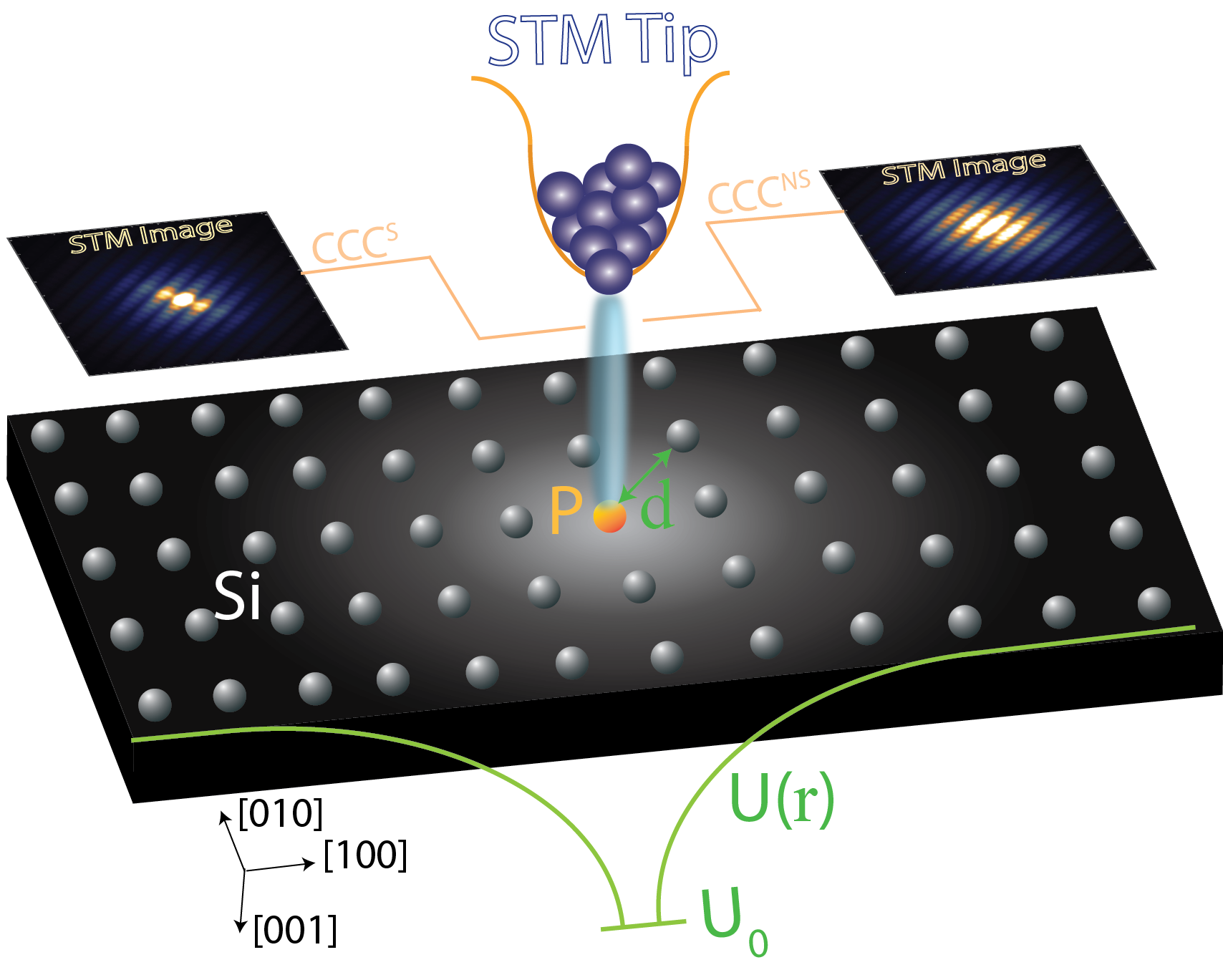
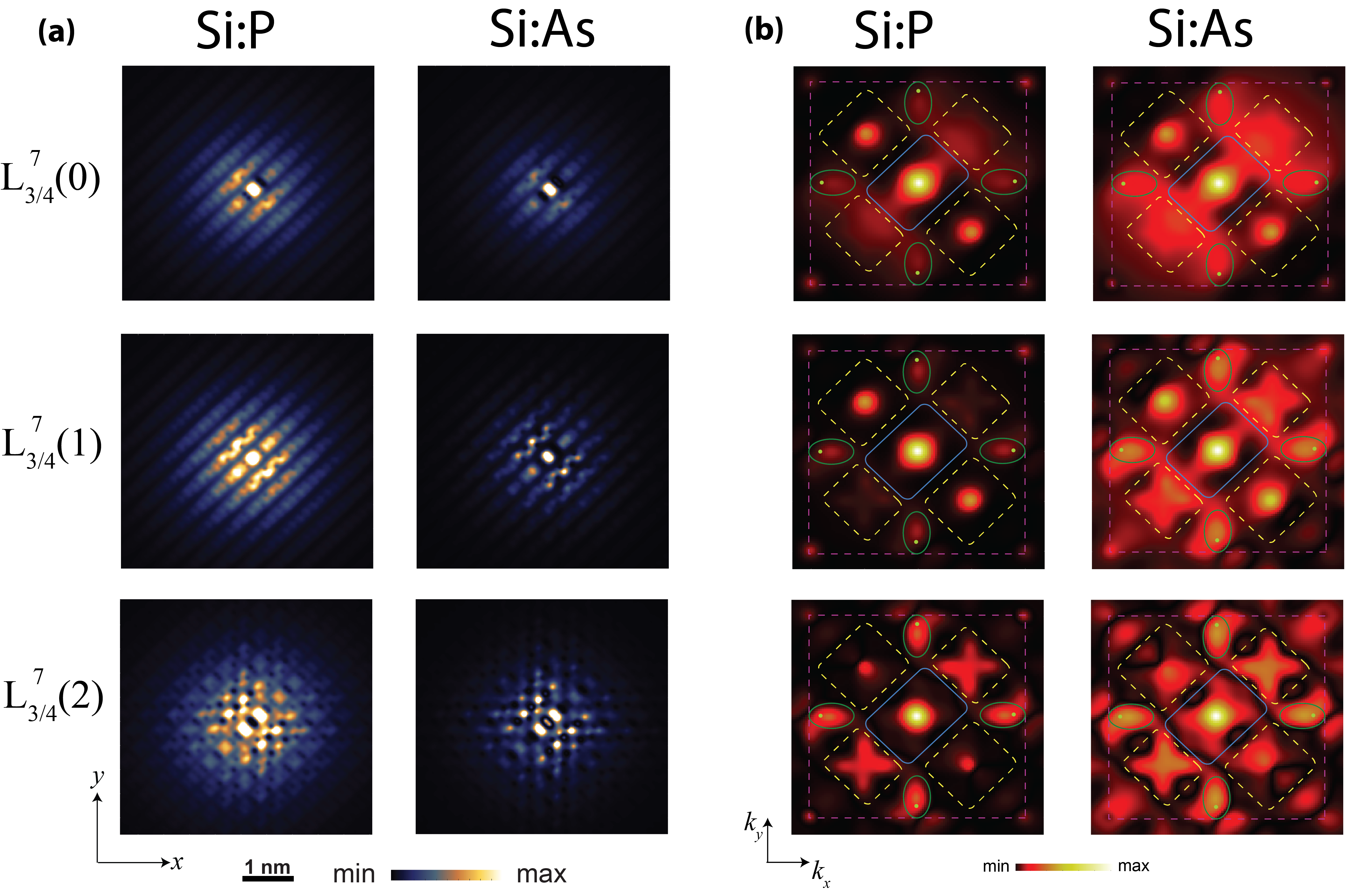
Figure 1 schematically illustrates the setup for STM imaging. We consider a P or As donor located a few monolayers (MLs) below the silicon surface. The wave function distribution of the donor is strongly dependent on central-cell-effects, which modify the donor potential (through a core-cutoff U0, or screening of the potential U() itself) and/or donor-Si bond-length (). STM images are computed from the donor wave functions and are directly related to the underpinning CCEs for up to 10 mono-layers below the hydrogen-passivated (001) silicon surface. As we will show later, a direct theoretical correlation can be established between the computed images and the corresponding donor wave functions. Furthermore, we note that phosphorous (P) and arsenic (As) donor wave functions are primarily different due to the central-cell-effects Usman et al. (2015b), with the CCC induced difference in wave functions being much stronger between the donor species, than between donors of the same species with different CCC implementations. Our results show that the computed STM images for P and As donor wave functions indeed exhibit this stronger effect.
Central-cell-corrections in tight-binding theory:
The implementation details of the central-cell-effects in theoretical models vary considerably in the literature. For instance, the screening of donor potential by silicon dielectric constant has been performed either by a static value Martins et al. (2004); Ahmed et al. (2009); Rahman et al. (2007); Pica et al. (2014b), or a non-static -dependent dielectric screening function Pantelides and Sah (1974); Wellard and Hollenberg (2005); Usman et al. (2015a, b). The bond-length deformation (intrinsic strain) around the donor atom has only been taken into account recently Overhof and Gerstmann (2004); Usman et al. (2015a). To investigate the visualization of the central-cell effects in the computed STM images, here we select the two most often used implementations of central-cell-corrections – static corrections (CCCS) and non-static corrections (CCCNS) (see the supplementary material section S1 for detailed descriptions). Briefly, the CCCS model is based on a minimal set of central-cell-corrections, where a Coulomb-like donor potential is cut-off at U0=-3.782 eV, which is selected to match the ground state binding energy of the donor atom Ahmed et al. (2009). The long-range tail of the potential is screened by a static value of dielectric constant for silicon (=11.7). The CCCNS model is much more detailed description Usman et al. (2015a), in which the long-range tail of the potential screened by a non-static dielectric function Nara (1965) given by:
| (1) |
where is 10.8, and the fitting parameters A, , , and are 1.175, 0.7572, 0.3223, and 2.044 in atomic units. The cut-off potential (U0) at the donor site is now adjusted to -3.5 eV to match the ground state binding energy. Additionally the nearest-neighbour Si-P bond-lengths are also strained by 1.9% Overhof and Gerstmann (2004). Both CCC models have been implemented within the atomistic tight-binding framework for the electronic structure calculations Usman et al. (2015a); Rahman et al. (2007); Klimeck et al. (2007a); Boykin et al. (2004). For the purpose of computing wave function images which are measured via low temperature STM scan Salfi et al. (2014), we have not taken free carrier screening into account. Since the P donor based spin qubit devices are typically operated at very low temperatures Fuechsle et al. (2012); Weber et al. (2012), free carrier screening is not important for the presented work. It should be noted that both implementations of CCCs reproduce the ground state binding energy of P atom with high accuracy (with in 1 eV of the experimentally measured value of 45.6 meV Ramdas and Rodriguez (1981)), however the spatial profiles of the wave functions exhibit clear differences due to the different strengths of donor potential screenings, which is being investigated in this work based on the simulated STM images. It is also important to note that the above model is a very realistic description of the STM experiment. Specifically, although the electric potential applied to the STM tip can in general introduce charges in the substrate, we have chosen the tip voltage to avoid charges during the measurement of the donor state Salfi et al. (2014). Conversely, in our experimental setup the tip potential can be chosen to apply an electric field to the quantum state, or even to induce a single-electron quantum dot beneath the tip Salfi et al. (2017).
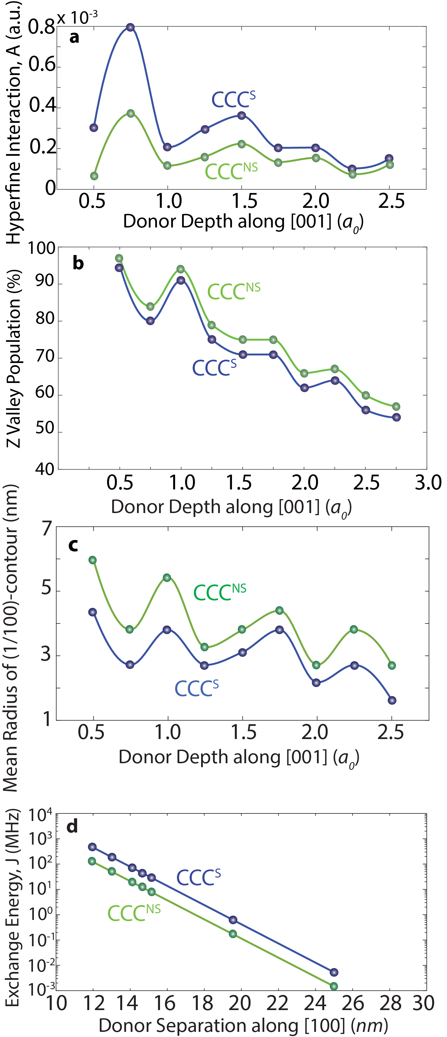
The important role of central-cell-corrections in the design of donor based quantum devices is evident from the past studies, where based on effective-mass theory Saraiva et al. (2015); Pica et al. (2014b) and band-minimum-basis approach Wellard and Hollenberg (2005), it has been shown that the strength of exchange interaction between two P atoms is highly dependent on the implementation of donor potential screening in the CCCs. The role of CCCs in the tight-binding theory has recently been shown to accurately reproduce the experimentally measured electric field and strain induced Stark shifts of the hyperfine frequency Usman et al. (2015a, b). Here the impact of the two implemented CCC models (CCCNS and CCCS) on the parameters of interest for the donor based quantum devices is provided in supplementary figure S1, which plots the peak amplitudes of wave function charge densities (which is proportional to the contact hyperfine interactions (A)), Z-valley populations, and the exchange-interaction energies () computed from the two CCC models. The differences between these parameters directly arise due to the atomistic details of the underlying donor wave functions, which considerably vary depending on the selected implementation of the CCC model. It should also be noted that the CCC induced variation in these quantities becomes further pronounced under the application of electric Wellard and Hollenberg (2005) and strain fields Usman et al. (2015b) typically employed for controlled operation of quantum devices.
Calculation of STM images:
The calculation of the STM images (tunnelling current) from the donor wave functions follows the recently reported methodology Usman et al. (2016) (see also details in supplementary section S2). First the vacuum decay of the donor state at the STM tip position is computed by using the Slater-orbital basis functions Slater (1930). The tunnelling current () is proportional to the magnitude square of the tunnelling matrix element in accordance with Bardeen’s tunnelling theory Bardeen (1961), whose exact relation with the vacuum-decayed wave function follows the nature of the STM tip orbital configuration as derived by Chen’s derivative rule Chen (90 I). To be consistent with the STM measurements reported earlier Usman et al. (2016), we assume the tunnelling current is dominated by orbital state in the STM tip and therefore can be calculated as:
| (2) |
where is the donor wave function and is the position of the STM tip.
Here we shall point out that although the orbital might be more localized than s or p type orbitals as discussed in some other work Blanco et al. (2006), our experimental measurements unambiguously confirm that the dominant orbital in the STM tunnelling current is orbital. This is attributed to the fact that the STM images of subsurface donor atoms in Si have very large spatial extent (overall size of an STM image is 8 nm 8 nm), and they exhibit a well-defined symmetry of lattice-sized bright features stemming from valley-related oscillations. We have investigated the role of different tip orbitals and found that the symmetry of the measured STM image features is only reproduced by orbital in the STM tip Usman et al. (2016). This is also consistent with some previous studies where orbital dominance was predicted for transition metal element tips Chen (90 I); Chaika et al. (2010); Teobaldi et al. (2012).
Visualisation of CCC effects in STM images:
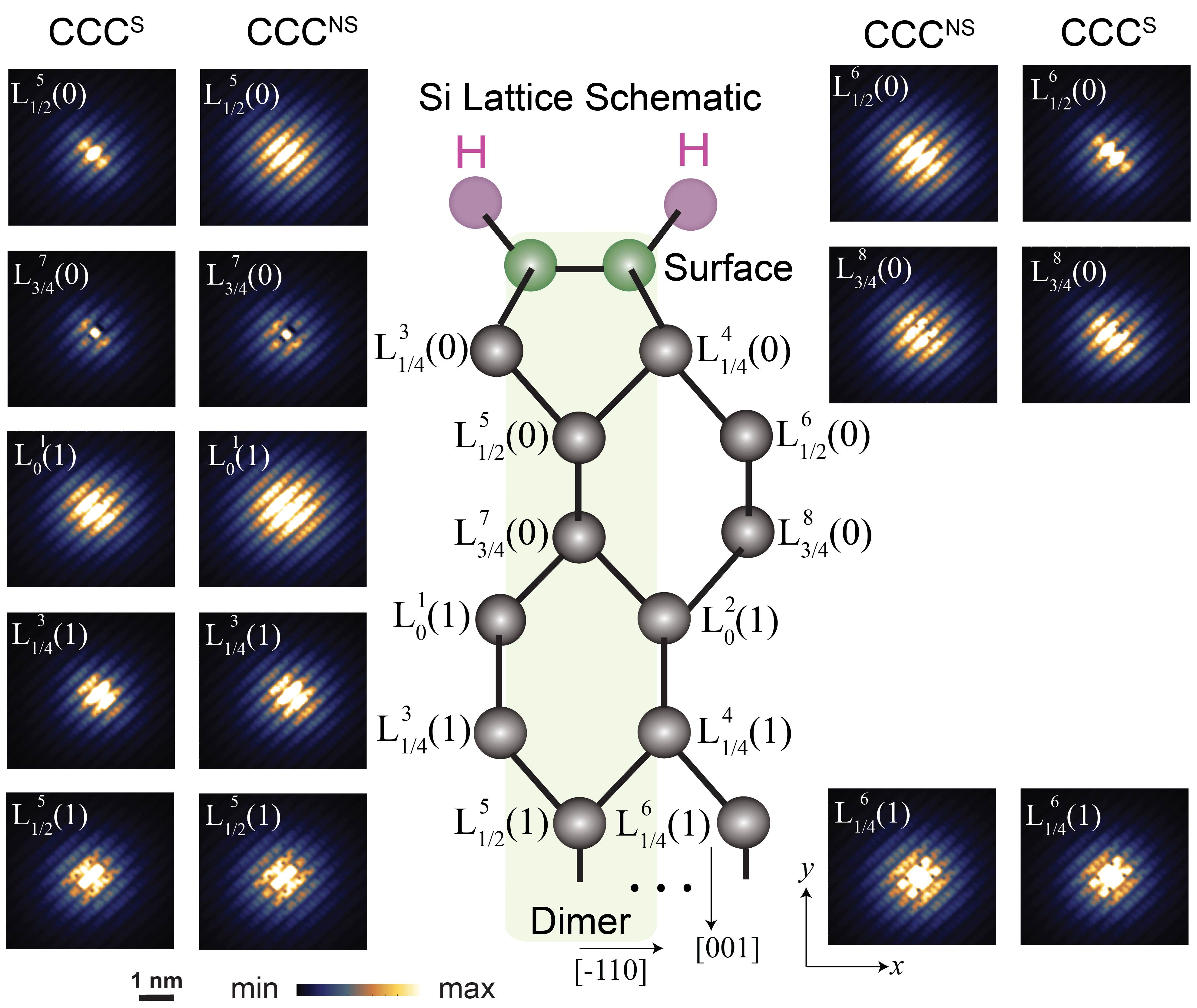
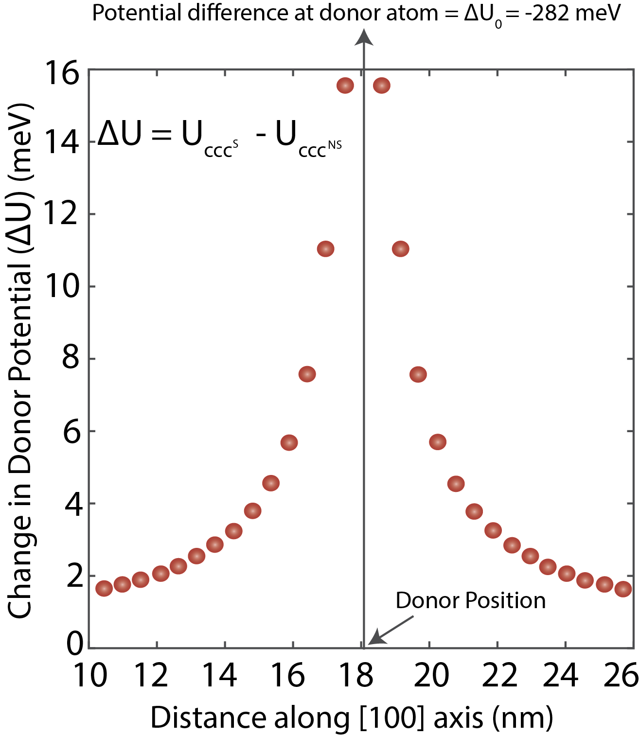
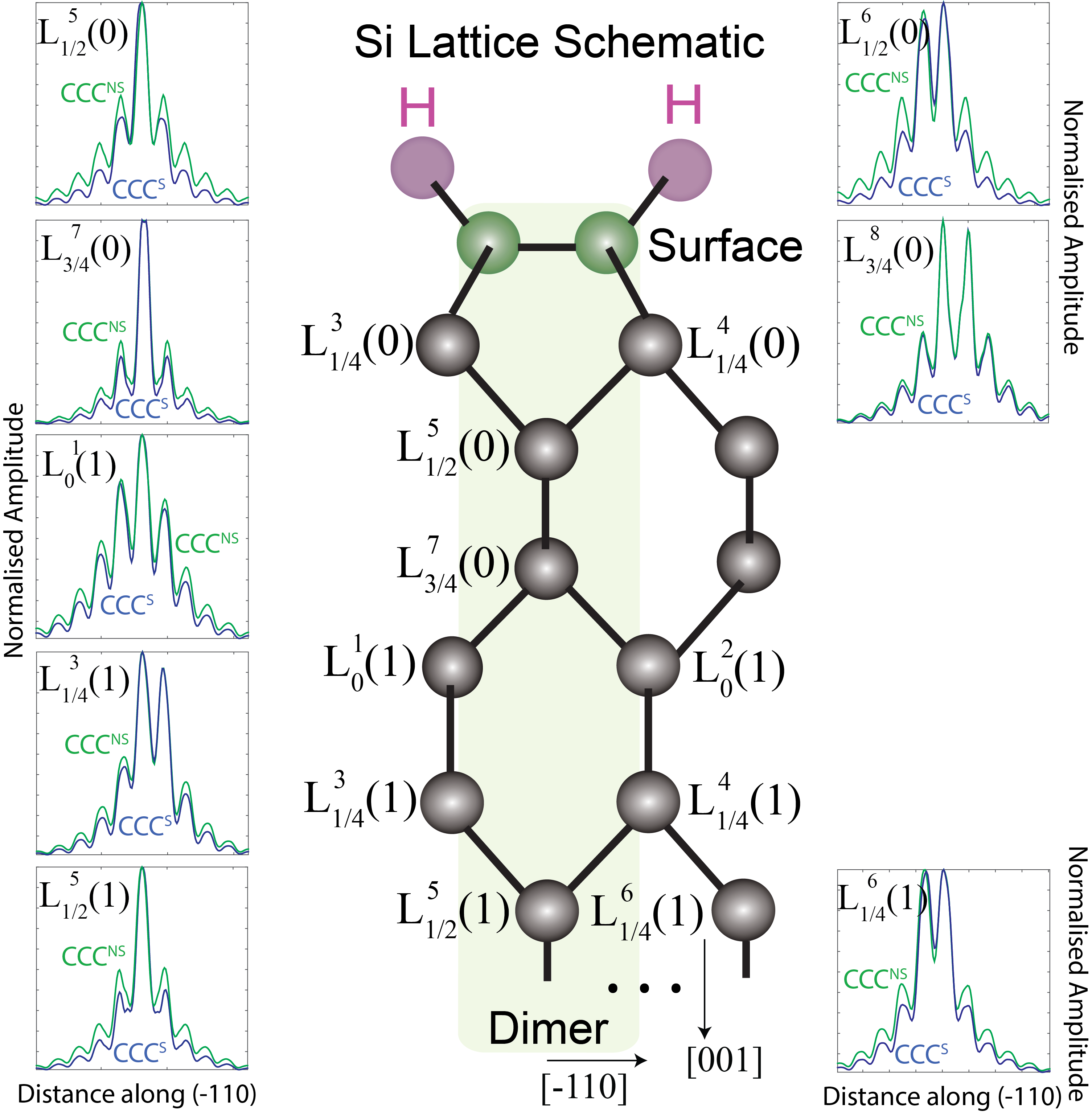
Figure S2 plots the real-space STM images computed with the two CCCS and CCCNS models for the available lattice positions within the first five unstrained monolayers below the hydrogen passivated silicon surface. The labelling of the atom positions follows the notation of our earlier work Usman et al. (2016), and has been briefly reiterated in the caption of the figure S2. In this study, we do not consider the STM images for the atom positions in the (m,n)=(1/4,0) plane, which is directly connected to the (m,n)=(0,0) surface atoms and therefore experience additional strain due to the formation of surface dimer rows (21 reconstruction). The images are normalised and plotted using the same color scale to enable a direct comparison. The images computed from the two CCC models exhibit visible differences, which can be quantified by their spatial extent and color intensity. Furthermore, the line cut profiles through the center of the images along the (-110) direction are also plotted in supplementary figure S2, which provide a quantitative comparison between the image features computed from the two CCC models. The size and the brightness of features in STM images are a measure of the spatial distribution of the underlying donor wave function, as the tunnelling current at any given tip position is directly related to the magnitude of the wave function charge density underneath it. The STM images computed from the CCCNS model consistently exhibit brighter features when compared to the CCCS model, thereby implying larger amplitudes of donor wave function density on the surrounding silicon atoms. In order to relate this effect with the CCC potential profile, we also plot in figure S3 the difference between the donor potentials implemented in the two CCC models. At the donor site, the difference between the two cut-off potentials is U0 is (-3.782) (-3.5) = -0.282 eV, indicating that the magnitude of the negative cut-off potential is significantly reduced for the CCCNS model. This leads to a reduction of the wave function density () at the donor site from 4.051030 m-3 for CCCS to 2.961030 m-3 for CCCNS model, resulting in a better agreement with the measured value Feher (1959) of 1.731030 m-3. The spatial profile of the donor wave function on the surrounding silicon atoms is modified by the long-range tail of the potential. Here a larger negative donor potential for the CCCNS model leads to an increase of the donor wave function density on the silicon atoms, resulting in brighter features in the STM images. Therefore, we conclude that for the donor positions in the top-most ten monolayers below the Si surface, the difference between STM images computed from the two CCC models provide a clear evidence of the underlying CCC effects on the corresponding donor wave functions.
Quantitative correlation between STM images and wave function parameters:
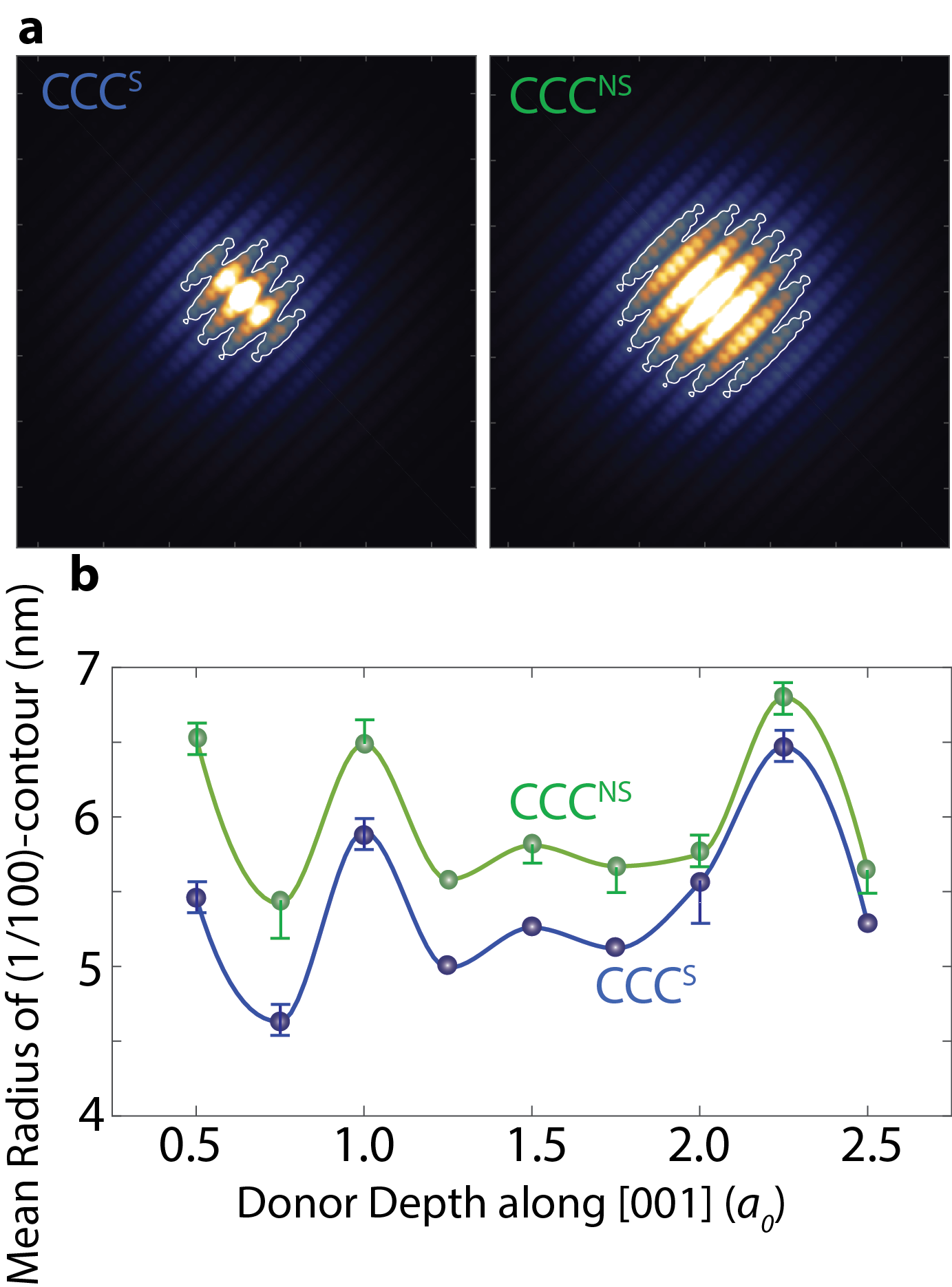
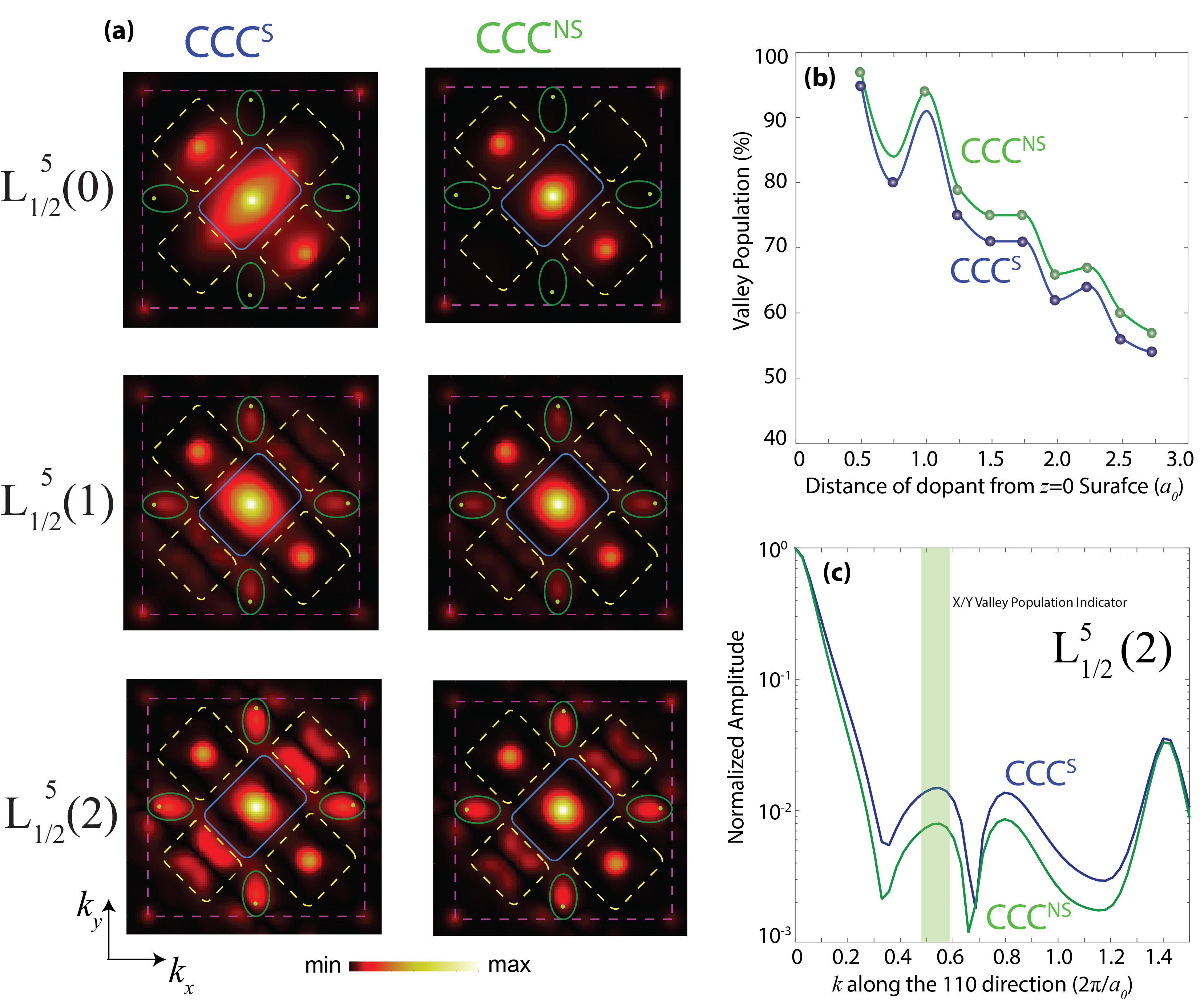
Next, we quantitatively compare the presence of bright features in the STM images with the actual spatial distribution of the donor wave functions. Here we define the spatial character of an STM image in the donor vicinity in terms of mean radius of its 1/100 contour – the contour of the normalised image where its peak intensity reduces to 1/100 value. Figures S4 (a) exhibit exemplary donor images computed from the two CCC models with donor position at L, along with the plots of (1/100)-contours. In figure S4 (b) we plot the extracted mean radii of the (1/100)-contours as a function of donor depths for both CCC implementations. To represent the dependence of tip-height on the calculations, we plot variation of the results due to a 5% variation in STM tip height around a fiducial value of 0.2 nm Usman et al. (2016), which indicates that tip height variation contribute only a small variation in the radii of the (1/100)-contours. To correlate this effect with the actual wave function charge densities, we also plot in supplementary figure S1(c) the mean radii of (1/100)-contours extracted from the corresponding wave function charge densities in the XY plane of the donor atom. The wave function contour radii for the CCCNS model are larger than for CCCS model, consistently following the trends of STM image contour radii for all of the top-most ten monolayers. This confirms that the extent of the computed STM images accurately represent the spatial distribution profile of the donor wave functions, which is directly modulated by the implementation of the underlying CCC model.
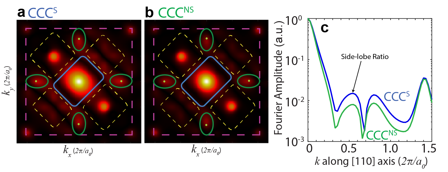
Whilst the real-space features of the STM images reflect the spatial variations of the donor wave functions, the difference in the spatial extent of the donor wave functions computed with the two CCC models results in a difference in their valley-configurations, which is easier to understand from the Fourier transform of the STM images Salfi et al. (2014). The ground state wave function for a bulk donor in silicon is comprised of equal contributions from the six degenerate valleys, however the proximity of the Z interface breaks this symmetry and lifts the degeneracy of valleys, thereby reducing (increasing) the energy (population) of Z-valley, compared to the X- and Y-valleys. The strength of this valley re-population effect is directly related to the interaction of donor wave function with the interface. In our discussion above, we have shown that the wave function charge density for the CCCNS model has larger amplitudes on silicon atoms compared to the CCCS model. Therefore we expect a correspondingly larger interaction of Z interface with the CCCNS state, resulting in a stronger valley re-population. To demonstrate this effect, in figure 5 (a) and (b) we plot the Fourier transform spectra of computed STM images from the two CCC models for a donor at L location. If the peak of Fourier spectrum at =0 is normalised to one, the second peak along the = line, defined as side-lobe ratio, has been shown to directly reflect the XY valley population of the corresponding donor state Salfi et al. (2014). We compare the side-lobe ratios in figure 5(c), which indicates a lower amplitude of the slide-lobe-ratio for CCCNS confirming a stronger valley re-population effect (see also supplementary section S3), consistent with the expected stronger interface effect. Therefore this work theoretically shows that the CCC induced differences in the valley configurations of the subsurface donor ground states are visible in the Fourier spectra of the corresponding STM images, providing a complementary way to further confirm the validity of the CCC implementation.
Motivation and challenges towards a future experiment:
In this work, we have focused on the effect of CCC on simulated STM images, evidencing differences in the spatial extent and valley population depending on the chosen CCC model. To be able to experimentally investigate CCC mechanism via STM imaging, the first step will require to develop a methodology to identify the donor depth. Depth identification of very shallow donors can be difficult due to the large Z-valley component but has been achieved for subsurface As donors Brazdova et al. (2017). Furthermore, the fabrication of dopants by atomically-precise fabrication technique Weber et al. (2012) is expected to provide a good estimate of the donor positions as recently shown for deeper P donor positions Usman et al. (2016). Although this study is based on the comparison between the computed P atom images, we note that the central-cell related differences are stronger between P and As donor wave functions, which is reflected in the corresponding STM images (see supplementary section S4). This could be exploited for the benchmarking of CCCs in the theoretical models. It is also noted that for a future theory-experiment comparison, additional effects such as electric field, strain, and quantum confinement will need to be taken into account, as these influence the STM images and their Fourier transform. Previous tight-binding study of bulk donors in silicon Usman et al. (2015b) has included the effects of electric field and strain, which could be extended for the simulation of STM images based on inputs from experimental setup.
Conclusions: In conclusion, this work has compared the computed STM images for two widely used implementations of the central-cell-correction models within the atomistic tight-binding framework and showed that the related effects on Si:P ground state wave functions are visible in both real-space features and frequency profiles of the simulated STM images for donor depths up to ten monolayers below the silicon surface. A quantitative correlation between the parameters such as spatial extent and valley-populations extracted from the computed STM images and the corresponding donor states is established. The theoretical demonstration of the visualisation of central-cell effects in the computed STM images lays the foundation for a future experiment to probe such effects, suggesting a possible route towards high-precision benchmarking of the central-cell-effects in theoretical models. Such a technique could play a vital role in the future studies of donor physics through atomic-scale understanding of the subsurface donor wave functions with higher accuracy compared to the existing empirical approaches.
Conflicts of interest: The authors declare no conflicts of interests.
Acknowledgements: This work is funded by the ARC Center of Excellence for Quantum Computation and Communication Technology (CE1100001027), and in part by the U.S. Army Research Office (W911NF-08-1-0527). Computational resources are acknowledged from NCN/Nanohub. This work was supported by computational resources provided by the Australian Government through Magnus Pawsey under the National Computational Merit Allocation Scheme.
Supplementary Material Section
S1. Atomistic Modelling of Donor Wave Functions
The atomistic simulations of electronic energies and states for a dopant in silicon are performed by solving an sp3d5s∗ tight-binding Hamiltonian. The sp3d5s∗ tight-binding parameters for the Si material are obtained from Boykin et al. Boykin et al. (2004), which have been optimised to accurately reproduce the Si bulk band structure. The phosphorous dopant atom is represented by a central-cell-correction (CCC) model. For this study, we have implemented two central-cell-correction models, namely CCCS and CCCNS. In the CCCS model, a Coulomb-like donor potential is screened by static dielectric constant () of silicon material and is given by:
| (1) |
where = 11.9 is the static dielectric constant of Si and is the charge on electron. The potential is cut-off to U()=U0 at the donor site, where the value of U0 is adjusted to match the experimentally measured binding energy spectra of 1s states Ahmed et al. (2009).
The second CCC model is much more extensive as it includes intrinsic strain and non-static dielectric screening effects Usman et al. (2015a). The donor atom is again represented by a Coulomb-like potential, which is cut-off to U()=U0 at the donor site, however it is screened by a -dependent dielectric function and is given by:
| (2) |
where A, , , and are fitting constant and have been numerically fitted as described in the literature Nara (1965). Additionally, the nearest-neighbor bond-lengths of Si:P are strained by 1.9% in accordance with the recent DFT study Overhof and Gerstmann (2004). The strain dependence is included in the tight-binding Hamiltonian by modifying the interatomic interaction energies in accordance with the Harrison’s scaling law Boykin et al. (2004), which has been previously verified against a number of experimental data sets Usman et al. (2011); Usman (2012); Usman et al. (2012); Ahmed et al. (2009).
The size of the simulation domain (Si box around the dopant) is chosen as 40 nm3, consisting of roughly 3 million atoms, with closed boundary conditions in all three spatial dimensions. The effect of Hydrogen passivation on the surface atoms is implemented in accordance with our published recipe Lee et al. (2004), which shifts the energies of the dangling bonds to avoid any spurious states in the energy range of interest. The multi-million-atom real-space Hamiltonian is solved by a parallel Lanczos algorithm to calculate the single-particle energies and wave functions of the dopant atom. The tight-binding Hamiltonian is implemented within the framework of NEMO-3D Klimeck et al. (2007b, a).
In the reported STM experiments Salfi et al. (2014), the (001) sample surface consists of dimer rows of Si atoms. We have incorporated this effect in our atomistic theory by implementing 21 surface reconstruction scheme, in which the surface silicon atoms are displaced in accordance with the published studies Craig and Smith (1990). The impact of the surface strain due to the 21 reconstruction is included in the tight-binding Hamiltonian by a generalization of the Harrison’s scaling law Boykin et al. (2004), where the inter-atomic interaction energies are modified with the strained bond length as , where is the unperturbed bond-length of Si lattice and is a scaling parameter whose magnitude depends on the type of the interaction being considered and is fitted to obtain hydrostatic deformation potentials.
The contact hyperfine interaction (A) is directly proportional to the charge density of the ground state wave function at the donor site , and the excited states do not contribute in the magnitude of A Usman et al. (2015b). The Z-valley population of the donor ground states is calculated by following the procedure described in the supplementary information of Salfi et al. Salfi et al. (2014). The size of the spatial distribution of the donor wave functions is defined in terms of its mean radius of in-plane (1/100)-contours – a contour where the amplitude of the normalised wave function decreases to 1/100 value. A direct comparison of these parameters computed from the two CCC models is presented in figure S1.
One important parameter of interest for exchange-based two qubit quantum logic gate design is the strength of exchange interaction (J) between two P donor atoms. Previous theoretical calculations have shown that the calculation of exchange interaction is very sensitive to the implementation of central-cell corrections Wellard and Hollenberg (2005); Pica et al. (2014b); Saraiva et al. (2014). We have computed the exchange interaction energies (J) for the two CCC models by using the Heitler-London formalism Wellard et al. (2003) as shown in figure S1 (d), and our calculations indicate a clear dependence of J on the implementation of CCC.
S2. Computation of STM Images
The calculation of the STM images is implemented by coupling the Bardeen’s tunnelling theory Bardeen (1961) and Chen’s derivative rule Chen (90 I) with our tight-binding wave function. In the tunnelling regime, the relationship between the applied bias (V) on the STM tip and the tunnelling current (I) is provided by the Bardeen’s formula:
| (3) |
where is the electronic charge, is the reduced Planck’s constant, is the Fermi distribution function, and is the tunnelling matrix element between the single electron states of the dopant (denoted by the subscript D) and of the STM tip (denoted by the subscript T). As derived by Chen in Ref. Chen, 90 I that the tunnelling matrix element, for all the cases related to STM measurements, can be reduced to a much simpler surface integral solved on a separation surface arbitrarily chosen at a point in-between the sample and STM tip. Therefore,
| (4) |
where is the single electron state of the sample (P or As dopant in Si), is the state of the single atom at the apex of the STM tip, and is an element on the separation surface .
In our calculation of the STM images, we follow Chen’s approach Chen (90 I), which reduces equation 4 to a very simple derivative rule where the tunnelling matrix element is simply proportional to a functional of the sample wave function computed at the tip location, (for assumed to be at the apex of the STM tip):
| (5) |
where the functional of the wave function, , is defined as a derivative (or the sum of derivatives) of the sample wave function – the direction and the dimensions of the derivatives depend on the orbital composition of the STM tip state. In our recent study Usman et al. (2016), we have shown that the tip orbital that dominates the STM tunnelling current is orbital, for which the equation 5 becomes:
| (6) |
The calculation of tunneling current is based on evaluating equation 6 at the the tip position. For this, we calculate the derivatives of the dopant wave function at the tip location, by computing its vacuum decay based on the Slater orbital real-space dependence Slater (1930), which satisfies the vacuum Schrödinger equation. Since the derivation of tight-binding Hamiltonian is independent of exact form of basis orbitals, the choice of basis orbitals is arbitrary. However the previous studies Lee et al. (2001); Nielsen et al. (2012) have shown that the use of Slater-type orbitals works well in the tight-binding theory as they accurately capture the atomic-scale screening of the materials. The analytical form of Slater-type orbitals for silicon material is given in Ref. Nielsen et al. (2012), which has been used in this work to describe real-space representation of the donor wave function.
It should be noted that the applied bias on STM tip was chosen to induce a small electric field, of the order of MV/m Salfi et al. (2014). The electric fields of such magnitudes are expected to negligibly perturb the real-space distribution and valley-population of the ground state of subsurface donors. Furthermore, when the STM tip bias was adjusted to introduce much larger electric field of the magnitude 10 MV/m, the valley population of the donor state was changed by less than 1% Salfi et al. (2017). Therefore in this work, we ignore the effect of electric field induced by the STM tip bias.
Finally, our low temperature STM data precludes the Si-tip model used to explain force-distance spectroscopies. This is not surprising because we work on chemically inert hydrogen terminated surfaces, at low temperature 4.2 K where chemical reactions will be highly suppressed.
S3. Fourier Domain Analysis of STM Images
Figure S3 plots the Fourier transform of the real-space images of P donor in L, L, and L locations, computed from both CCCS and CCCNS models. Since the real-space images computed from CCCNS model exhibit larger spatial extent (see Figure 2 in the main text), so the Fourier domain image exhibit lower amplitude in the frequency profile.
The ground state of a bulk P donor is comprised of equal contributions form six -space degenerate valleys. When the donor atom is brought closer to the Z=0 surface, it increases the Z-valley population and correspondingly X and Y valley populations decrease. The STM images directly probe the donor wave functions, therefore in the Fourier spectrum of the STM images, the -space valley information should be visible. As it turned out, that due to the strong inter-valley interference arising from the cross terms in and second derivatives involved due to dominant tunnelling from tip orbital, the components of the Fourier transform of STM images only provide information about the interference of X, Y, and Z valleys. From the previously published analysis Salfi et al. (2014), it has been shown that the frequency amplitudes in the so-called side-lobe ratios are qualitatively related to the corresponding X=Y valley populations of the donor wave functions. Figure S3 (b) plots the Z-valley populations directly extracted from the Fourier spectrum of the donor wave functions, as function of the donor depths, computed from both CCCS and CCCNS models. For both models, the Z-valley population increases as the donor atom becomes closer to the (001) surface. The larger increase in the Z-valley population for the CCCNS model is due to larger spatial extent of the corresponding wave function closer to the donor atom, which strongly interact with the interface as the donor atom is very close to the surface. To correlate this effect with the STM images, we also plot the = cut for L in figure S3 (c). The amplitude of the frequencies in the side-lobes is weaker for the CCCNS model compared to the CCCS model, which indicates low (high) population for XY (Z) valleys, consistent with the results of figure S3 (b). As the valley physics is a fundamental parameter of the donor wave functions directly modulated by the underlying CCC implementations, its direct availability in the Fourier spectrum of the STM images provides a viable path towards fine tuning of the CCC parameters directly based on STM measurements.
S4. Comparison of As and P STM Images
The ground state binding energies of the P and As donors are 45.5 meV and 53.7 meV as measured by the experiment Ramdas and Rodriguez (1981), therefore the As wave function is much more tightly bounded to the donor atom compared to the P wave function. This is captured in the central-cell-effects by having a larger value of the cut-off potential U0 for the As donor, which is 1.3 eV higher than for the P atom Usman et al. (2015b). As a result, the STM images for As donor are expected to be have small spatial size (and larger frequency components). Figure S4 compares the real space and Fourier space images of the As and P donors in panels (a) and (b), respectively. The donors are placed at the same atomic sites in L, L, and L. The difference between the STM images of As and P donors are quite evident, which indicates that STM imaging technique could differentiate between As and P donors. In fact, in future, if an experiment is performed by placing P and As atoms at the same lattice location, a direct comparison between the two measurements could provide a way to fine tune central-cell effects.
References
- Kane (1998) B. E. Kane, Nature 393, 133 (1998).
- Hollenberg et al. (2006) L. Hollenberg, A. D. Greentree, A. G. Fowler, and C. J. Wellard, Phys. Rev. B 74, 045311 (2006).
- Hill et al. (2015) C. Hill, E. Peretz, S. Hile, M. House, M. Fuechsle, S. Rogge, M. Y. Simmons, and L. Hollenberg, Science Advances 1, e1500707 (2015).
- Pica et al. (2016) G. Pica, B. W. Lovett, R. N. Bhatt, T. Schenkel, and S. A. Lyon, Phys. Rev. B 93, 035306 (2016).
- Fuechsle et al. (2012) M. Fuechsle, J. A. Miwa, S. Mahapatra, H. Ryu, S. Lee, O. Warschkow, L. C. L. Hollenberg, G. Klimeck, and M. Y. Simmons, Nature Nanotechnology 7, 242 (2012).
- Weber et al. (2012) B. Weber et al., Science 335, 64 (2012).
- Rahman et al. (2007) R. Rahman, C. J. Wellard, F. R. Bradbury, M. Prada, J. H. Cole, G. Klimeck, and L. C. L. Hollenberg, Phys. Rev. Lett. 99, 036403 (2007).
- Usman et al. (2015a) M. Usman, R. Rahman, J. Salfi, J. Bocquel, B. Voisin, S. Rogge, G. Klimeck, and L. C. L. Hollenberg, J. Phys.: Cond. Matt. 27, 154207 (2015a).
- Usman et al. (2015b) M. Usman, C. D. Hill, R. Rahman, G. Klimeck, M. Y. Simmons, S. Rogge, and L. C. L. Hollenberg, Phys. Rev. B 91, 245209 (2015b).
- Kalra et al. (2014) R. Kalra et al., Phys. Rev. X 4, 021044 (2014).
- Zwanenburg et al. (2013) F. Zwanenburg, A. S. Dzurak, A. Morello, M. Y. Simmons, L. C. L. Hollenberg, G. Klimeck, S. Rogge, S. N. Coppersmith, and M. A. Eriksson, Rev. Mod. Phys. 85, 961 (2013).
- Kohn and Luttinger (1955) W. Kohn and J. M. Luttinger, Phys. Rev. 98, 915 (1955).
- Wilson and Feher (1961) D. K. Wilson and G. Feher, Phys. Rev. 124, 1068 (1961).
- Pantelides and Sah (1974) S. T. Pantelides and C. T. Sah, Phys. Rev. B 10, 621 (1974).
- Martins et al. (2004) A. S. Martins, R. B. Capaz, and B. Koiller, Phys. Rev. B 69, 085320 (2004).
- Friesen (2005) M. Friesen, Phys. Rev. Lett. 94, 186403 (2005).
- Pica et al. (2014a) G. Pica, G. Wolfowicz, M. Urdampilleta, M. L. W. Thewalt, H. Riemann, N. V. Abrosimov, P. Becker, H.-J. Pohl, J. J. L. Morton, R. N. Bhatt, S. A. Lyon, and B. W. Lovett, Phys. Rev. B 90, 195204 (2014a).
- Gamble et al. (2015) J. Gamble et al., Phys. Rev. B 91, 235318 (2015).
- Wellard and Hollenberg (2005) C. J. Wellard and L. C. L. Hollenberg, Phys. Rev. B 72, 085202 (2005).
- Salfi et al. (2014) J. Salfi, J. A. Mol, R. Rahman, G. Klimeck, M. Y. Simmons, L. C. L. Hollenberg, and S. Rogge, Nature Materials 13, 605 (2014).
- Usman et al. (2016) M. Usman, J. Bocquel, J. Salfi, B. Voisin, A. Tankasala, R. Rahman, M. Y. Simmons, S. Rogge, and L. Hollenberg, Nature Nanotechnology 11, 763 (2016).
- Pica et al. (2014b) G. Pica et al., Phys. Rev. B 89, 235306 (2014b).
- Saraiva et al. (2015) A. L. Saraiva, A. Baena, M. J. Calderon, and B. Koiller, J. Phys.: Cond. Matt. 27, 154208 (2015).
- Overhof and Gerstmann (2004) H. Overhof and U. Gerstmann, Phys. Rev. Lett. 92, 087602 (2004).
- Smith et al. (2016) J. S. Smith, A. Budi, M. C. Per, N. Vogt, D. W. Drumm, L. C. L. Hollenberg, J. H. Cole, and S. P. Russo, arXiv:1612.00569 (2016).
- Koiller et al. (2002) B. Koiller, X. Hu, and S. D. Sarma, Phys. Rev. B 66, 115201 (2002).
- Ahmed et al. (2009) S. Ahmed, N. Kharche, R. Rahman, M. Usman, S. Lee, H. Ryu, H. Bae, S. Clark, B. Haley, M. Naumov, F. Saied, M. Korkusinski, R. Kennel, M. McLennan, T. B. Boykin, and G. Klimeck, “Multimillion atom simulations with nemo3d,” in Encyclopedia of Complexity and Systems Science, edited by R. A. Meyers (Springer New York, New York, NY, 2009) pp. 5745–5783.
- Nara (1965) H. Nara, J. Phys. Soc. Jap. 20, 778 (1965).
- Klimeck et al. (2007a) G. Klimeck, S. Ahmed, N. Kharche, M. Korkusinski, M. Usman, M. Parada, and T. Boykin, IEEE Trans. Elect. Dev. 54, 2090 (2007a).
- Boykin et al. (2004) T. B. Boykin, G. Klimeck, and F. Oyafuso, Phys. Rev. B 69, 115201 (2004).
- Ramdas and Rodriguez (1981) A. K. Ramdas and S. Rodriguez, Rep. Prog. Phys. 44, 1297 (1981).
- Salfi et al. (2017) J. Salfi et al., arXiv:1706.09261 (2017).
- Slater (1930) J. C. Slater, Phys. Rev. 36, 57 (1930).
- Bardeen (1961) J. Bardeen, Phys. Rev. Lett. 6, 57 (1961).
- Chen (90 I) C. J. Chen, Phys. Rev. B 42, 8841 (1990-I).
- Blanco et al. (2006) J. M. Blanco et al., Prog. Surf. Sci. 81, 403 (2006).
- Chaika et al. (2010) A. N. Chaika, S. S. Nazin, V. N. Semenov, S. I. Bozhko, O. Lubben, S. A. Krasnikov, K. Radican, and I. V. Shvets, Euro Phys. Lett. 92, 46003 (2010).
- Teobaldi et al. (2012) G. Teobaldi, E. Inami, J. Kanasaki, K. Tanimura, and A. L. Shluger, Phys. Rev. B 85, 085433 (2012).
- Feher (1959) G. Feher, Phys. Rev. 114, 1219 (1959).
- Brazdova et al. (2017) V. Brazdova, D. Bowler, K. Sinthiptharakoon, P. Studer, A. Rahnejat, N. Curson, S. Schofield, and A. Fisher, Phys. Rev. B 95, 075408 (2017).
- Usman et al. (2011) M. Usman et al., Phys. Rev. B 84, 115321 (2011).
- Usman (2012) M. Usman, Phys. Rev. B 86, 155444 (2012).
- Usman et al. (2012) M. Usman et al., Nanotechnology 23, 165202 (2012).
- Lee et al. (2004) S. Lee et al., Phys. Rev. B 69, 045316 (2004).
- Klimeck et al. (2007b) G. Klimeck, S. Ahmed, H. Bae, N. Kharche, S. Clark, B. Haley, S. Lee, M. Naumov, H. Ryu, F. Saied, M. .Prada, M. Korkusinski, T. B. Boykin, and R. Rahman, IEEE Trans. Elect. Dev. 54, 2079 (2007b).
- Craig and Smith (1990) B. I. Craig and P. V. Smith, Surface Science 226, L55 (1990).
- Saraiva et al. (2014) A. Saraiva et al., arXiv:1407.8224v1 (2014).
- Wellard et al. (2003) C. J. Wellard, L. C. L. Hollenberg, F. Parisoli, L. M. Kettle, H.-S. Goan, J. A. L. McIntosh, and D. N. Jamieson1, Phys. Rev. B 68, 195209 (2003).
- Lee et al. (2001) S. Lee et al., Phys. Rev. B 63, 195318 (2001).
- Nielsen et al. (2012) E. Nielsen, R. Rahman, and R. P. Muller, J. Appl. Phys. 112, 114304 (2012).