Photon-assisted Dynamical Coulomb Blockade in a Tunnel Junction
Abstract
We report measurements of photon-assisted transport and noise in a tunnel junction in the regime of dynamical Coulomb blockade. We have measured both dc non-linear transport and low frequency noise in the presence of an ac excitation at frequencies up to 33 GHz. In both experiments, at very low temperatures, we observe replicas at finite voltage of the zero bias features, a phenomenon characteristic of photon emission/absorption. However, the ac voltage necessary to explain our data is notably different for transport and noise, indicating that usual theory of photon-assisted phenomena fails to account for our observations.
Introduction. The physics of Dynamical Coulomb Blockade (DCB) in a tunnel junction - two metallic contacts separated by a thin insulating barrier - can be understood in simple terms: when an electron tunnels through the barrier, the charge on the contacts suddenly changes by an amount equal to . This results in a sudden change in the voltage across the junction given by with the capacitance between the contacts. Since the statistics of the electron tunneling across the barrier is driven by , it follows that next electrons have less probability to cross the barrierLevitov et al. (1996). When two tunnel junctions are in series, thus defining a conducting island between the two insulating barriers, a complete blocking of electron transport may occur at very low temperature , referred to as Coulomb blockade Devoret and Grabert (1992). With one junction only, the charge accumulated in the contacts leaks continuously into the rest of the circuit, leading to a progressive recovery of the possibility to have subsequent tunneling events Averin and Nazarov (1992). This phenomenon occurs on a time scale that depends on the circuit in which the junction is embedded, given for example by the product if the electromagnetic environment of the junction consists of a resistor . This mechanism gives its dynamical aspect to the DCB, which can be seen as a frequency-dependent feedback of the electromagnetic environment of the junction on electron transport. It is the same feedback that leads to corrections to high order cumulants of current fluctuations (in both cases current fluctuations generated by the environment also matter) Beenakker et al. (2003); Reulet et al. (2003); Reulet (2005).
The theory of DCB is well established Devoret et al. (1990); Ingold and Nazarov (1992) and has been successfully confirmed by many transport experiments Delsing et al. (1989); Geerligs et al. (1989); Cleland et al. (1992); Holst et al. (1994); Pierre et al. (2001). It consists of describing the electromagnetic environment of the junction by a collection of modes characterized by their density and population. In this picture, the environment authorizes inelastic tunneling of the electrons, which is possible only if the energy gained or lost by the electron can be accommodated by the environment. While very efficient, this description however seems to rely on different ingredients than the description of DCB by feedback. In particular, the dynamical response of the environment does not appear in a clear way.
Here we report an experiment that aims at probing the dynamical aspect of DCB by measuring the dc transport in a tunnel junction embedded in a resistive environment (the standard configuration for the observation of DCB) in the presence of an ac voltage. The frequency and amplitude of the excitation can be tuned to explore different regimes, from weak to strong , and from slow to fast excitation. Together with the dc nonlinear transport, we measure the zero frequency current noise to determine the ac voltage experienced by the junction, thus leaving no free parameter to fit the experimental transport data. We show that our transport data cannot be explained by recent theories that include the periodic voltage drive into the theory Safi and Sukhorukov (2010); Grabert (2015) if we use the values of the ac voltage given by the noise measurements.
Experimental Setup. Measurements are carried out on a 1 m 500 nm Al/Al oxide/Al tunnel junction fabricated by electrolitography using the Dolan bridge techniqueDolan (1977). The sample is placed in a dilution refrigerator of base temperature mK. A strong permanent magnet placed underneath the sample keeps the aluminum in its normal, non-superconducting state. The experimental setup is shown in Fig. 1. The junction is dc biased through a bias tee and ac biased through a 16 dB directional coupler placed between the bias tee and the junction. The dc biasing is performed through a 1 M resistor at room temperature and cryogenic low pass filters (not shown). Thus the sample of resistance (measured at high voltage), is effectively current biased at low frequency. We measure both the dc voltage across the junction and the differential resistance with usual lock-in technique. The sample’s current fluctuations are attenuated by a 6 dB cryogenic attenuator placed at the lowest temperature, amplified in the range 1 MHz-1 GHz by a cryogenic amplifier on the 3 K stage of the refrigerator, then further amplified at room temperature and bandpass filtered in the 1-80 MHz range. The power of the resulting signal is measured by a power detector as a function of the dc current as well as its derivative . The purpose of the attenuator is threefold. First it offers the junction a well defined resistive environment so that the electromagnetic environment of the junction is well described by its geometric capacitance in parallel with a resistor . Second, it attenuates the noise emitted by the amplifier towards the junction by a factor , thus keeping the electron temperature reasonably low (according to our noise measurements, mK, see below). Third, it attenuates the noise coming from the amplifier and reflected by the sample. At low frequency, the impedance of the sample is purely resistive, so the low frequency reflection coefficient is , with the differential resistance of the junction ( at high voltage). The detected power is related to the noise spectral density of the tunnel junction by:
| (1) |
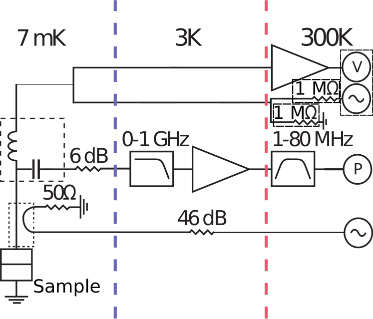
where is the noise temperature of the sample, the equivalent temperature of the noise emitted by the amplifier towards the sample, the equivalent temperature of the noise added by the setup and the power gain of the setup. Since depends on the bias, so does . Thus the bias dependence of comes from that of the noise generated by the sample as well as from the noise of the amplifier being reflected in a bias-dependent way. Since , the presence of the attenuator is essential. The amount of attenuation is chosen so as to keep enough signal while greatly attenuating the reflection of the amplifier’s noise. An ac excitation can be sent to the sample through the 2-40 GHz coupler placed next to it. The relevant frequency scale for the circuit is given by an inverse ”RC” time where ”R” corresponds to the parallel combination of and , i.e. . In order to know we have measured the frequency dependence of both the reflection coefficient of the bare junction and the noise emitted by the junction with high bias (data not shown). We observe GHz.
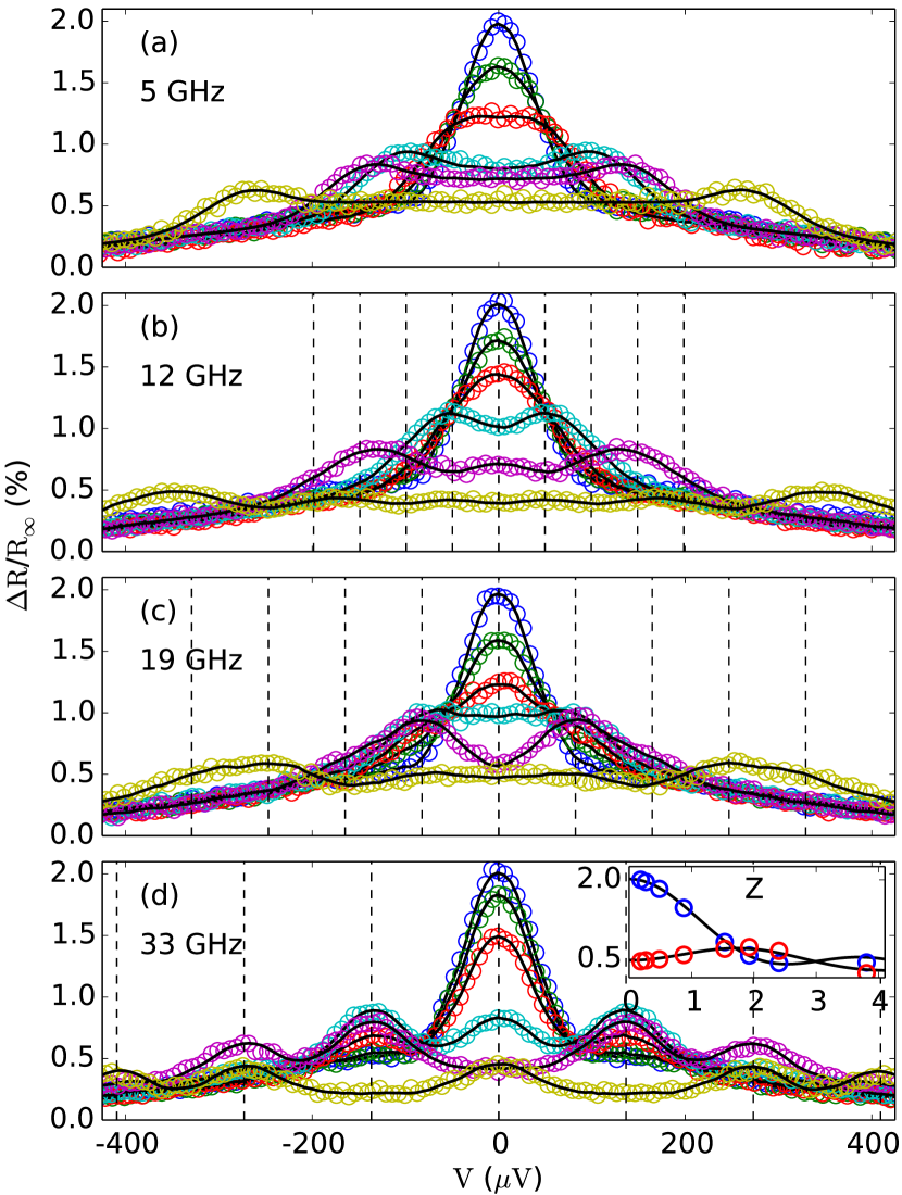
Results: differential resistance. We show in Fig. 2 the measurement of vs. at very low electron temperature ( mK), with the excess resistance. In the absence of ac excitation (dark blue curves in Fig. 2(a)-(d)) we observe a peak at zero bias, characteristic of DCB. This peak decreases when increases and disappears at K. In the presence of ac bias of frequency , we observe replicas of the central DCB peak that appear at finite voltage. Fig. 2 shows our results for excitations GHz (a), 12 GHz (b), 19.9 GHz (c) and 33 GHz (d). The positions of the replicas depend on the excitation frequency and are given by with integer (vertical dashed lines in Fig. 2). At low excitation frequency GHz, there is a strong overlap between the replicas. As the frequency increases, the peaks are more and more separated, and clearly distinguishable at GHz and GHz. We observe that the amplitude of the various peaks, including the one at zero voltage, depends in a non-trivial way on ac voltage, clearly indicating that our observations are not due to simple heating of the electrons by the ac excitation, see inset of Fig. 2(d).
Interpretation: Tien-Gordon mechanism. Similar observations have been performed a long time ago with Josephson junctions Tien and Gordon (1963). These observations are well understood if the only effect of the ac excitation is to induce a time-dependent, homogeneous voltage in one of the contacts. This voltage induces a time dependent phase in the electron wavefunctions in the contact given by . For a sinewave excitation , this phase results in the (current-voltage) and (noise-voltage) characteristics of the Josephson junction being modified into:
| (2) | ||||
with and the current and noise characteristics of the junction without ac excitation. Here are the Bessel functions of the first kind and . This formula predicts that the characteristics of the junction is a superposition of many copies of the original characteristic shifted in voltage by with weights given by . Clearly this result is not restricted to the characteristic of Josephson junctions but should apply to a broader range of quantities and devices. An important condition is however the absence of dynamical degrees of freedom in the system. Let us consider for example a mesoscopic diffusive wire. Since such a conductor is linear, its characteristics is not modified by the ac excitation, in agreement with Eq. (2), since . However, its shot noise does show replicas that are well described by Eq. (2) provided the excitation frequency is low when compared to the inverse diffusion time of the wire. Such replicas have been observed experimentally in the noise of wires Schoelkopf et al. (1998), tunnel junctions Gabelli and Reulet (2008) and quantum point contacts Zakka-Bajjani et al. (2007). The breakdown of Eq. (2) at high frequencies has been calculated Shytov (2005); Bagrets and Pistolesi (2007) but not yet observed. The condititions of validity of Eq. (2) can also be understood in the Landauer-Büttiker framework of quantum transport, where the transport properties of the sample are embedded in transmission coefficients. In this description, Eq. (2) is obtained only if the transmission coefficients are energy independent, as for a tunnel junction. However, DCB induces energy dependence in the transmissions even in a tunnel junction Matveev et al. (1993); Kindermann and Nazarov (2003), thus Eq. (2) might not hold. Furthermore, following Kindermann and Nazarov (2003), at low voltage and temperature, the strength of the energy dependence should be influenced by the environmental impedance at the excitation frequency , thus DCB might be different for or . Our experiment allows to probe the two regimes, where the charge has time to be evacuated before the ac voltage reverses or not. Recent theoretical papers have explicitly addressed the case of DCB in a tunnel junction in the presence of an ac voltage Safi and Sukhorukov (2010); Grabert (2015). Despite what we just discussed, the prediction is that Eq. (2) should be still valid. The only dynamical effect is that the ac voltage seen by the sample depends on frequency since the electromagnetic environment acts as a low-pass filter for the excitation. It is thus crucial to have a way to know the actual experienced by the sample, which is provided by the measurement of low frequency noise.
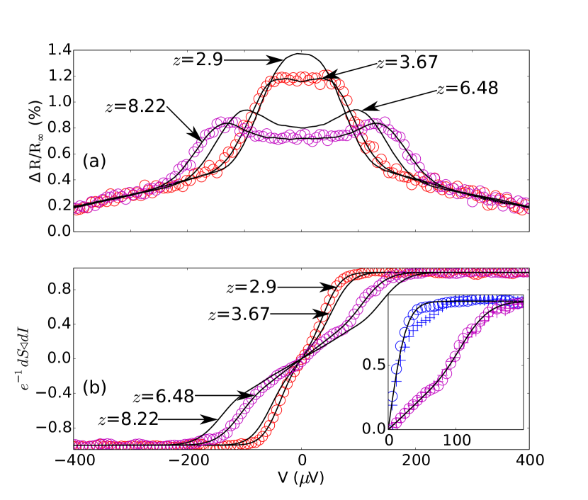
Results: noise. In order to probe potential dynamical effects in the photon-assisted DCB, it is necessary to calibrate the voltage experienced by the junction for each excitation frequency. We have done this by measuring the low frequency photon-assisted noise of the junction as in Gasse et al. (2013). We show in Fig. 3(b) results for the normalized differential noise , for an ac excitation at GHz. DCB corrections to the noise are of the order of a few % and can be neglected Altimiras et al. (2014), so we can fit our data with the usual theory Lesovik and Levitov (1994). However corrections due to the bias-dependent reflection of the noise of the amplifier must be taken into account, according to Eq. (1). The only unknown parameter is , the noise of the amplifier that is emitted towards the sample, which we determine as follows. The differential noise vs. in the absence of ac excitations should look like a step function, the width of which is inversely proportional to the temperature. As shown in the inset of Fig. 3(b), the experimental curves show additional steps. These steps are very well taken into account if we fit the data by Eq. (1) with K 111Similar extra steps have been reported in Altimiras et al. (2014) and attributed to the noise being measured given by non-symmetrized current-current correlator. This discussion is irrelevant here since our measurement corresponds to zero frequency noise, for which commutativity of current operators is not an issue.. This represents about half the total noise temperature of the amplifier, which is typical for such component. We show in Fig. 3(b) the normalized differential noise after correction. Corrected data are very well fitted by usual theory (Eq. (2)) with an electron temperature varying from mK at up to mK at the highest excitations (33 GHz, 3.8). This apparent heating of the electrons by the microwave excitation does not appear in the transport data: photon-assisted transport is very well fitted by considering replicas of the data taken at , i.e. at mK: peaks in are not broadened by the ac excitation. Taking replicas of transport measured at higher temperature yields to a much poorer fit. From the noise measurements we can infer the renormalized ac voltage across the junction for each excitation frequency. Note that the contribution of the reflected noise is most important when depends strongly on bias, i.e. mainly at low ac excitation: in the inset of Fig. 3(b) while the raw data at (blue crosses) clearly have an extra step as compared with the corrected data (blue circles), the effect of the correction becomes negligible at (purple crosses/circles).
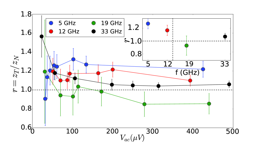
Interpretation: effective ac voltage. In order to compare experiment with theory we fit the transport data using Eq. (2) leaving the ac voltage as the only fitting parameter (solid lines on Fig. 2). For the characteristics in the absence of ac excitation, we take the experimental data at . The agreement between theory and data is excellent. Then we compare the rescaled values of the ac voltage used to fit the transport data with those extracted from our noise measurements : we show in Fig. 4 the ratio as a function the ac excitation obtained from noise measurements. While for low excitation the uncertainty on does not allow for a definitive conclusion, one clearly observes at high ac voltages. In particular, all values of are greater than unity for at all frequencies except GHz for which . An example of the discrepancy in between transport and noise is reported in Fig. 3 where differential resistance (a) and differential noise (b) are plotted vs. dc voltage for two excitation powers at GHz. While each of the curves can be very well fitted, it is clearly impossible to fit both transport and noise with the same . The ratio is plotted as a function of frequency in the inset of Fig. 4. The characteristic frequency GHz is indicated as a vertical dashed line. One should also have at low enough frequency.
A measurement of photo-assisted transport in the DCB regime has been reported in Parlavecchio et al. (2015). Unfortunately, only one frequency and one value of the ac voltage () have been measured, and there was no way to calibrate beside estimating the attenuation in the circuit. Thus the phenomenon we report here could not have been observed in Parlavecchio et al. (2015).
Conclusion. Our experiments show that Tien-Gordon mechanism applied to the usual theory of transport and noise of a tunnel junction in a resistive environment does not explain our observations, suggesting the existence of dynamical phenomena not well taken into account. For example, the ac voltage experienced by the sample should depend on the value of the ac complex impedance of the junction at the excitation frequency, which itself depends of the dc and ac bias of the sample Joyez et al. (1998); Parlavecchio et al. (2015); Altimiras et al. (2016). The ac excitation of the sample may also induce non-thermal distribution functions in the contacts that influence differently the noise and transport. 222Indeed, we note that our photon-assisted transport data are well fitted by taking replicas of the data at and the lowest temperature, whereas noise data at high excitation show an increased effective temperature.333Such effects have been discussed in similar samples where the amplitude of quantum oscillations could not be explained by the ac voltage excitation deduced from photon-assisted noise measurements Gasse et al. (2013). More experiments are called for, for example with a different electromagnetic environment, or using non-classical light as recently proposed Souquet et al. (2014), in order to probe more in depth the dynamical properties of DCB.
We acknowledge fruitful discussions with A. Clerk. We thank G. Laliberté for technical help. This work was supported by the Canada Excellence Research Chairs, Government of Canada, Natural Sciences and Engineering Research Council of Canada, Québec MEIE, Québec FRQNT via INTRIQ, Université de Sherbrooke via EPIQ, and Canada Foundation for Innovation.
References
- Levitov et al. (1996) L. S. Levitov, H. Lee, and G. B. Lesovik, Journal of Mathematical Physics 37, 4845–4866 (1996).
- Devoret and Grabert (1992) M. H. Devoret and H. Grabert, NATO ASI Series (1992).
- Averin and Nazarov (1992) D. V. Averin and Y. V. Nazarov, Phys. Rev. Lett. 69, 1993–1996 (1992).
- Beenakker et al. (2003) C. W. J. Beenakker, M. Kindermann, and Y. V. Nazarov, Phys. Rev. Lett. 90, 176802 (2003).
- Reulet et al. (2003) B. Reulet, J. Senzier, and D. E. Prober, Phys. Rev. Lett. 91, 196601 (2003).
- Reulet (2005) B. Reulet, Les Houches , 361–382 (2005).
- Devoret et al. (1990) M. H. Devoret, D. Esteve, H. Grabert, G.-L. Ingold, H. Pothier, and C. Urbina, Phys. Rev. Lett. 64, 1824–1827 (1990).
- Ingold and Nazarov (1992) G.-L. Ingold and Y. V. Nazarov, Single Charge Tunneling , Plenum Press, New York (1992).
- Delsing et al. (1989) P. Delsing, K. K. Likharev, L. S. Kuzmin, and T. Claeson, Phys. Rev. Lett. 63, 1180–1183 (1989).
- Geerligs et al. (1989) L. J. Geerligs, M. Peters, L. E. M. de Groot, A. Verbruggen, and J. E. Mooij, Phys. Rev. Lett. 63, 326 (1989).
- Cleland et al. (1992) A. N. Cleland, J. M. Schmidt, and J. Clarke, Phys. Rev. B 45, 2950 (1992).
- Holst et al. (1994) T. Holst, D. Esteve, C. Urbina, and M. H. Devoret, Phys. Rev. Lett. 73, 3455–3458 (1994).
- Pierre et al. (2001) F. Pierre, H. Pothier, P. Joyez, N. O. Birge, D. Esteve, and M. H. Devoret, Phys. Rev. Lett. 86, 1590–1593 (2001).
- Safi and Sukhorukov (2010) I. Safi and E. V. Sukhorukov, EuroPhys. Lett. 91 (2010).
- Grabert (2015) H. Grabert, Phys. Rev. B 92, 245433 (2015).
- Dolan (1977) G. J. Dolan, App. Phys. Lett. 31, 337–339 (1977).
- Tien and Gordon (1963) P. K. Tien and J. P. Gordon, Phys Rev. 129, 647–651 (1963).
- Schoelkopf et al. (1998) R. J. Schoelkopf, A. A. Kozhevnikov, D. E. Prober, and M. J. Rooks, Phys. Rev. Lett. 80, 2437–2440 (1998).
- Gabelli and Reulet (2008) J. Gabelli and B. Reulet, Phys. Rev. Lett. 100, 026601 (2008).
- Zakka-Bajjani et al. (2007) E. Zakka-Bajjani, J. Ségala, F. Portier, P. Roche, D. C. Glattli, A. Cavanna, and Y. Jin, Phys. Rev. Lett. 99, 236803 (2007).
- Shytov (2005) A. V. Shytov, Phys. Rev. B 71, 085301 (2005).
- Bagrets and Pistolesi (2007) D. Bagrets and F. Pistolesi, Phys. Rev. B 75, 165315 (2007).
- Matveev et al. (1993) K. A. Matveev, D. Yue, and L. I. Glazman, Phys. Rev. Lett. 71, 3351–3354 (1993).
- Kindermann and Nazarov (2003) M. Kindermann and Y. V. Nazarov, Phys. Rev. Lett. 91, 136802 (2003).
- Gasse et al. (2013) G. Gasse, L. Spietz, C. Lupien, and B. Reulet, Phys. Rev. B 88, 241402 (2013).
- Altimiras et al. (2014) C. Altimiras, O. Parlavecchio, P. Joyez, D. Vion, P. Roche, D. Esteve, and F. Portier, Phys. Rev. Lett. 112 (2014).
- Lesovik and Levitov (1994) G. B. Lesovik and L. S. Levitov, Phys. Rev. Lett. 72, 538 (1994).
- Note (1) Similar extra steps have been reported in Altimiras et al. (2014) and attributed to the noise being measured given by non-symmetrized current-current correlator. This discussion is irrelevant here since our measurement corresponds to zero frequency noise, for which commutativity of current operators is not an issue.
- Parlavecchio et al. (2015) O. Parlavecchio, C. Altimiras, J.-R. Souquet, P. Simon, I. Safi, P. Joyez, D. Vion, P. Roche, D. Esteve, and F. Portier, Phys. Rev. Lett. 114, 126801 (2015).
- Joyez et al. (1998) P. Joyez, D. Esteve, and M. H. Devoret, Phys. Rev. Lett. 80, 1956–1959 (1998).
- Altimiras et al. (2016) C. Altimiras, F. Portier, and P. Joyez, Phys. Rev. X 6, 031002 (2016).
- Note (2) Indeed, we note that our photon-assisted transport data are well fitted by taking replicas of the data at and the lowest temperature, whereas noise data at high excitation show an increased effective temperature.
- Note (3) Such effects have been discussed in similar samples where the amplitude of quantum oscillations could not be explained by the ac voltage excitation deduced from photon-assisted noise measurements Gasse et al. (2013).
- Souquet et al. (2014) J. R. Souquet, M. J. Woolley, J. Gabelli, P. Simon, and A. A. Clerk, Nat. Comm. 5, 5562 (2014).